Deconstruction of the Trap Model for the New Conducting State in 2D
In a series of recent papers, Altshuler, Maslov, and Pudalov[1] (AMP) proposed that the recent experimental finding by Kravchenko et al., Popović et al., Simmons et al., and Hanein et al.[2] of a new conducting state in a dilute 2D electron gas is really much ado about not very much. Namely, no new conducting state exists in a dilute 2D electron gas, and all experiments[3] observing a downturn in the resistivity will eventually observe an upturn at sufficiently low temperatures. In defense of this view, they offer[1] a trap model coupled with arguments from weak localization in which temperature-dependent traps are superimposed on a temperature-independent background potential. Within this model they predict that for a given concentration and strength of the trap potential, a downturn of the resistivity occurs but eventually the resistivity turns around and increases at some characteristic temperature, . They argue that should increase as the electron density increases. Consequently, saturation and eventual upturn of the resistivity should be easiest to observe in the high electron density samples. In fact, such an upturn has been observed, thus far, only in the highest density samples[4, 5], in apparent agreement with the prediction of the trap model. While general criticisms[6] have been levied at the AMP[1] model, which actually relies on four parameters to fit the experimental data, their calculation of has not been addressed. I show here that within the AMP model 1) in fact decreases with increasing electron density and 2) is on the order of , both of which are inconsistent with the experimental observations. Consequently, the lack of any upturn in the electrical resistivity in this temperature regime in the low electron density samples rules out the trapping model as a viable interpretation of the experiments on the new conducting state.
Within a model that has both temperature-dependent and temperature independent disorder, AMP write the resistivity accordingly as
| (1) |
In fact, a form of this type was first proposed by Pudalov for Si samples and later adopted in the context of the GaAs samples as a saturation of the resistivity was observed at low temperatures. Within the AMP model, the resistivity exhibits a minimum at
| (2) |
where and are numerical constants. In reaching the conclusion that increases with increasing electron density, AMP used the experimental fact that the denominator, , decreases as the carrier density increases.
It is unfortunate, however, that AMP did not consider the density dependence of , because to determine definitively the density dependence of a function, both the denominator and the numerator, rather than only the denominator, must be considered. The experiments clearly show that , the resistivity from the residual scattering, is strongly dependent on the carrier density, . For example, Hanein et al.[7] have shown that is inversely proportional to in GaAs heterostructures. Nearly exponential density dependence of was also reported for Si in Ref.[8] at . Inclusion of this effect leads to precisely the opposite conclusion regarding the density dependence of .
To show this, I analyse the beautiful data of Pudalov et al. of Ref. 3b on Si-MOSFET’s. Specifically, I focus on the data shown in the inset of Fig. 3. Shown there is a plot of the resistivity as a function of temperature for 11 electron densities. To consider the most favourable case for the AMP scenario, I determined the slope of the resistivity from its largest value. Because is inversely proportional to , my estimate will then be a lower bound to . Using the digitization feature of Ghostview, I simply chose two points on the steepest part of and then determined the slope. Consequently, my analysis does not fall prey to the ambiguity suggested in the response by AMP[9]. In addition, was obtained from the extrapolated leveled value of at zero tempearture. I display in Figure 1 a plot of versus the electron density obtained by analysing each of the eleven curves shown in the inset of Figure 3 in Ref. 3b. Further, to remove any ambiguity, I have provided the data points used in the analysis in the figure caption. As the figure clearly shows, predicted by the AMP model decreases (roughly as ), in contrast to their claim. Hence, rather than corroborating the AMP scenario, the upturn at high electron density now stands in stark contrast to what their model actually predicts.
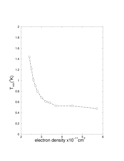
Further, the ’s determined here represent a lower bound to the turnaround temperature. As these temperatures are all on the order of 1K, they are certainly well accessible experimentally. However, no such turnaround has been observed in the experiments in the low density samples on the conducting side. In fact, the recent finding by Kravchenko and Klapwijk[10] that the resistivity in a low density Si sample does not exhibit an upturn down to 35 mK further points to the incorrectness of the AMP model.
We close by pointing out that [7]. Exponential decrease of the resistivity is an indication that some sort of charge gap exists in the single particle spectrum. Fermi liquids by definition cannot have a gap of any sort in the single particle spectrum. In fact, no traditional metal has a charge gap in the single particle spectrum. The only phase we know of that has a charge gap in the single particle spectrum that conducts at zero temperature is a superconductor. Hence, this would suggest that experiments sensitive to pair formation should be of utmost importance to the resolution of the nature of the charge carriers in the new conducting state in 2D.
REFERENCES
- [1] B. L. Altshuler, D. L. Maslov, and V. M. Pudalov, Phys. Stat. Sol. (b), 218, 193 (2000); B. L. Altshuler and D. L. Maslov, Phys. Rev. Lett. 82, 145 (1999).
- [2] S. V. Kravchenko et al., Phys. Rev. Lett. 77, 4938 (1996); D. Simonian, S. V. Kravchenko, M. P. Sarachik, and V. M. Pudalov, Phys. Rev. Lett. 79, 2304 (1997); D. Popović, A. B. Fowler, and S. Washburn, Phys. Rev. Lett. 79, 1543 (1997); M. Y. Simmons et al., Phys. Rev. Lett. 80, 1292 (1998); Y. Hanein et al., Phys. Rev. Lett. 80, 1288 (1998).
- [3] E. Abrahams, S. V. Kravchenko, and M. P. Sarachik, Rev. Mod. Phys. 73, 251 (2001).
- [4] a) V. M. Pudalov, G. Brunthaler, A. Prinz, and G. Bauer, JETP Lett. 68, 534 (1998); b) ibid, 70, 48 (1999).
- [5] A. R. Hamilton et al, Phys. Rev. Lett. 82, 1542 (1999).
- [6] S. V. Kravchenko, M. P. Sarachik, and D. Simonian, Phys. Rev. Lett. 83, 2091 (1999).
- [7] Y. Hanein et al., Phys. Rev. B 58, R7520 (1998).
- [8] V. M. Pudalov, G. Brunthaler, A. Prinz, and G. Bauer, JETP Lett. 68, 442 (1998).
- [9] B. L. Altshuler, G. W. Martin, D. L. Maslov, V. M. Pudalov, A. Prinz, G. Brunthaler, and G. Bauer, cond-mat/0008005.
- [10] S. V. Kravchenko and T. M. Klapwijk, Phys. Rev. Lett. 84, 2909 (2000).