Microscopic derivation of transport coefficients and boundary conditions in discrete drift-diffusion models of weakly coupled superlattices
Abstract
A discrete drift-diffusion model is derived from a microscopic sequential tunneling model of charge transport in weakly coupled superlattices provided temperatures are low or high enough. Realistic transport coefficients and novel contact current–field characteristic curves are calculated from microscopic expressions, knowing the design parameters of the superlattice. Boundary conditions clarify when possible self-sustained oscillations of the current are due to monopole or dipole recycling.
72.20.Ht, 73.50.Fq, 73.40.-c
I Introduction
At present, the theory of charge transport and pattern formation in
superlattices (SL) is in a fragmentary state. On the one hand, it is
possible to establish a quantum kinetic theory from first principles
by using Green function formalisms [1, 2]. However,
the resulting equations are hard to solve, even numerically, unless
a number of simplifications and assumptions are made [2, 3].
These include: (i) a constant electric field, (ii) simplified
scattering models, and (iii) a stationary current through the SL.
These assumptions directly exclude the description of electric field
domains and their dynamics although important results are still
obtained [3, 4]. The stationary current density probes the
difference between strongly and weakly coupled SL. It also indicates
when simpler theories yield good agreement with quantum kinetics.
The main simpler theories are (see Figure 1 of Ref. [3]):
(i) Semiclassical calculations of miniband transport using the
Boltzmann transport equation [5] or simplifications thereof, such
as hydrodynamic [6] or drift-diffusion [7] models. These
calculations hold for strongly coupled SL at low fields. In the miniband
transport regime, electrons traverse the whole SL miniband thereby
performing Bloch oscillations and giving rise to negative differential
conductivity (NDC) for large enough electric fields [8].
The latter may cause self-sustained oscillations of the current due to
recycling of charge dipole domains as in the Gunn effect of bulk n-GaAs
[9, 6].
(ii) Wannier-Stark (WS) hopping transport in which electrons move parallel to
the electric field through scattering processes including hopping transitions
between WS levels [10]. Calculations in this regime hold for
intermediate fields, larger than those corresponding to collisional
broadening of WS levels, but lower than those corresponding to resonant
tunneling.
(iii) Sequential tunneling calculations valid for weakly coupled SL
(coherence length smaller than one SL period) at basically any value
of the electric field [11, 12, 13]. A great advantage
of this formulation as compared with (i), (ii) or Green function
calculations is that boundary conditions can be derived naturally
and consistently from microscopic models [12].
On the other hand, the description of electric field domains and self-sustained oscillations in SL has been made by means of discrete drift models. These models use simplified forms of the tunneling current through SL barriers and discrete forms of the charge continuity and Poisson equations [14, 15, 16]. Although discrete drift models yield good descriptions of nonlinear phenomena in SL, bridging the gap between them and more microscopic descriptions [12, 13] is greatly desirable for further advancing both theory and experiments.
A step in this direction is attempted in the present paper. Our starting point is a microscopic description of a weakly coupled SL by means of discrete Poisson and charge continuity equations. In the latter the tunneling current through a barrier is a function of the electrochemical potentials of adjacent wells and the potential drops in them and in the barrier. This function is derived by means of the Transfer Hamiltonian method provided the intersubband scattering and the tunneling time are much smaller than the typical dielectric relaxation time [12]. From this microscopic model and for sufficiently low or high temperatures, we derive discrete drift-diffusion (DDD) equations for the field and charge at each SL period and appropriate boundary conditions. The drift velocity and diffusion coefficients in the DDD equations are nonlinear functions of the electric field which can be calculated from first principles for any weakly coupled SL. These equations are of great interest for the study of nonlinear dynamics in SL. They are simpler to study than microscopic model equations for which only numerical simulation results are available [18].
In the present work, natural boundary conditions for DDD equations are derived from microscopic calculations for the first time. Previous authors had to propose boundary conditions with adjustable parameters which gave qualitative agreement with experimental results [13, 14, 15, 16, 17]. The present boundary conditions relate current density and field at contacts and can be calculated for a given configuration of emitter and collector contact regions. As it is well-known, boundary conditions select the stable charge and field profiles in the SL, and therefore are crucial to understand which spatio-temporal structures will be observed in the SL for given values of the control parameters [13, 14, 15, 16, 17].
The rest of the paper is as follows. In Section II, we review the microscopic sequential resonant tunneling model. We obtain the minimal set of independent equations and boundary conditions describing this model. Our derivation of the DDD model is presented in Section III. Numerical evaluation of velocity, diffusion and contact coefficients for several SLs is presented in Section IV. Section V contains our conclusions. The Appendix contains an evaluation of the transport coefficients for negative values of the electric field.
II Microscopic sequential tunneling model
The main charge transport mechanism in a weakly coupled SL is sequential resonant tunneling. We shall assume that the macroscopic time scale of the self-sustained oscillations is larger than the tunneling time (defined as the time an electron needs to advance from one well to the next one). In turn, this latter time is supposed to be much larger than the intersubband scattering time. This means that we can assume the process of tunneling across a barrier to be stationary, with well-defined Fermi-Dirac distributions at each well, which depend on the instantaneous values of the electron density and potential drops. These densities and potentials vary only on the longer macroscopic time scale.
A Tunneling current
The tunneling current density across each barrier in the SL may be approximately calculated by means of the Transfer Hamiltonian method. We shall only quote the results here [12]. Let and be the currents in the emitter and collector contacts respectively, and let be the current through the th barrier which separates wells and . We have
| (1) | |||||
| (2) | |||||
| (3) | |||||
| (4) | |||||
| (5) | |||||
| (6) |
In these expressions:
-
, is the number of subbands in each well with energies (measured with respect to the common origin of potential drops: at the bottom of the emitter conduction band). are the Fermi energies of the emitter and collector regions calculated as functions of their doping density . and are the effective masses of the electrons at the wells and barriers, respectively.
-
are given by
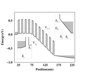
(7) (8) (9) (10) (11) where and are the wave vectors in the wells and the barriers, respectively. depends on the electric potential at the center of the th well, , whereas depends on the potential at the beginning of the th barrier, . See figure 1. and , , are the potential drops at the th barrier and well, respectively. We assume that the potential drops at barrier and wells are non-negative and that the electrons are singularly concentrated on a plane located at the end of each well (which is consistent with the choice of ; the choice of is dictated by the Transfer Hamiltonian method). The potential drops and correspond to the barriers separating the SL from the emitter and collector contacts, respectively. is the energy drop at the emitter region, and is the barrier height in the absence of potential drops.
-
is the dimensionless transmision probability through the th barrier separating wells and :
(12) provided .
-
and are the widths of wells and barriers respectively.
-
Scattering is included in our model by means of Lorentzian functions:
(13) (for the th well). The Lorentzian half-width is , where is the lifetime associated to any scattering process dominant in the sample (interface roughness, impurity scattering, phonon scattering…) [19, 20, 21, 22]. For the samples considered here, ranges from 1 to 10 meV[17]. Of course this phenomenological treatment of scattering could be improved by calculating microscopically the self-energy associated to one of the scattering proccesses mentioned above. However this restriction to one scattering mechanism would result in a loss of generality and simplicity of the model.
-
The integration variable takes on values from the bottom of the th well to infinity.
Of course this model can be improved by calculating microscopically the self-energies, which could include other scattering mechanisms (e.g. interface roughness, impurity effects [4, 13]) or even exchange-correlation effects (which affect the electron charge distribution in a self-consistent way). We have assumed that the electrons at each well are in local equilibrium with Fermi energies , which define the electron number densities :
| (14) |
Notice that the complicated dependence of the wave vectors and with the potential, , may be transferred to the Fermi energies by changing variables in the integrals of the system (4) so that the lower limit of integration (the bottom of the th well) is zero: . Then the resulting expressions have the same forms as Equations (4) and (14) if , , and in them are replaced by
| (15) | |||
| (16) |
respectively. is given by (11). The integrations now go from to infinity. Notice that is independent of the well index provided we assume that the energy level drops half the potential drop for the whole well with respect to its position in the absence of bias. Eq. (14) becomes
| (17) |
Here is obtained by substituting (the energy of the first subband measured from the bottom of a given well, therefore independent of electrostatics) instead of in (13). Notice that (17) defines a one-to-one relation between and which is independent of the index or the potential drops. The inverse function
gives the chemical potential or free energy per electron. This is the entropic part of the electrochemical potential (Fermi energy)
| (18) |
According to (18), the Fermi energy, (electrochemical potential), is the sum of the electrostatic energy at the th well, , and the chemical potential, .
After the change of variable in the integrals, the wave vectors in (4) become:
| (19) | |||
| (20) | |||
| (21) | |||
| (22) | |||
| (23) |
where now at the bottom of the th well. This shows that the tunneling current density, , in (4) is a function of: the temperature, and (therefore of and ), the potential drops , , , and :
| (24) |
Similarly, we have
| (25) | |||
| (26) |
B Balance and Poisson equations
The 2D electron densities evolve according to the following rate equations:
| (27) |
The voltage drops through the structure are calculated as follows. The Poisson equation yields the potential drops in the barriers, , and the wells, (see Fig. 1):
| (28) | |||||
| (29) |
where and are the GaAs and AlAs static permittivities respectively, is the 2D (areal) electron number density (to be determined) which is singularly concentrated on a plane located at the end of the th well, and is the 2D intentional doping at the wells.
C Boundary conditions
The emitter and collector layers can be described by the following equations:
| (30) | |||
| (31) | |||
| (32) |
To write the emitter equations (30), we assume that there are no charges in the emitter barrier [23]. Then the electric field across (see Fig. 1) is equal to that in the emitter barrier. Furthermore, the areal charge density required to create this electric field is provided by the emitter. is the density of states at the emitter Fermi energy . The collector equations (31) and (32) ensure that the electrons tunneling through the th (last) barrier are captured by the collector. They hold if the bias is large enough (see below). We assume that: (i) the region of length in the collector is completely depleted of electrons, (ii) there is local charge neutrality in the region of length between the end of the depletion layer and the collector, and (iii) the areal charge density required to create the local electric field is supplied by the collector. Notice that in (32) is the positive 2D charge density depleted in the collector region. Equations (31) and (32) hold provided , , and . For smaller biases resulting in , a boundary condition similar to (30) should be used instead of (31) and (32):
| (33) |
Notice that and have different meanings from and in (31).
The condition of overall voltage bias closes the set of equations:
| (34) |
This condition holds only if ; otherwise should be replaced by in (34).
Notice that we can find and as functions of from (30):
| (35) | |||
| (36) |
Similarly we can find by solving (31) and (32) in terms of and . From this equation and (31), we can find and as functions of :
| (37) | |||
| (38) | |||
| (39) |
where is the Heaviside unit step function. The boundary conditions (31) and (32) do not hold if . This occurs if . In this case, we should impose the alternative boundary conditions (33). From these, we obtain
| (40) | |||
| (41) |
The critical potential corresponds to . There is a small mismatch between (39) and (41) at this critical potential: , but . This imperfection can be fixed by using a more precise relation between the charge at the collector , and , but we choose not to delve more in these details. In all cases, we have shown that the potential drops at the barriers separating the SL from the contact regions uniquely determine the contact electrostatics.
D Elimination of the potential drops at the wells
The previous model has too many equations. We can eliminate the potential drops at the wells from the system. For (28) and (29) imply
| (43) |
Then the bias condition (34) becomes
| (44) | |||
| (45) |
where and . Instead of the rate equations (27), we can derive a form of Ampère’s law which explicitly contains the total current density . We differentiate (29) with respect to time and eliminate by using (27). The result is
| (46) |
where is the sum of displacement and tunneling currents. The time-dependent model consists of the equations (29), (45) and (46) [the currents are given by Eqs. (4), (14), (36), (39) and (43)], which contain the unknowns (), (), and . Thus we have a system of equations which, together with appropriate initial conditions, determine completely and self-consistently our problem. For convenience, let us list again the minimal set of equations we need to solve in order to determine completely all the unknowns:
| (47) | |||
| (48) | |||
| (49) | |||
| (50) | |||
| (51) | |||
| (52) | |||
| (53) |
Notice that the three last equations are constitutive relations obtained by substituting (43) in the functions , and of (24), (25) and (26), respectively. The functions and are given by (36) and (39), respectively. Equations (46) for may be considered the real boundary conditions for the barriers separating the SL from the contacts. These boundary conditions are the balance of current density including special tunneling current constitutive relations and . The latter depend on the electron densities at the extreme wells of the SL and the potential drops at the adjacent barriers.
III Derivation of the discrete drift-diffusion model
It is interesting to consider the relation (14) between the chemical potential and the electron density at a well for different temperature ranges:
| (54) |
Assuming that , we may approximate this expression by
| (55) |
Thus approaches a linear function of if . For the SL used in the experiments we have been referring to, is typically about 20 meV or 232 K. Thus “low temperature” can be “high enough temperature” in practice. Provided the Lorentzian is sufficiently narrow, , so that
| (56) |
Interestingly enough, a linear relation between and also holds at high temperatures. To derive it, notice that ln if and use this relation in (17):
| (57) |
If we now set , the result is
if , and . The additional condition (thermal energy small compared to the difference between the energies of the two lowest subbands) is needed to keep all electrons in the first subband. For otherwise the second subband may be populated and Equation (17) should be transformed accordingly. Thus our “high temperature” approximation can be satisfied in SL with large enough energy differences .
A different approximation is obtained if we first impose that :
| (58) |
This yields
| (59) |
and therefore
| (60) | |||
| (61) |
At low temperatures, the chemical potential again depends linearly on the electron density according to (56), whereas it has ideal gas logarithmic dependence at high temperatures.
The same considerations used to obtain (55) or (57) would indicate that the electron flux across the th barrier becomes
| (62) |
either at low or high enough temperatures. Here and are functions of , . They have dimensions of velocity and correspond to the forward and backward tunneling currents which were invoked in the derivation of phenomenological discrete drift models. When , or equivalently, , according to (4). Equation (17) implies that if , and therefore we conclude that at zero potential drops . Notice that becomes after changing variables in the integral (4). Then is approximately zero unless . For voltages larger than those in the first plateau of the current–voltage characteristic curve this condition does not hold. In fact for these voltages, the level of well is at a higher or equal potential than the level of well . Then .
The previous results yield DDD models with the potential drops at the barriers and the total current density as unknowns, the same as in Eqs. (46) - (53). The main difference with previously used discrete drift models is that the velocity depends on more than one potential drop. To obtain these simpler models, we further assume that and are approximately equal to an average field ( is an average permittivity to be chosen later). Then according to (43). This assumption departs from previous approximations and yields a new model. The point of contact with our previous results is that is the controlling factor in the expressions for and (the transmission coefficient contains an exponential factor, , which is almost constant at the energies contributing most to the integral). This controlling factor is uniquely determined by the potential drop
provided we define the average permittivity as
| (63) |
This expression corresponds to the equivalent capacitance of two capacitors in series. Thus the behavior of forward and backward drift velocities is most influenced by the potential drop and the new DDD model (see below) should yield results similar to those of the microscopic sequential tunneling model. We have
| (64) | |||
| (65) | |||
| (66) |
To calculate and from in (4), we replace , , and by , , and , respectively. The wavevectors in the integrand should be
| (67) | |||
| (68) | |||
| (69) | |||
| (70) | |||
| (71) |
and the integration variable ranges from 0 to . We substitute according to (17) in the result. Then we obtain a function :
| (72) |
[equivalent to setting , or after transforming this formula to the form (51)]. Notice that (as said above)
for the tunneling current to vanish at zero field and equal electron densities at adjacent wells. Furthermore, notice that vanishes if . Thus according to (56), vanishes if , which is certainly satisfied for all average fields larger than the first resonant field . In the low temperature limit (or in the high temperature limit mentioned earlier in this Section, provided it exists), we have
| (73) |
Then we may use
| (74) | |||||
| (75) |
to calculate the drift velocity and the diffusion coefficient from the tunneling current. The integrals from (4) appearing in these expressions may be approximated by means of the Laplace method: we should just expand their controlling factor mentioned before about its maximum value . The resulting formulas are cumbersome and we choose not to write them here. We show in the Appendix that , and .
Equations (73) to (75) may be used in (46) to write the Ampère law as
| (76) |
for . Poisson equation (48) becomes
| (77) |
for . Equations (76) and (77) constitute a DDD model which may be analyzed on its own together with appropriate bias and boundary conditions. As bias condition we adopt
| (78) |
Notice that potential drops at the contacts are represented only by the term . Equation (78) is obtained by inserting into (34), and omitting
for the sake of simplicity. For fields higher than the first resonance, , and (76) becomes
| (79) |
which is the usual discrete drift model used in previous theoretical studies [15, 16, 17].
In Section 2.1 of Ref. [13], A. Wacker derived a formula similar to (65) with and , for fields comparable to . At low fields, the resonant tunneling current between levels of adjacent fields was found to be proportional to and independent of . While the first approximation of Wacker’s (for fields close to higher resonances, , ) is compatible with our result (65), the second approximation is an artifact of the extra unnecessary assumption [13]. We shall show in Section IV that our drift velocity (74) may have at low fields the same shape as function for certain SL; see Fig. 2(a). Then the corresponding stationary current for a space homogeneous field profile with (which implies equality of chemical potentials at adjacent fields) will be proportional to and our result will agree with Wacker’s (for this special case). Fig. 2(b) shows that things may be different for a different SL configuration.
The boundary conditions for and are also Ampère’s law but now the tunneling currents (2) and (6) (from the emitter and to the collector, respectively) have to be used instead of (4). The same approximations as before yield
| (80) | |||||
| (81) | |||||
| (82) | |||||
| (83) |
Notice that there is no backward tunneling from the collector region to the SL because we are assuming that the potential drop is larger than . Assuming now that (81) and (83) are identities, we find
| (84) | |||||
| (85) | |||||
| (86) |
The tunneling current across a barrier is zero if the Fermi energies of the adjacent wells are equal. This occurs if the electron density at the first well takes on an appropriate value such that the corresponding Fermi energy equals that of the emitter. Then
and therefore
IV Numerical calculation of drift velocity and diffusion
In this Section, we shall calculate the functions , , , and for different SL used in experiments [17]. Fig. 2(a) depicts the electron drift velocity for the 9nm/4nm GaAs/AlAs SL (9/4 SL) of Ref. [17] calculated by means of (74) (at zero temperature; for simplilcity). The inset compares to the backward and forward velocities given by [ as in (75)] and . The rapidly decreasing diffusivity determines the position and height of the first peak in . Notice that behaves as expected from general considerations: it increases linearly for low electric fields, it reaches a maximum and then decays before the influence of the second resonance is felt. If decays faster, a rather different is found. Fig. 2(b) shows for the 13.3/2.7 SL: there is a wide region before the first peak in which .
Figures 3 and 4 show the boundary functions , and for the 9/4 and 13.3/2.7 SL, respectively. Again they behave as expected: (i) the emitter forward current peaks at the resonant values of the electric field [different from those of ], (ii) the emitter backward tunnel velocity decreases rapidly with field, and (iii) the collector forward velocity increases monotonically with field given the large difference between the Fermi energies of the last well and the collector.
The emitter forward current, , is compared in Figs. 5 and 6 to the drift current, , for different emitter doping values. Notice that the emitter current is systematically higher than the drift current for large emitter doping at positive electric fields. However, the total current density should remain between the first maximum and the minimum of the drift current. This means that the contact field should be negative, so that , with . Because of Poisson equation, (48), is larger than and, typically becomes positive. The electric field in the SL increases with distance from the emitter and a charge accumulation layer is formed (see Figure 5 of Ref. [12] for a similar stationary field profile corresponding to the full microscopic sequential tunneling model). Self-consistent current oscillations in this situation will be due to monopole recycling [18]. Notice that previous work on discrete drift models assumed a fixed excess of electrons in the first SL well as boundary condition [16, 17]. Again an emitter accumulation layer appeared and monopole self-oscillation resulted.
For smaller emitter doping, intersects on its second branch, and a charge depletion layer may be formed in the SL. Then there may be self-oscillations due to dipole recycling. These findings are fully consistent with the numerical results reported in Ref. [18] for the 13.3/2.7 SL. That paper reported coexistence and bistability of monopole and dipole self-oscillations for the first time. Coexistence and bistability were found for an intermediate emitter doping range (crossover range) lower than those used in experiments [18]. A different way to obtain dipole self-oscillations is to decrease the well width without changing contact doping. In this way, we have numerically checked that dipole self-oscillations are possible with emitter doping similar to those used in current experimental setups [17].
For the usual drift-diffusion model of the Gunn effect in bulk n-GaAs, the effect of boundary conditions on the self-oscillations of the current has been well-studied [24, 25]. In particular, asymptotic and numerical calculations for realistic metal-semiconductor contacts were performed some time ago [25]. Despite the different equations used in bulk semiconductors, these calculations provide results consistent with our present findings in SL: a boundary condition which yields accumulation (depletion) layer near injecting contact may yield current self-oscillations due to monopole (dipole) recycling [25, 24]. However these similarities between discrete (SL) and continuous (bulk) drift-diffusion models should not tempt us into reaching hasty conclusions: discrete and continuous drift-diffusion models may have rather different traveling wave solutions [26]. In fact, it has been shown that (depending on current and doping), the DDD model may have monopole wave solutions which travel in the same direction as the motion of electrons, in the opposite direction, or remain stationary. In the continuum limit (continuous drift-diffusion model), wavefronts travel always in the same direction as the electrons [26]. These features of the DDD equations may have experimentally observable consequences which will be explored elsewhere.
V Conclusions
Starting from a microscopic sequential tunneling model of transport in weakly coupled SL, a DDD model is derived in the limits of low or high temperature. Realistic transport coefficients and novel contact current–field characteristic curves are calculated from microscopic expressions, knowing the design parameters of the superlattice. Boundary conditions select stable spatio-temporal charge or field profiles in the SL. In prticular, they clarify when possible self-sustained oscillations of the current are due to monopole or dipole recycling.
ACKNOWLEDGMENTS
One of us (LLB) thanks Dr. Andreas Wacker for fruitful discussions and collaboration on discrete drift-diffusion models. We thank Dr. Ramón Aguado and Dr. Miguel Moscoso for fruitful discussions. This work was supported by the Spanish DGES through grants PB98-0142-C04-01 and PB96-0875, by the European Union TMR contracts ERB FMBX-CT97-0157 and FMRX-CT98-0180 and by the Community of Madrid, project 07N/0026/1998.
A Models for negative bias
When a negative voltage is applied, we should make sure that our formulas transform appropriately. For negative bias, the charge will be singularly concentrated on planes located at the beginning of the wells. Then we should write
| (A1) |
instead of (10) in the expressions (4). The change of variable (i.e., corresponds to zero energy at the bottom of well ) in the integral (4), then changes the wavevectors to
| (A2) | |||
| (A3) | |||
| (A4) | |||
| (A5) | |||
| (A6) |
instead of (23).
Given the new location of the singular charge planes (at the beginning of wells), (28) still holds, but (29) should be replaced by
| (A7) |
Then we find
| (A8) |
instead of (43). Inserting this equation in the functions (tunneling current under negative bias), we obtain new functions , instead of valid for positive voltage. To obtain a reduced model, we now set
| (A9) | |||
| (A10) | |||
| (A11) | |||
| (A12) | |||
| (A13) | |||
| (A14) | |||
| (A15) | |||
| (A16) | |||
| (A17) |
in the integrals (4) and let the variable of integration range from 0 to . This is equivalent to setting , and equal to in . Equations (4), (71), (A17) and the previous definitions in this Appendix imply
| (A18) | |||
| (A19) |
The Poisson equation (A7) still yields (77). Notice that the symmetry (A19) implies
| (A20) |
Given the difference between the states at the contact regions and the wells, the previous arguments cannot be used to extend the contact current–field characteristic curves to negative fields. Direct calculation of (84) - (86) by means of (2) and (6) yields the results depicted in Figures 3 and 4.
REFERENCES
- [1] L. P. Kadanoff and G. Baym, Quantum Statistical Mechanics. (Benjamin, New York, 1962); L. V. Keldysh, Sov. Phys. JETP 20, 1018 (1965) [Zh. Eksp. Theor. Fiz 47, 1515 (1964)].
- [2] H. Haug and A.-P. Jauho, Quantum Kinetics in Transport and Optics of Semiconductors (Springer, Berlin 1996).
- [3] A. Wacker and A.-P. Jauho, Phys. Rev. Lett. 80, 369 (1998).
- [4] A. Wacker, A.-P. Jauho S. Rott, A. Markus, P. Binder and G.H. Döhler, Phys. Rev. Lett. 83, 836 (1999).
- [5] J. F. Palmier, G. Etemadi, A. Sibille, M. Hadjazi, F. Mollot and R. Planel, Surface Sci. 267, 574 (1992); R.R. Gerhardts, Phys. Rev. B 48, 9178 (1993); A.A. Ignatov, E.P. Dodin and V.I. Shashkin, Mod. Phys. Lett. B 5, 1087 (1991).
- [6] M. Büttiker and H. Thomas, Phys. Rev. Lett. 38, 78 (1977); Z. Phys. B 34, 301 (1979); X.L. Lei, N.J.M. Horing and H.L. Cui, Phys. Rev. Lett. 66, 3277 (1991); J.C. Cao and X.L. Lei, Phys. Rev. B 60, 1871 (1999).
- [7] A. Sibille, J. F. Palmier, F. Mollot, H. Wang and J. C. Esnault, Phys. Rev. B 39, 6272 (1989).
- [8] L. Esaki and R. Tsu, IBM J. Res. Dev. 14, 61 (1970).
- [9] J. B. Gunn, Solid State Commun. 1, 88 (1963).
- [10] R. Tsu and G.H. Döhler, Phys. Rev. B 12, 680 (1975); S. Rott, N. Linder and G.H. Döhler, Superlatt. and Microstr. 21, 569 (1997); S. Rott, P. Binder, N. Linder and G.H. Döhler, Phys. Rev. B 59, 7334 (1999).
- [11] R.F. Kazarinov and R.A. Suris, Fiz. Tekh. Poluprov. 6, 148 (1972) [Sov. Phys. Semicond. 6, 120 (1972)].
- [12] R. Aguado, G. Platero, M. Moscoso and L.L. Bonilla, Phys. Rev. B 55, R16053 (1997).
- [13] A. Wacker, in Theory and transport properties of semiconductor nanostructures, edited by E. Schöll. Chapter 10. Chapman and Hill, New York, 1998.
- [14] F. Prengel, A. Wacker and E. Schöll, Phys. Rev. B 50, 1705 (1994).
- [15] L.L. Bonilla, J. Galán, J.A. Cuesta, F.C. Martínez and J. M. Molera, Phys. Rev. B 50, 8644 (1994).
- [16] L.L. Bonilla, in Nonlinear Dynamics and Pattern Formation in Semiconductors and Devices, edited by F.-J. Niedernostheide. Pages 1-20. Springer, Berlin, 1995; A. Wacker, M. Moscoso, M. Kindelan and L.L. Bonilla, Phys. Rev. B 55, 2466 (1997); L.L. Bonilla, M. Kindelan, M. Moscoso, and S. Venakides, SIAM J. Appl. Math. 57, 1588 (1997).
- [17] J. Kastrup, H.T. Grahn, R. Hey, K. Ploog, L.L. Bonilla, M. Kindelan, M. Moscoso, A. Wacker and J. Galán, Phys. Rev. B 55, 2476 (1997); J.W. Kantelhardt, H. T. Grahn, K. H. Ploog, M. Moscoso, A. Perales and L.L. Bonilla, Physica Status Solidi B 204, 500 (1997).
- [18] D. Sánchez, M. Moscoso, L. L. Bonilla, G. Platero and R. Aguado, Phys. Rev. B 60, 4489 (1999).
- [19] T. Weil and B. Vinter, Appl. Phys. Lett. 50, 1281 (1987).
- [20] R. Aguado and G. Platero, Phys. Rev. B 55, 12860 (1997).
- [21] R. Aguado and G. Platero, Superlattices and Microstructures, 22, 9 (1997).
- [22] G. Platero and R. Aguado, Appl. Phys. Lett. 70, 3546 (1997).
- [23] V. J. Goldman, D. C. Tsui and J. E. Cunningham, Phys. Rev. Lett. 58, 1256 (1987); Phys. Rev. B 35, 9387 (1987); J. Iñarrea and G. Platero, Europhys. Lett. 33, 477 (1996).
- [24] M. P. Shaw, H. L. Grubin and P. R. Solomon, The Gunn-Hilsum effect (Academic P., New York, 1979).
- [25] G. Gomila, J. M. Rubí, I. R. Cantalapiedra and L. L. Bonilla, Phys. Rev. E 56, 1490 (1997); L. L. Bonilla, I. R. Cantalapiedra, G. Gomila and J. M. Rubí, Phys. Rev. E 56, 1500 (1997).
- [26] A. Carpio, L. L. Bonilla, A. Wacker and E. Schöll, Phys. Rev. E, to appear.