TUNNELING MEASUREMENTS OF THE COULOMB PSEUDOGAP IN A TWO-DIMENSIONAL ELECTRON SYSTEM IN A QUANTIZING MAGNETIC FIELD
Abstract
We study the Coulomb pseudogap for tunneling into the two-dimensional electron system of high-mobility (Al,Ga)As/GaAs heterojunctions subjected to a quantizing magnetic field at filling factor . Tunnel current-voltage characteristics show that for the double maximum observed in the tunnel resistance at the pseudogap is linear in energy with a slope that depends on filling factor, magnetic field, and temperature. We give a qualitative account of the filling factor dependence of the pseudogap slope and we confirm the recently reported appearance of another relaxation time for tunneling at . For the tunnel resistance peaks at and 2/3 a completely different behaviour of the current-voltage curves is found and interpreted as manifestation of the fractional gap.
pacs:
PACS numbers: 72.20 My, 73.40 KpI Introduction
The integer quantized Hall effect in a two-dimensional (2D) system is understood to be a single particle effect. On the other hand it is now well known that the charge injection by tunneling into the 2D system at quantizing magnetic fields is very sensitive to many particle effects. Two kinds of tunneling experiments are possible: tunneling into the edge (so-called lateral tunneling, e.g., [1, 2, 3]) and into the bulk (or vertical tunneling [4, 5, 6, 7, 8, 9, 10]) of the 2D system. It is the vertical tunneling experiments that are a powerful tool for investigating the electron spectrum of 2D systems. In a pioneering paper [4] it was shown that the tunneling between a 2D electron gas and a 3D metallic layer reveals both gaps in the energy spectrum at integer or fractional filling factors originating from magnetic field quantization and a Coulomb pseudogap that is pinned to the Fermi level of the 2D system. The former correspond to cusps in the dependence of the 2D system energy on electron density and can be directly measured using alternative methods with or without vertical tunneling [11, 12] while the latter is seen directly only in vertical tunneling measurements [5, 6, 7, 8, 9, 10]. In the work of Ref. [5] the pseudogap was found to persist in a wide range of magnetic fields, depending weakly on filling factor. Alternative studies of tunneling between two high-mobility 2D electron systems pointed to the existence of a pseudogap with exponentially small tunnel density of states in the extreme magnetic quantum limit [6]. As long as the experiments of Refs. [4, 5] and Ref. [6] were performed on samples of very different quality and in the low or high magnetic field limit, respectively, it was unclear whether the gap observed by both experimental groups had the same physical origin. Recently it has been suggested that in all the above mentioned experiments the same pseudogap was investigated because all of the obtained results can be reproduced on one sample [7]; particularly, at the tunnel density of states in the pseudogap of Ref. [7] increases linearly at small and far more rapidly at larger distances from the Fermi energy. Quite an unexpected and peculiar result was reported in Ref. [8] that at filling factor the width of the pseudogap for tunneling between two equivalent 2D electron layers such as in Ref. [6] is roughly proportional to magnetic field.
A drastic increase of the pseudogap in the vicinity of filling factor manifested by a camel-back structure of the tunnel resistance was observed for tunneling from a 3D electron system into a high-mobility 2D electron gas [9]. This observation has been confirmed recently by time-resolved tunneling experiments of Ref. [10] where a corresponding camel-back structure was found in the relaxation time of the tunnel current at filling factors close to . In that work, however, attention has been paid to the observation of two strikingly different relaxation times, whereas the camel-back shape is not discussed. Measurements of current-voltage characteristics at showed that the pseudogap is roughly linear in energy near the Fermi level [9].
Theoretical models have been developed for the tunneling density of states in a 2D system in both the metallic and the insulating phase. In the absence of magnetic field, in a 2D metal with weak random potential the electron-electron interaction is believed to lead to a logarithmic correction that reduces the single-particle density of states at the Fermi energy [13] whereas in a 2D insulator with strongly localized electrons the tunnel density of states vanishes at the Fermi level linearly with energy , where is the dielectric permeability and is the electron charge [14]. The problem of vertical tunneling at zero temperature in quantizing magnetic fields has been tackled in many recent publications. For the metallic state these predict a Coulomb pseudogap with exponentially small density of states near [15, 16, 17, 18]. A similar result was obtained for the Wigner crystal insulating state [19] and the insulating state of weakly disordered 2D systems at high filling factors [20]. According to Refs. [15, 16, 19], the pseudogap should scale with the average interelectron distance. Finally, for the insulating phase with strong disorder the Coulomb-interaction-induced pseudogap is expected to be linear in energy with a background density of states at the Fermi energy [21]
| (1) |
where the factor is a bit different from the constant predicted in Ref. [14]. The linear dependence (1) survives even in the presence of a screening metallic electrode at distances from the 2D system comparable to the average interelectron distance [22].
The above theories give a qualitative account of all experimental results on the Coulomb pseudogap except as follows: (i) the absence of scaling of the pseudogap with average interelectron distance [8]; (ii) the drop of the coefficient with magnetic field [7]; and (iii) the pseudogap behaviour near filling factor [9, 10].
Here, we study in detail the 3D – 2D tunneling for high-quality 2D electron systems in quantizing magnetic fields at . Except for the tunnel resistance peaks at and 2/3, current-voltage () characteristics correspond to a pseudogap that is linear in energy. For the vicinity of , where the tunnel resistance exhibits a double maximum, we analyze the behaviour of the pseudogap with changing filling factor, magnetic field, and temperature. Furthermore, we present evidence of the existence of another relaxation time for tunneling. At filling factor and 2/3 very distinctive characteristics are observed that are likely to reflect the fractional gap.
II Samples and experimental technique
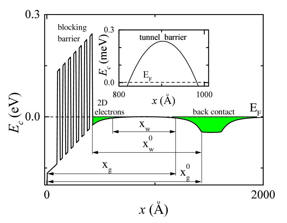
Our samples are metal-insulator-semiconductor (Al, Ga)As/GaAs heterojunctions with high mobility that contain, apart from a metallic gate on the front surface, a highly doped ( cm-3 Si) layer with thickness 20 nm in the bulk of GaAs. This layer remains well-conducting even at very low temperatures and serves as a back electrode. The four samples are prepared from two wafers grown on different MBE machines. The epitaxially grown layer sequence of the samples and the calculated behaviour of the conduction band bottom are shown in Fig. 1. A blocking barrier between the gate and the 2D electrons is formed by a short-period GaAs/AlAs superlattice capped by a thin GaAs layer. A wide but shallow tunnel barrier between the back electrode and the 2D electron system is created by the weak residual p-doping of the GaAs layer. The density of the 2D electrons is controlled by the gate voltage applied between the back electrode and the front gate, because electron transfer across the tunnel barrier brings the electron gas in the back electrode and the 2D electron system into equilibrium. The front gate and the heterojunction barrier are separated from the back electrode by the distances nm, nm in wafer A and nm, nm in wafer B. The gate area is equal to m2 for sample A1, 800 m2 for samples A2 and A3, and 3300 m2 for sample B.
The gate voltage is modulated with a small ac voltage so that an ac current is excited through the device. From the real and imaginary components of the current we derive information on both the thermodynamic density of states and tunnel resistance between the 2D electron system and back electrode. For the case of linear current-voltage dependences one obtains [5, 9]
| (2) |
where is the ac voltage frequency, and are the low and high frequency limits of the device capacitance, and the relaxation time is equal to
| (3) | |||||
| (4) |
where () is the tunnel resistance (resistivity), is the attempt frequency, is the single-particle density of states, and the distances replace , taking into account actual electron density distributions in the direction (Fig. 1). In the low frequency limit, the capacitance reflects the thermodynamic density of states [23], and the real current component is proportional to . In this limit, nonlinear tunnel characteristics are extracted from the measured and using the relations for the voltage and current across the tunnel barrier
| (5) |
We note that is defined as the difference of the electrochemical potentials across the tunnel barrier.
The measurements are performed using a standard lock-in technique in the frequency interval between 3 Hz and 2 kHz at temperatures between 30 and 880 mK and magnetic fields up to 16 T. The amplitude of the ac voltage across the sample is in the range 0.2 – 8 mV. In the analysis of nonlinear characteristics we take into account that it is the first Fourier harmonic of the ac current which is measured experimentally.
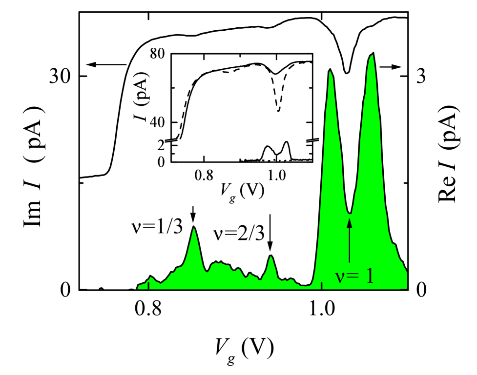
A typical experimental trace in the low frequency limit is presented in Fig. 2. The imaginary current component reflects the thermodynamic density of states with minima at integer and fractional fillings and is used to extract the gate voltage dependence of the electron density [12, 23]. This point is of importance because lateral transport experiments are principally impossible in a 2D system that is shunted by a 3D back electrode through a tunnel barrier. The real current component displays a background signal weakly dependent on filling factor, which was studied previously in Refs. [4, 5, 6, 7, 8], alongside with a camel-back structure at [9, 10] as well as peaks at and 2/3. In principle, such additional structures may be caused by a possible admixture of lateral transport: the small dissipative conductivity at integer fillings does not allow tunneling measurements between two identical 2D electron sheets [6, 8]. If the 2D electron system is charged from the 3D back electrode, there are no restrictions to the filling factors at which the tunneling experiments can be performed provided the 2D system and the tunnel barrier are homogeneous. In the case of an inhomogeneous tunnel barrier the in-plane transport may contribute significantly to measured values. We argue that the maxima observed here in the real component of the current close to do not reflect lateral transport effects in the 2D system: firstly, at the same temperature for filling factor no peaks are observed in the real current component although the dissipative conductivity is expected to be smaller than the one at (inset to Fig. 2); secondly, the behaviour discussed below, in particular, the frequency, temperature, and magnetic field dependences of the active current component as well as the behaviour of curves are inconsistent with the assumption of in-plane transport; thirdly, very similar data at have been obtained on samples with a different design of the tunnel barrier [10].
Because on one hand, the dissipative conductivity at fractional minima is expected to be higher than at and, on the other hand, the amplitudes of the observed peaks at and 2/3 are comparable to the value of at (Fig. 2), we conclude that the peaks observed at fractional filling factors are not due to lateral transport either.
III Experimental results
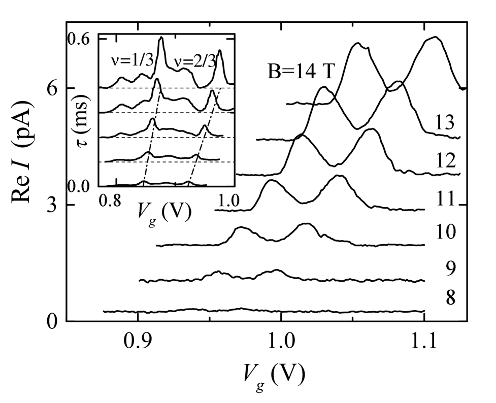
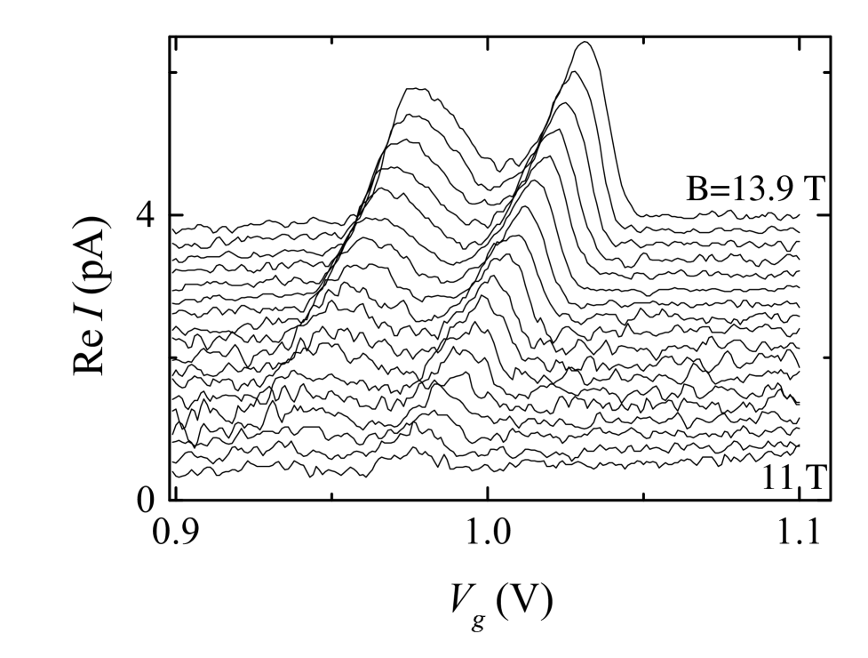
The genesis of the camel-back structure centered at with magnetic field is shown in Figs. 3 and 4 for the samples of both wafers. This structure emerges at a lower magnetic field for the higher quality 2D electron system of wafer A as indicated by the presence (absence) of tunnel resistance peaks at fractions and 2/3 for wafer A (B). As seen from the figures, the structure has a double-peak shape over the entire range of magnetic fields.
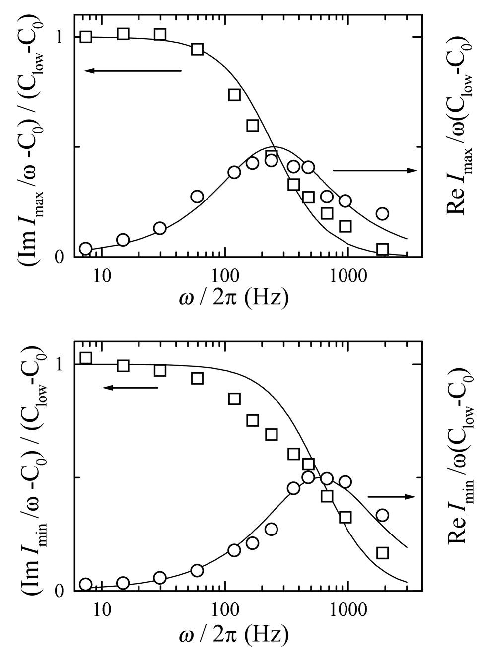
The frequency dependences of both current components measured at a maximum and at the minimum of the tunnel resistance at are presented in Fig. 5. Since at fixed modulation voltage the tunnel current would rise with frequency, we reduce to keep fixed and thus avoid possible influence of nonlinearities in this measurement. The formula (2) fits well the data points if the capacitance in Eq. (2) is replaced by a fitting parameter . This implies the presence of at least two tunneling channels with strongly different relaxation times: the parameter is a weight of the tunneling channel with the highest tunnel resistivity (and ) so that describes an ”effective area” in the sample, which can be expected to be cluster-like as inferred from the absence of lateral transport. The corresponding maximum of the real current component as a function of frequency is proportional to . In the low frequency limit discussed below, the tunnel current through the so-introduced effective area is also proportional to , i.e., one should replace in Eq. (5) by , whereas the expressions (4,5) for and remain valid since both of these values are related to the effective area. The fit in Fig. 5 yields and for the maximum and minimum of the tunnel resistance, respectively. We find that these values do not significantly change with magnetic field. Furthermore, on all samples the value exhibits a minimum at that is similar to the minimum in (Fig. 2). We emphasize that the characteristic double-peak shape persists in (or ): after dividing the double peak in by for extracting the tunnel resistance there remains still a minimum at with % depth.
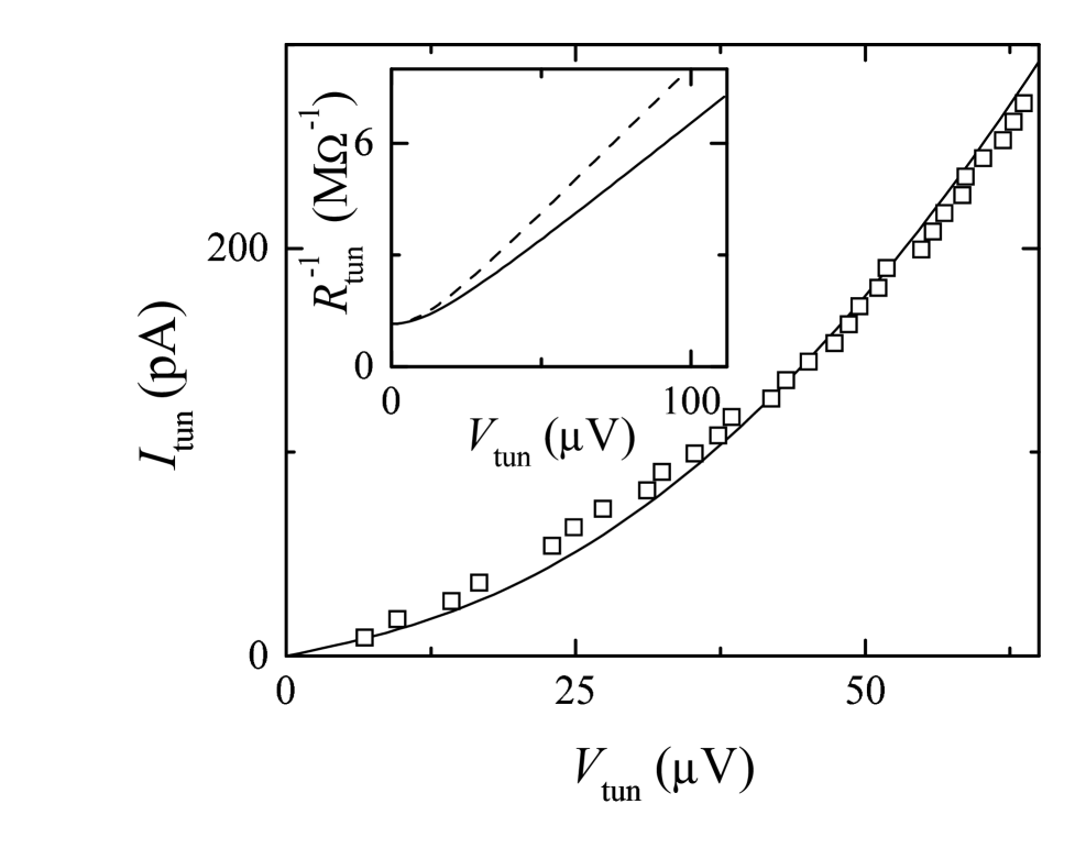
The experimental characteristics for the camel-back structure are depicted in Figs. 6 and 7. At all magnetic fields, these are parabolic at and linear at as caused by temperature smearing. The parabolic behaviour of the curves corresponds to a linear pseudogap. To describe the data we calculate the first Fourier harmonic of the voltage on the nonlinear element defined by the expression
| (6) |
where is a factor and is given by Eq. (1) with . The density of states in the back electrode is assumed to be featureless even in high magnetic fields because of the low mobility in the highly doped layer, and is the Fermi distribution function. So-calculated characteristics fit the experiment very well with only one fitting parameter (Figs. 6,7). For visualization purpose the solid line from Fig. 6 is drawn in the coordinates () in the inset to Fig. 6. Also shown by a dashed line is the corresponding dependence before filtering out the first Fourier component. One can see the finite-temperature-induced saturation of at .
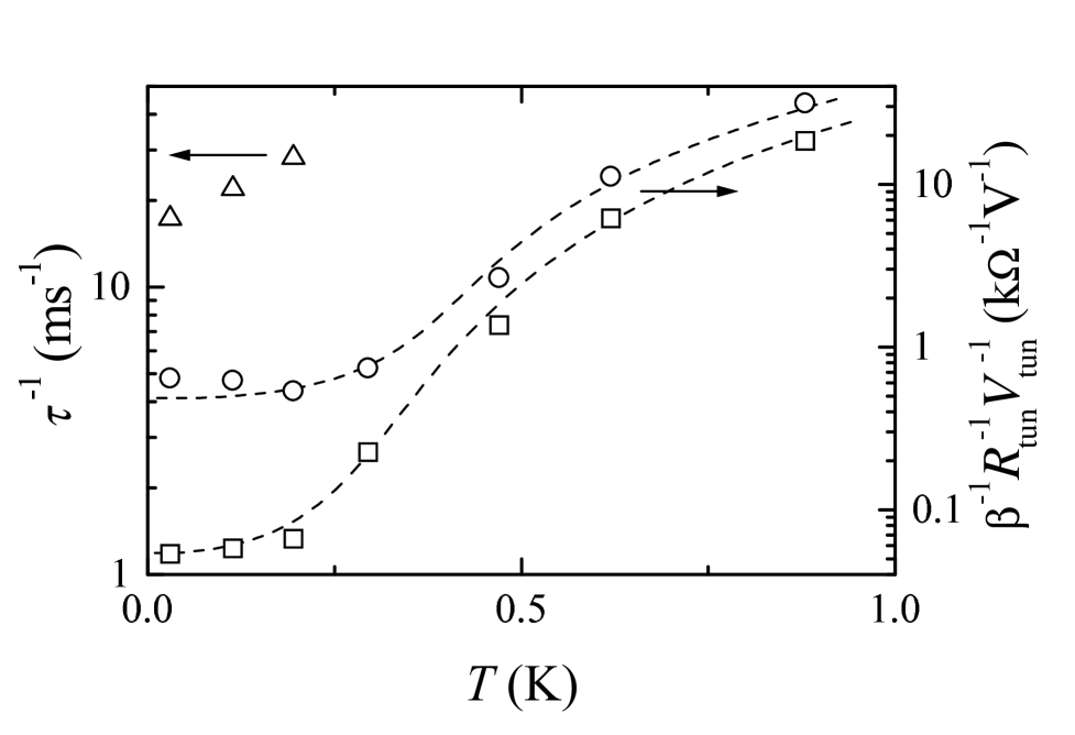
Assuming that for a given sample the values and are constant, the pseudogap parameter depends on magnetic field and temperature in the same way as the experimentally determined slope of the dependence on the parabolic part of curves, see the inset to Fig. 7 and Fig. 8. To our surprise, we find that the value changes strongly with both magnetic field and temperature. At high magnetic fields and low temperatures there is a tendency to saturation of (that the electron temperature is not saturated in the low temperature limit is indicated by the pronounced temperature dependence of the tunnel resistance at , see Fig. 8) while at low magnetic fields and high temperatures the pseudogap disappears.
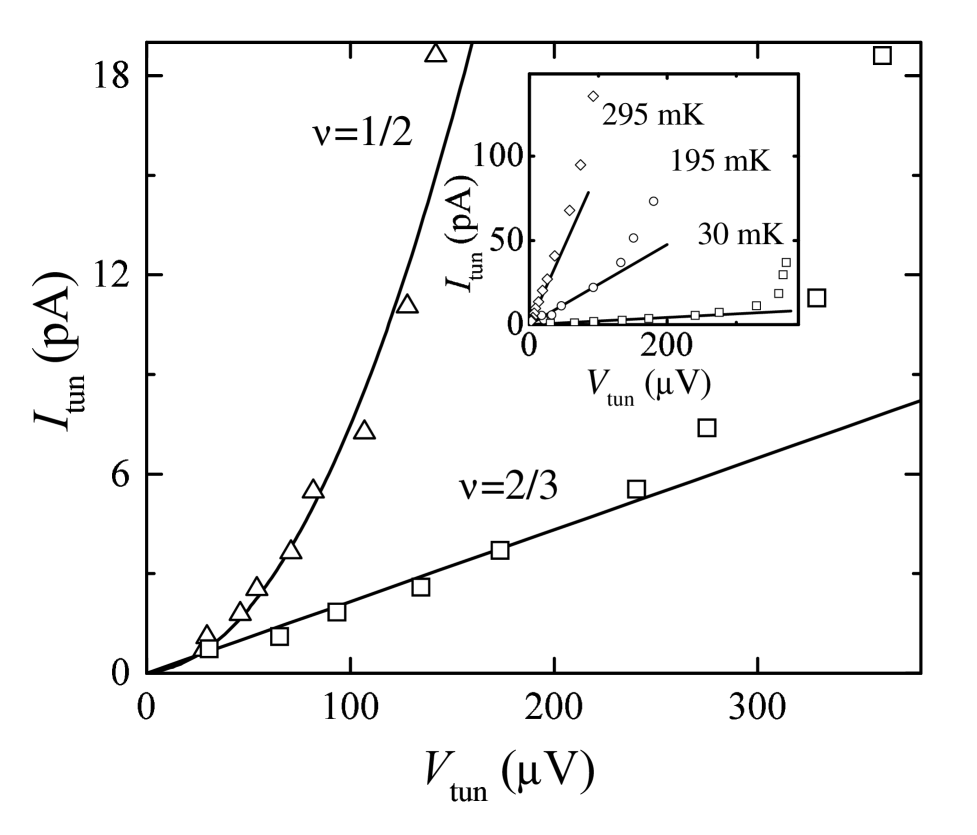
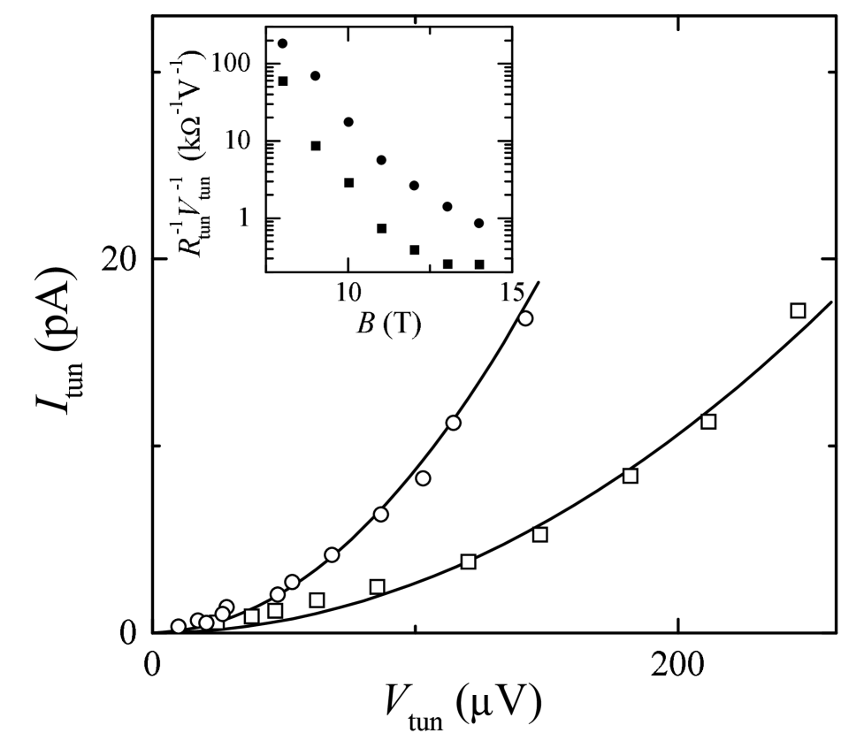
The active current component at converted into by means of Eq. (2) is displayed for different magnetic fields in the inset to Fig. 3. The relaxation time turns out to be of the same order of magnitude as the one of Ref. [7] and the slow relaxation time of Ref. [10]. Also, the magnetic field dependence of the background signal is close to that reported in Refs. [7, 8]. In contrast, peaks at filling factors and 2/3 were never observed in previous publications, we believe, because of a problem with lateral transport in Ref. [6] and too low magnetic fields used in Ref. [10]. As seen from the figure, the peak is less influenced by the background and so it is more suitable for investigations. The low temperature characteristics for the background at and for the peak are compared in Fig. 9. While the former is close to parabolic at , the current-voltage characteristic stays linear up to much higher voltages until it increases abruptly. As seen from the inset to Fig. 9, the observed linear region shrinks with temperature.
IV Discussion
In view of the existence of a pseudogap at in a 2D electron system over a wide region of filling factors, our data are consistent with results of preceding experimental and theoretical publications. We confirm that the pseudogap is linear in energy for the background at and establish that the linear law is valid also for the camel-back structure around . A linear pseudogap may be anticipated at where the localization length is expected to be small so that the limiting case of electrons localized on individual impurities is approached [14, 21]. While the theory predicts the universal pseudogap slope , we find that the parameter depends on temperature and magnetic field so that it saturates at high magnetic fields and low temperatures. In view of the fact that in this limit the electrons are best localized we may anticipate that in this limit the classical value is approached.
The characteristic dependence of the pseudogap parameter on filling factor near is reflected by the double-peak tunnel resistivity as described above. Particularly, from the analysis of curves it follows that the slope reaches a maximum at (Fig. 7). Comparison of the positions of the (or ) peaks around with the metal-insulator phase diagram obtained on samples of similar quality [24] shows that the peak position is close to the metal-insulator transition point. Hence, as the filling factor deviates from , the pseudogap parameter decreases and then passes through a minimum near the metal-insulator transition.
The theoretical models developed heretofore allow one to account qualitatively for the above behavior of with filling factor. According to Refs. [17, 18], for the metallic phase the tunneling-caused excessive charge should accommodate through the dissipative conductivity in the 2D plane. The higher the conductivity, the lower the resulting tunnel barrier because of faster charge accommodation and, therefore, the pseudogap narrows as one advances deeper into the metallic phase. As mentioned above, an exponential pseudogap is expected in the metallic phase at zero temperature
| (7) |
where is the thermodynamic density of states and is the diffusion coefficient [18, 25]. This conflict between the linear and exponential pseudogap can be sorted out as follows. An idea has been expressed in Ref. [25] that, given the average size of the conducting clusters in the insulating phase, the dependence (7) should be replaced in the energy interval by with . In agreement with our finding, the so-defined enhances at because the correlation length decreases when going deeper into the insulating phase. Following the approach of Ref. [25], for actual samples where the correlation length is always restricted one expects a linear pseudogap in the close vicinity of in the metallic phase as well. This allows reconciliation of the data at on the linear pseudogap (Ref. [7] and the present paper) and the exponential one [6, 8] as obtained in very different ranges of tunnel voltages.
Still, the temperature and magnetic field dependences of as well as the prominence of the filling factor with respect, e.g., to cannot be explained by existing theories. In the vicinity of our data indicate a decrease of the effective area that is accompanied by the emergence of another, shorter relaxation time related to the ”remaining area”, which is in agreement with results of Ref. [10]. As mentioned above, we preclude the possibility that the factor describes a macroscopic area in the sample with high tunnel resistivity because this would imply the presence of lateral transport. The origin of the effect may be different rates for tunneling into the edge and the bulk of electron islands whose size exceeds by far the magnetic length. Indeed, with decreasing the conducting clusters break up into smaller ones so that the fraction of electrons near the internal ”edges” with lower tunnel resistivity should increase reaching a maximum at . Another way of explanation is to invoke spin effects as has been suggested in Ref. [10].
Intriguingly we find a completely different behavior of the curves at fractional filling factor and 2/3 where the tunnel current rises linearly with the voltage up to a critical voltage that drops as the temperature is increased, see the inset to Fig. 9 and Fig. 41 from Ref. [26]. This is likely to point to a real gap in the 2D spectrum at fractional that collapses with temperature. We find that at the lowest temperatures the estimated gap value is close to the value obtained in Ref. [26]. So, the gaps for tunneling at and 2/3 are not manifested by double-peak structures such as at and have a different energy dependence whilst the gaps in the thermodynamic density of states at all of these filling factors look similar [12, 23].
V Conclusion
In summary, we have performed vertical tunneling measurements to investigate the Coulomb pseudogap in a 2D electron system of high-mobility (Al,Ga)As/GaAs heterojunctions subjected to quantizing magnetic fields. From the analysis of characteristics it has been found that the pseudogap is linear in energy for both the background tunnel resistance at and the camel-back structure at . The filling factor dependence of the pseudogap slope near can be explained qualitatively by theory whereas the observed change of with temperature and magnetic field is not yet clear. We give independent confirmation of the appearance at of another, shorter relaxation time for tunneling. The very different curves found at the and 2/3 peaks of the tunnel resistance are interpreted as manifestation of the fractional gap. Its estimated value and temperature behaviour agree well with results of previous studies.
Acknowledgements.
We would like to thank P. Kopietz, K.V. Samokhin, and A.V. Shitov for valuable discussions and G.E. Tsydynzhapov and I.M. Mukhametzhanov for technical assistance. Furthermore, we are very grateful to D. Schmerek and H.J. Klammer for sample preparation. The band diagram was calculated using a programme by G. Snider. This work was supported in part by the Russian Foundation for Basic Research under Grant No. 97-02-16829, the Programmes ”Nanostructures” under Grant No. 97-1024 and ”Statistical Physics” from the Russian Ministry of Sciences, and the Deutsche Forschungsgemeinschaft via the Graduiertenkolleg ”Physik nanostrukturierter Festkörper”.REFERENCES
- [1] A.M. Chang, L.N. Pfeiffer, and K.W. West, Phys. Rev. Lett. 77, 2538 (1996).
- [2] M. Grayson, D.C. Tsui, L.N. Pfeiffer, K.W. West, and A.M. Chang, Phys. Rev. Lett. 80, 1062 (1998).
- [3] A.A. Shashkin, V.T. Dolgopolov, E.V. Deviatov, B. Irmer, A.G.C. Haubrich, J.P. Kotthaus, M. Bichler, and W. Wegscheider, JETP Lett. 69, 603 (1999).
- [4] R.C. Ashoori, J.A. Lebens, N.P. Bigelow, and R.H. Silsbee, Phys. Rev. Lett. 64, 681 (1990).
- [5] R.C. Ashoori, J.A. Lebens, N.P. Bigelow, and R.H. Silsbee, Phys. Rev. B 48, 4616 (1993).
- [6] J.P. Eisenstein, L.N. Pfeiffer, and K.W. West, Phys. Rev. Lett. 69, 3804 (1992); 74, 1419 (1995).
- [7] H.B. Chan, P.I. Glicofridis, R.C. Ashoori, and M.R. Melloch, Phys. Rev. Lett. 79, 2867 (1997).
- [8] K.M. Brown, N. Turner, J.T. Nicholls, E.H. Linfield, M. Pepper, D.A. Ritchie, and G.A.C. Jones, Phys. Rev. B 50, 15465 (1994).
- [9] V.T. Dolgopolov, H. Drexler, W. Hansen, J.P. Kotthaus, and M. Holland, Phys. Rev. B 51, 7958 (1995).
- [10] H.B. Chan, R.C. Ashoori, L.N. Pfeiffer, and K.W.West, Phys. Rev. Lett. 83, 3258 (1999).
- [11] J.P. Eisenstein, L.N. Pfeiffer, and K.W. West, Phys. Rev. B 50, 1760 (1994).
- [12] V.T. Dolgopolov, A.A. Shashkin, A.V. Aristov, D. Schmerek, W. Hansen, J.P. Kotthaus, and M. Holland, Phys. Rev. Lett. 79, 729 (1997).
- [13] B.L. Altshuler, A.G. Aronov, and P.A. Lee, Phys. Rev. Lett. 44, 1288 (1980).
- [14] A.L. Efros and B.I. Shklovskii, in Electron-Electron Interaction in Disordered Systems, edited by A.L. Efros and M. Pollak (North-Holland, Amsterdam, 1985).
- [15] A.L. Efros, Phys. Rev. Lett. 68, 2208 (1992).
- [16] Y. Hatsugai, P.-A. Bares, and X.G. Wen, Phys. Rev. Lett. 71, 424 (1993).
- [17] S. He, P.M. Platzman, and B.I. Halperin, Phys. Rev. Lett. 71, 777 (1993).
- [18] L.S. Levitov and A.V. Shitov, Pis’ma Zh. Eksp. Teor. Fiz. 66, 200 (1997).
- [19] P. Johannson and J.M. Kinaret, Phys. Rev. Lett. 71, 1435 (1993).
- [20] I.L. Aleiner, H.U. Baranger, and L.I. Glazman, Phys. Rev. Lett. 74, 3435 (1995).
- [21] S.-R. E. Yang and A.H. MacDonald, Phys. Rev. Lett. 70, 4110 (1993).
- [22] F.G. Pikus and A.L. Efros, Phys. Rev. B 51, 16871 (1995).
- [23] V.T. Dolgopolov, A.A. Shashkin, A.V. Aristov, D. Schmerek, H. Drexler, W. Hansen, J.P. Kotthaus, and M. Holland, Phys. Low-Dim. Struct. 6, 1 (1996).
- [24] A.A. Shashkin, V.T. Dolgopolov, G.V. Kravchenko, M. Wendel, R. Schuster, J.P. Kotthaus, R.J. Haug, K. von Klitzing, K. Ploog, H. Nickel, and W. Schlapp, Phys. Rev. Lett. 73, 3141 (1994).
- [25] D.G. Polyakov and K.V. Samokhin, Phys. Rev. Lett. 80, 1509 (1998).
- [26] I.V. Kukushkin and V.B. Timofeev, Adv. Phys. 45, 147 (1996).