[
Non-Kondo zero bias anomaly in electronic transport through an ultra-small Si quantum dot
Abstract
We have studied low-temperature single electron transport through ultra-small Si quantum dots. We find that at low temperatures Coulomb blockade is partially lifted at certain gate voltages. Furthermore, we observed an enhancement of differential conductance at zero bias. The magnetic field dependence of this zero bias anomaly is very different from the one reported in GaAs quantum dots, inconsistent with predictions for the Kondo effect.
pacs:
PACS numbers: 73.23.Hk, 85.30.Vw, 85.30.Wx, 75.20.Hr
]
Quantum dots (QDs) formed in GaAs/AlGaAs heterostructures have been used as model systems to study transport in the Coulomb blockade regime[1]. Following advances in nanolithography QD size was reduced down to the level where quantum effects start to play a role. As the size become smaller collective phenomena, such as the Kondo effect, were recently reported[2, 3]. To further reduce the QD size for exploring new phenomena, one must abandon the conventional approach of using field–induced barriers. Recently, Si dots with confinement provided by the sharp Si-SiO2 interface have been realized. These dots can be fabricated so small that the single-electron transistor (SET) can operate at room temperature[4, 5]. Although an increase of the operating temperature of SETs was the primary driving force behind the development of the Si quantum dot technology, there were some limited studies of electron transport at low temperatures, which provided information about energy spectrum in these structures[6] and probed first-order quantum corrections to the conductivity in the Coulomb blockade regime[7].
In this paper we report low temperature electron transport in ultra–small Si quantum dots. We found that at certain range of gate voltages Coulomb blockade is lifted at K and differential conductance at zero source-drain bias increases as the temperature is lowered. Although it is appealing to attribute the enhancement to the Kondo effect, we find that the magnetic field dependence of this zero bias anomaly is inconsistent with such an interpretation.
We have investigated transport in quantum dot samples which are metal–oxide–semiconductor field effect transistors (MOSFETs) with a Si dot connected to the source and drain leads through tunneling barriers. The dot is surrounded by 40-50 nm of SiO2 and wrapped by a poly-Si gate (fabrication details can be found in Ref. [8]). The gate is also extended over the tunneling barriers and parts of the leads, adjacent to the dot. Outside the gate, the source and drain are -type. An inversion layer is formed at the Si-SiO2 interface by applying a voltage to the poly-Si gate. Unlike GaAs dots, there are no separate gates to control the coupling between the dot and the source/drain. In fact, the coupling is a function of the applied gate voltage . We studied more than 30 samples which show Coulomb blockade above 10 K. However, at low temperatures ( K) and low source–drain bias ( V) the conducting channel under the gate breaks apart and the samples have electrical characteristics of multiply–connected dots. Wide sweeps of the gate voltage are accompanied by sudden switching, which could be due to charging/discharging of some traps in the oxide. If we restrict the sweeps to V, we can obtain reproducible results for several days.
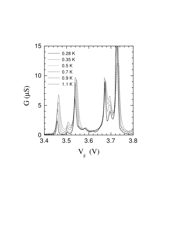
In Fig. 1 the differential conductance is plotted as a function of at a source-drain bias for six different temperatures from one of the samples. From the device geometry the dot–gate capacitance is estimated to be 1-2 aF. We attribute large peaks at , 3.54, 3.67 and 3.73 V to the main lithographically defined quantum dot. From the analysis of vs. and data we estimate gate voltage – to – single particle energy conversion coefficient mV/meV.
The in the valleys between most of the peaks is thermally activated and vanishes rapidly at low . However, in some valleys (for example between peaks at 3.54 and 3.67 V) the is almost -independent. Remarkably, in such valleys the vs. data reveals a maximum close to the zero bias in the entire range of the valley. This is in striking contrast to the broad minimum around observed in the neighboring Coulomb blockade valleys. In Fig. 2a we plot a representative vs. curve measured at V. The peak at mV has a weak dependence on the : it shifts from mV at V to mV at V. Similar results which show slightly off–zero bias peaks that shift as a function of the have been reported in GaAs quantum dots[9, 10]. In the case of the Kondo regime, the shift of the peak from can be qualitatively explained by the energy– and – dependent coupling of the dot to the leads. The maximum at mV vanishes at K and becomes a broad minimum.
This zero bias anomaly is sensitive to an external magnetic field . At T, applied parallel to the conducting channel, the enhanced conductivity is suppressed and Coulomb blockade is restored in the entire range V V. At T the conductance shows a broad minima near . In Fig. 2b we plotted vs. at for different . There is no apparent dependence of the peak position on , while the peak magnitude decreases as is increased. The peak is completely suppressed by T.

There are striking differences between the Kondo effect reported in GaAs dots and the zero bias anomaly in our data. One of the signatures of the Kondo effect is that at the zero bias peak in is split into two peaks separated by twice the Zeeman energy, . Such a splitting was reported in GaAs quantum dots[2, 3, 9] as well as in metallic grains[11]. meV at T (assuming in Si) and the splitting is expected to be mV (indicated by a bar in Fig. 2b). The width of the zero bias peak in our data is mV at T, half the expected Kondo splitting. However, we have seen no splitting of the zero bias maximum as a function of in our data up to T, the highest field at which the maximum is still observed. Also, the position of this maximum is not effected by magnetic field.
An underlying physics for the Kondo effect requires the highest occupied level in the dot to be at least doubly degenerate. Adding an extra electron to the dot costs just a bare charging energy , where is the total capacitance from the dot to the gate and leads. Adding a second electron should cost , where is due to the size quantization in the dot (or it can be the same if the level is more than two–fold degenerate). Thus, the Kondo effect is expected to be observed in the narrower valley between two adjacent charge–degenerate peaks which are separated by , while neighboring valleys are expected to be wider with gate voltage separation of . However, we observed zero bias anomaly in the widest valley with mV, while the neighboring valleys with widths 80 and 60 mV have no zero bias anomalies at . There is also a characteristic shift of the charge–degeneracy peaks as a function of temperature in the Kondo regime[12]. As temperature decreases, off-resonant conductance is enhanced which results in the shift of the charge–degeneracy peaks toward each other. Instead, we observed that the peak at V shifts to the lower gate voltages as the temperature is decreased, while the position of the peak at V is almost temperature independent.

Dependence of the conductance of the zero bias peak on , and is shown in Fig. 3. The temperature range K, where zero bias anomaly is observed, is not sufficient to extract the functional dependence with certainty, although it is close to being logarithmic. The zero bias peak is superimposed on a parabolic –dependent background, thus we cannot unambiguously conclude what is the functional dependence of on the bias voltage. In contrast, is a strong function of the magnetic field. As shown in the inset in Fig. 3, magnetic field exponentially suppresses the conductance by more than an order of magnitude. Note, that one expects a weak logarithmic suppression of by magnetic field at in the Kondo regime.
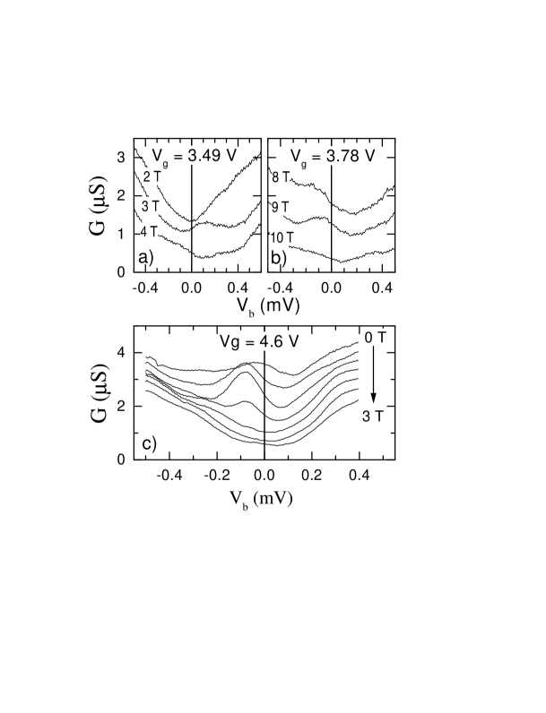
Another striking result is that in some Coulomb blockade valleys the zero bias anomaly appear only at non-zero magnetic field. These valleys may group around the valley where the zero bias anomaly is observed at . For example, at we observe a peak in at in the valley 3.54 V 3.67 V (Fig. 2), while there are broad minima at in the neighboring valleys (3.46 V 3.54 V and 3.67 V 3.72 V). The zero bias anomaly peak at 3.55 V 3.66 V is destroyed by T and has a broad minimum centered at at higher magnetic field. However, at T has a maximum in the valley 3.46 V 3.54 V. In Fig. 4a the –dependence of is shown in the center of that valley at V. While there is a minimum around at T and T, there is a pronounced peak at mV at T. In the neighboring valley (at V) we observed a peak at mV at T. At yet higher T there is a maximum at mV at V, as shown in Fig. 4b. These maxima are observed over a limited range of T.
In some Coulomb blockade valleys zero bias anomaly is observed at , although the strongest zero bias peak is found at . As shown in Fig. 4c, at V the strongest zero bias peak is at T; the peak becomes a broad minimum at T. There are no zero bias anomalies developed in the adjacent valleys in the experimental range of T.
To summarize our findings, we observed a suppression of the Coulomb blockade and an enhancement of the differential conductance at low temperatures at certain gate voltages. This anomaly is destroyed by i) raising the temperature, ii) increasing the bias, or iii) applying a magnetic field. Unlike in the Kondo effect, the zero bias anomaly in our experiment is not split by the magnetic field but, instead, the magnetic field suppresses it exponentially. Also, at certain gate voltages we observed a zero bias anomaly at . Our data cannot be understood within the framework of the theories of the Kondo effect.
Authors gratefully acknowledge discussions with Ned Wingreen. The work was supported by ARO, ONR and DARPA.
REFERENCES
- [1] L. P. Kouwenhoven, C. M. Marcus, P. L. McEuen, S. Tarucha, R. M. Westervelt, and N. S. Wingreen, in Mesoscopic Electron Transport, Vol. 345 of NATO ASI series, edited by L. L. Sohn, L. P. Kouwenhoven, and G.Schön (Kluwer Academic Publishers, Boston, 1997).
- [2] D. Goldhaber-Gordon, H. Shtrikman, D. Mahalu, D. Abusch-Magler, U. Meirav, and M. A. Kastner, Nature 391, 156 (1998).
- [3] S. M. Cronenwett, T. H. Oosterkamp, and L. P. Kouwenhoven, Science 281, 540 (1998).
- [4] L. Zhuang, L. Guo, and S. Y. Chou, Appl. Phys. Lett. 72, 1205 (1998).
- [5] H. Ishikuro, T. Fujii, T. Saraya, G. Hashiguchi, T. Hiramoto, and T. Ikoma, Appl. Phys. Lett. 68, 3585 (1996).
- [6] H. Ishikuro and T. Hiramoto, Appl. Phys. Lett. 71, 3691 (1997).
- [7] H. Matsuoka and S. Kimura, Appl. Phys. Lett. 66, 613 (1995).
- [8] E. Leobandung, L. Guo, Y. Wang, and S. Y. Chou, Appl. Phys. Lett. 67, 938 (1995).
- [9] J. Schmid, J. Weis, K. Eberl, and K. v. Klitzing, Physica B 256, 182 (1998).
- [10] F. Simmel, R. H. Blick, J. P. Kotthaus, W. Wegscheider, and M. Bichler, cond-mat/9812153 (unpublished).
- [11] D. C. Ralph and R. A. Buhrman, Phys. Rev. Lett.72, 3401 (1994).
- [12] D. Goldhaber-Gordon, J. Göres, M. A. Kastner, H. Shtrikman, D. Mahalu, and U. Meirav, Phys. Rev. Lett.81, 5225 (1998).