Polarization fields in nitride nanostructures: ten points to think about
Abstract
Macroscopic polarization, both of
intrinsic and piezoelectric nature,
is unusually strong in III-V nitrides, and
the built in electric fields in the layers of
nitride-based nanostructures, stemming from
polarization changes at heterointerfaces,
have a major impact on the properties of single and multiple
quantum wells, high mobility transistors, and thin films.
The concepts involved in the theory and
applications of polarization in nitrides have encountered
some resistance in the field. Here we discuss critically
ten “propositions” aimed at clarifying the main
controversial issues.
Keywords: III-V nitrides, spontaneous polarization, piezoelectricity, quantum wells, HEMT
pacs:
PACS nos.: 73.40.Kp, 77.22.Ej, 73.20.DxIII-V nitrides are a new frontier of semiconductor physics [1] . One of their basic properties, macroscopic polarization, offers unique opportunities for device design and basic investigations. Polarization manifests itself as built-in electrostatic fields in polarized layers interfaced to each other. These fields affect the characteristics, performance, and response of multilayer nanostructured devices. Here we discuss some theoretical basics and a number of practical implications of polarization fields for nitride nanostructures.
The microscopic foundations of dielectric polarization theory, established in the first half of the present decade [2, 3], identify the zero-field or transverse polarization of a periodic bulk crystal as the gauge-invariant Berry’s phase of its occupied Bloch orbitals, accumulated in an adiabatic transformation of the system from some reference state to its actual state [2, 3]. , which can equivalently be viewed as the integrated polarization current flowing through the crystal during the transformation, has no relation with the charge density of the polarized dielectric. Importantly, can be calculated accurately from first-principles density-functional calculations [2, 3, 4, 5, 6, 7]. The absolute polarization of a material can also be obtained by referencing its polarization to that of a system for which =0 by symmetry (for wurtzite, this may be the zincblende phase [4]). Although not directly measurable, is relevant to polarization and fields in finite, e.g. multilayer, systems through classical relations of the sort , where is the (measured or computed [5, 7]) static dielectric tensor, and is the dipole moment per unit volume of the finite system, i.e. the termination-dependent longitudinal polarization (also identified with minus the screened field generated by the net polarization charge at the sample surfaces or outer interfaces). It is simple, as discussed below, to generalize such expression to a multilayer systems relevant in technology in terms of the more fundamental only [8]. In the rest of the paper, any mention of polarization refers to the transverse variant .
In the case of III-V nitrides [9], we deal with the total polarization + () in a given strain state at zero temperature, in the absence of external fields. A key point is that in wurtzite nitrides the total polarization at zero strain, known as spontaneous, is non-zero and large. The spontaneous polarization has a fixed direction on general grounds [10], and specifically it points along (000) in III-V nitrides. The strain-induced piezoelectric term () can in principle point in any direction depending on strain. Since nitride multilayers are usually grown along the (0001) axis, () actually lies along that axis. Given the results of Ref. [4] and the conventions explained therein, for a layer under tensile strain (lattice constant must expand to fit on substrate, e.g. AlGaN on GaN) the piezoelectric polarization points along (000, whereas for a layer under compressive strain (lattice constant must contract to fit on substrate, say InGaN on GaN) it points along the (0001) direction. Similarly to , the piezoelectric component () is also quite unusually large, given the giant piezoelectric constants of III-V nitrides [4, 11].
It is clear that the two components just discussed can sum up or cancel each other out depending on strain and polarity; whether this increases or decreases the field in the layer, depends on the polarization and geometry of the neighboring layers. In fact, the polarization of a material manifests itself at the interface with a different medium as a fixed local charge accumulation. If the interface is insulating and gap-states–free (as is generally the case for the isovalent common-anion nitride interfaces), simple relations holds [6, 13] between interface charges and bulk transverse polarization. These were verified directly in ab initio calculations on interfaces of binary nitrides [5, 6] and of other materials [7]: polarization charge densities of order 1013 cm-2, localized in an interface region Å thick are found to be common. As a consequence of these large charge accumulations [14], macroscopic electrostatic fields exist in the interfaced layers, screened by dielectric response [free-carrier screening is taken up later on in the paper].
The typical effects of polarization fields are such, as discussed further below, that comparing the predictions of polarization theory with typical experiments is an inherently indirect process, requiring considerable modeling. It is essential that this modeling be done appropriately. We have previously applied [12, 13] a sophisticated (and complicated) approach to realistic nanostructures, whereby we solve selfconsistently an empirical tight-binding Schrödinger equation and Poisson’s equation. The latter reads
| (1) |
where the position-dependent quantities , , , , , and are respectively the displacement field, dielectric constant, potential, hole density, electron density, and total transverse polarization. The effects of composition, polarization, and free carrier screening are thus included in full, and non-equilibrium as well as equilibrium carrier distributions can be studied.
In this paper, instead, we discuss qualitative aspects of polarization effects referring to a simple expression for the the electrostatic field in the -th layer of a periodic but otherwise arbitrary multiple quantum well or superlattice made of layers of materials of thicknesses and dielectric constants :
| (2) |
with sums running on all layers (including the -th). is
the total,
spontaneous plus piezoelectric, transverse polarization of the material
in layer .
This expression, which can be derived
[8] under the somewhat restrictive
assumptions of
periodic boundary conditions and
no free carrier screening,
shows at a glance that polarization effects couple together
all parts of a multilayer structure via polarization differences.
Also, simply using Eq. 2 and the values calculated in
Ref. [4] for piezoconstants and intrinsic
polarization, several often-neglected facts are immediately
apparent.
1 – Spontaneous and piezoelectric
polarizations are
comparable, and neglecting either of the two components leads
to inaccuracies. This is best seen in
numerical examples; for instance,
Al0.2Ga0.8N assumed to be strained on GaN has a piezoelectric
component of –7.5 mC/m2
and a spontaneous one of –39.4 mC/m2;
an In0.1Ga0.9N layer strained on GaN
has +15.6 mC/m2 piezo, and –29.3 mC/m2 spontaneous.
This reflects directly on fields. For a
strained GaN/In0.1Ga0.9N isolated QW
(given the of GaN spontaneous polarization –29 mC/m2)
one
gets a field of 30 kV/cm on neglecting the piezo component,
while the full value is –1.63 MV/cm.
For an unstrained isolated Al0.2Ga0.8N/GaN
QW, neglect of spontaneous polarization gives a field of –1.14 MV/cm
instead of the actual –1.89 MV/cm.
The effect is less dramatic in the AlGaN/GaN systems since
the piezoconstants of AlN are extremely large so that
the piezoelectric term is sizable even at low strain.
Of course, besides
the errors it causes, neglect of either of the components is conceptually ill-founded.
2 – Only polarization differences at interfaces
are relevant. This fact is a consequence of electrostatics via
=–, it is consistent
with the tenet of basic polarization theory [2] that only
polarization differences are meaningful, and
is also borne out by Eq. 2, which is derived
under simple electrostatics assumptions.
Some workers incorrectly assumed earlier on,
that in a generic MQW
the field in the active (well) region was
given by the polarization/dielectric constant
ratio of the well material only. In the case of e.g.
a GaN-matched MQW with equally thick layers of
GaN and Al0.2Ga0.8N, this assumption leads to
predict a field of –3.2 MV/cm in the well, while
using the correct procedure the fields are, as expected,
equal and opposite in the well and barrier, and 0.74 MV/cm in
modulus.
3 – The geometry of the structure determines directly
the fields. This comes about for two reasons.
First, the field is determined by the structure geometry via
Eq. 2;
second, the field-induced potential drop changes
with layer thickness.
In a GaN-matched Al0.2Ga0.8N/GaN
system with 30 Å wells and 60 Å barriers the
field in the wells is –1.31 MV/cm with a potential drop
of 0.39 eV;
if the wells are enlarged to 60 Å, the well field is
–0.98 MV/cm, and the potential drop is –0.59 eV.
Hence, doubling the thickness of a single
layer does not straightforwardly produce a doubled
potential drop. This is most relevant since it is
just this potential drop that causes
the optical shifts visible in PL measurements.
Note in passing that the number of barrier/well units
and their growth sequence is also relevant.
4 – Piezo vs spontaneous dominance
depends on composition.
Nanostructures involving AlGaN/GaN will be dominated by
spontaneous fields, due to the huge difference in spontaneous
polarization between AlN and GaN, and their relatively small lattice
mismatch. GaN/InGaN nanostructures will be dominated by
piezoelectricity, since the spontaneous polarization
difference between InN and GaN is small, whereas
their lattice mismatch is large.
This becomes obvious considering that, in the
Vegard hypotesis, for each 10 % molar fraction change
the specific strain
is –1 % for InN in GaN, and +0.25 % for AlN in GaN, while
is +0.3 mC/m2 and –5.2 mC/m2
for the same cases.
The interplay of free carriers (intrinsic,
extrinsic, injected, photogenerated, etc.)
and polarization fields in nitride multilayers
turns out to give rise to a rich variety of new phenomena.
A closer look to these issues
through accurate simulations
and thoughtful experiments has indeed revealed several
hot spots:
5 – Optical transitions are red-shifted, slowed down,
and made less intense by the fields.
This effect, due to the progressive spatial
separation of hole and electrons at the two sides
of the QW,
was observed by several workers in strained
GaN/InGaN [15],
and strained as well as unstrained AlGaN/GaN MQWs
[16, 17]. In calculations, it was shown
that at excitation densities typical
for PL measurements, the shift in a single
QW is perfectly linear with the thickness, and
the oscillator strength is suppressed accordingly
[12, 13, 18]. The shifts are most often such that
the transition occurs well below the band gap energy.
Identifying the magnitude of the polarization via measurement of
the shifts requires an accurate modeling, expecially
when different well thicknesses are used
at the same time in a MQW [17], and also in the
small-thickness limit where the field-induced red shift
is not linear due to the competing confinement blue shift.
6 – Optical excitation, electrical injection, or doping,
lead to partial screening of the fields due to generation of
free carriers in the active layers or thereabouts. This was
observed in experiment as a blue shift
of the transition energy and recovering oscillator strength as a
function of excitation power [12, 15].
As indicated theoretically [12, 13],
the blue shift is in fact relative to the field–red-shifted energy,
and failure to recognize the red shift as due
to polarization has lead to overestimates of the In contents in
InGaN layers. Referring
to Fig. 1, more points are worth a mention.
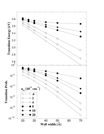
A very substantial
excitation is needed to recover appreciable oscillator strengths,
and to blue-shift the transition back towards the flat-band value;
this finding agrees with thresholds of GaN-based lasers being up to
one order of magnitude larger than in GaAs-based devices.
Further, the oscillator strength never
reaches unity, and the energy never equals the gap plus confinement
energy even in the highest power limit. This
is because the relevant length scale for free carrier
screening of the field is of order 15-20 Å due
to the larger spatial extension of the quantum-confined carriers
as compared to the polarization charge. A possible
exception are extremely
thin wells where the screening length is similar to the well width,
and the confinement blue shift competes with the field red shift.
Note that while
excitation-driven screening dies out as excitation is removed,
permanent screening can be and has been achieved by remote
doping [13, 19].
7 – The field-induced potential drop can become
similar to the gap of the layer material, for typical fields
(several MV/cm) over typical well thickness ( 100 Å).
Screening by the intrinsic
carriers becomes important in this limit. As could be guessed,
simulations show that at non-zero temperature,
as a result of free carrier generation at the opposite
ends of the sample, the field-induced potential drop across a given layer
never exceeds the gap, but rather [13]
the field obeys for
thicknesses .
Since the relevant ’s are
generally larger than typical QW thicknesses, the gap
closure regime is generally not of interest there, but it may be
to thick layers (used e.g. to measure alloy properties).
On the other hand, cases exist where intrinsic carriers
determine the boundary conditions, as in the next point.
8 – Self-doping may occur
in “constrained” systems. This was observed experimentally
by at least three groups [20, 21, 22]
and confirmed theoretically [23] in the instance of
high mobility transistors. We pick the example of a thick
( 300 Å) AlGaN layer on a very thick
( 1.5 m) GaN buffer, contacted at the top. The metal
Fermi level, the Schottky contact barriers, and the interface band
offset limit the maximum admissible potential drop through the AlGaN
layer to about 1 eV. The polarization field would instead
imply a drop of about 4
eV. For equilibrium to be established, a large part of the polarization
charge at the heterointerface must therefore
be screened by free carriers, coming in
from the GaN layer (not from the contact due to
the Schottky barrier) following the strongly attractive polarization-induced
potential drop on the GaN side. The GaN layer is typically
unintentionally doped to at least 1016 cm-3, hence a
fair source of electrons. The end result at equilibrium [20, 21, 22, 23]
is the accumulation of a
extremely high-density (up to 1013 cm-2)
two-dimensional electron gas at the AlGaN/GaN
heterointerface channel (the mechanism is
summarized, e.g., in Ref. [13] and
discussed in detail in Refs. [20], [22], and [23]).
The mobility and channel transconductance
are increased accordingly [23], also thanks
to the absence of ionized impurities in the channel itself.
Two groups[20, 21] have interpreted their results in
terms of piezoelectricity only, while a third [22]
has included spontaneous
polarization. At the level of charge density CV profiling
measurements, the uncertainties are sufficiently large, and the
interpretations indirect enough that both ways of proceeding
can get acceptable credit; as mentioned in the next point,
however, only spontaneous polarization stands the
consistency check with the sample polarity.
Two-dimensional hole gases
can also be obtained thanks to fields,
as demonstrated recently [24].
A superlattice is designed so that the field in the doped
barriers and well is equal and opposite; this is
achieved to a good approximation with a MQW with equal well
and barrier thickness ( see Eq. 2). The field enhances,
essentially by field ionization, the release of holes
from the relatively deep acceptors in the GaN or alloy
layer, and funnels the holes to the interface holding negative
polarization charge. Holes accumulate at the interface
forming a degenerate 2-D gas. Spontaneous polarization
was accounted for, and measured charge densities matched well those
predicted by modeling.
9 – Polarity plays a key role:
since the polarization in each layer has a definite sign
dictated by strain and by the spontaneous polarization direction, the
combination of polarizations to produce fields (Eq. 2) is
determined by the polarity of the structure. This is in turn
determined by the substrate- and preparation-dependent growth face
[N-face, i.e. (000) surface up, or rather Ga-face,
i.e. (0001) surface up]. Hence control on, and awareness of the
polarity issue is also essential, since
it is easy to envisage how polarity influences experiments.
The measurement of polarization effects
through field-induced optical shifts
in quantum wells is “sign-blind”, since the field sign is
immaterial to the observed
shift. In electrical devices such as HEMTs, if a charge
accumulation is expected at a given interface for a given
polarity, the occurrence of the opposite polarity will cause
instead a depletion, as displayed in Fig. 2.

Of course, the magnitude of polarizations in the layers
will determine the density of the 2-D gas, hence quantitative
agreement can be expected only including both components.
Indeed, in CV experiments on controlled-polarity
HEMT structures [22], the appearance (or non-appearance)
of a 2-D gas at a specific interface was shown to correlate
[22] with the existence of the spontaneous polarization
component, and its value was estimated in fair agreement with our
calculations [4].
10 – Piezoelectric and spontaneous polarization can be
independently controlled to a large extent, basically because only
the first depends on strain. It is easy to show [13]
that it is possible to obtain completely unstrained, yet polarized
layers, as well as strained yet unpolarized systems. In the first
case, the piezo component vanishes by construction, hence spontaneous
polarization is unambiguously the only remaining source of field, and
can therefore be measured. In the second case, the composition must be
such that polarization differences are zero across all interfaces,
whence the fields vanish in all layers. It is rather clear that,
since realizing this situation requires compensating piezo and
spontaneous components, alloying with Al and In will be
needed. For instance, the field-free case should be obtained with
GaN-matched GaN/Al0.10In0.06Ga0.84N MQWs with equally
thick wells and barriers. Also GaN-matched
GaN/Al0.68In0.32N MQWs should exhibit the same behavior.
In practice, one would measure the red shift vs. thickness
for a series of GaN/AlInGaN MQWs starting at null In content;
upon progressively increasing the In content, the shift should be
first seen to vanish, and then to reappear for larger In concentration.
Problems (or opportunities)
that should be watched out for in modeling are that
the interface band offset may switch to type-II, and that alloy
phase separation is likely.
Of course, the “critical” concentrations mentioned above
must be taken as indicative only, in view of their sensitivity
to the intricate interdependencies of strain,
lattice parameters, piezoconstants, and spontaneous polarization
values.
We thank Oliver Ambacher for discussions and for pointing out recent experimental work in the field. VF thanks the Alexander von Humboldt Foundation for support of his stays at the WSI. Support by INFM under a Section-E PAISS project is acknowledged.
REFERENCES
- [1] See the recent review by O. Ambacher, J. Phys. D: Appl. Phys. 31, 2653 (1998).
- [2] R.D. King-Smith and D. Vanderbilt, Phys. Rev. B 47, 1651 (1993); R. Resta, Rev. Mod. Phys. 66, 899 (1994)
- [3] D. Vanderbilt and R.D. King-Smith, Phys. Rev. B 48, 4442 (1993).
- [4] F. Bernardini, V. Fiorentini, and D. Vanderbilt, Phys. Rev. B 56, R10024 (1997).
- [5] F. Bernardini, V. Fiorentini, and D. Vanderbilt, Phys. Rev. Lett. 79, 3958 (1997).
- [6] F. Bernardini and V. Fiorentini, Phys. Rev. B 57, R9427 (1998).
- [7] F. Bernardini and V. Fiorentini, Phys. Rev. B 58, 15292 (1998).
- [8] F. Bernardini and V. Fiorentini, physica status solidi, in print.
-
[9]
Polarization in the nitride alloys
used in heterostructures is estimated by Vegard-like
linear interpolation between binary compound data as
for e.g. AlGaN, where the spontaneous polarization vectors, piezoelectric tensors [4], and strain fields are assumed to be known. Similar relations hold for quaternary solutions. While there is no guarantee that this Vegard-like estimate be accurate, there is no alternative to this route at this point in time.(3) (4) - [10] G. Burns, Solid State Physics (Academic Press, San Diego 1990), Sec 5.4.
- [11] K. Shimada, T. Sota, K. Suzuki, and H. Okumura, Jap. J. Appl. Phys. 37, L1421 (1998).
- [12] F. Della Sala, A. Di Carlo, P. Lugli, F. Bernardini, V. Fiorentini, R. Scholz, and J.-M. Jancu, Appl. Phys. Lett. 74, 2002 (1999).
- [13] V. Fiorentini, F. Bernardini, F. Della Sala, A. Di Carlo, and P. Lugli, Phys. Rev B. 60, in print (1999).
- [14] Not related to dangling bonds as in abrupt heterovalent junctions, and not implying interface instability [6].
- [15] T. Takeuchi, S. Sota, M. Katsuragawa, M. Komori, H. Takeuchi, H. Amano, and I. Akasaki, Jpn. J. Appl. Phys. 36, L382 (1997); S. F. Chichibu, A. C. Abare, M. S. Minsky, S. Keller, S. B. Fleischer, J. E. Bowers, E. Hu, U. K. Mishra, L. A. Coldren, S. P. DenBaars, amd T. Sota, Appl. Phys. Lett. 73, 2006 (1998).
- [16] J. S. Im, H. Kollmer, J. Off, A. Sohmer, F. Scholz, and A. Hangleiter, Phys. Rev. B 57, R9435 (1998); B. Gil, P. Lefebvre, J. Allegre, H, Mathieu, N. Grandjean, M. Leroux, J. Massies, P. Bigenwald, and P. Christol, Phys. Rev. 59, 10246 (1999); P. Lefebvre, J. Allegre, B. Gil, H, Mathieu, N. Grandjean, M. Leroux, J. Massies, and P. Bigenwald, Phys. Rev. 59, 15363 (1999).
- [17] R. Langer, J. Simon, V. Ortiz, N. T. Pelekanos, A. Barski, R. André, and M. Godlewski, Appl. Phys. Lett. 74, 3827 (1999).
- [18] L.-H. Peng, C.-W. Huang, and L.-H. Lou, Appl. Phys. Lett. 74, 795 (1999).
- [19] T. Deguchi, A. Shikanai, K. Torii, T. Sota, S. Chichibu, and S. Nakamura, Appl. Phys. Lett. 72, 3329 (1998).
- [20] E. T. Yu, X. Z. Dang, L. S. Yu, D. Qiao, P. M. Asbeck, S. S. Lau, G. J. Sullivan, K. S. Boutros, and J. M Redwing, Appl. Phys. Lett. 73, 1880 (1998)
- [21] A. D. Bykhovski R. Gaska, and M. S. Shur, Appl. Phys. Lett. 73, 3577 (1998);
- [22] O. Ambacher, J.Smart, J. R. Shealy, N. G. Weimann, K. Chu, M. Murphy, W. J. Schaff, L. F. Eastman, R. Dimitrov, L. Wittmer, M. Stutzmann, W. Rieger, and J. Hilsenbeck, J. Appl. Phys. 85, 3222 (1999).
- [23] R. Oberhuber, G. Zandler, and P. Vogl, Appl. Phys. Lett. 73, 818 (1998).
- [24] P. Kodozoy, M. Hansen, S. P. DenBaars, and U. K. Mishra, Appl. Phys. Lett. 74, 3681 (1999).