Luttinger-liquid-like transport in long InSb nanowires
Abstract
Long nanowires of degenerate semiconductor InSb in asbestos matrix (wire diameter is around 50 Å, length 0.1 - 1 mm) were prepared. Electrical conduction of these nanowires is studied over a temperature range 1.5 - 350 K. It is found that a zero-field electrical conduction is a power function of the temperature with the typical exponent . Current-voltage characteristics of such nanowires are found to be nonlinear and at sufficiently low temperatures follows the power law . It is shown that the electrical conduction of these nanowires cannot be accounted for in terms of ordinary single-electron theories and exhibits features expected for impure Luttinger liquid. For a simple approximation of impure LL as a pure one broken into drops by weak links, the estimated weak-link density is around per cm.
pacs:
PACs numbers: 73.20.Dx, 73.50.Fq,73.61.EyElectron-electron correlation effects being negligible in three-dimensional case play the dominant role in one dimension. As a result, the physical properties of a one-dimensional (1D) metal are expected to be dramatically different from properties of usual metals with a Fermi liquid of electrons. One of the main consequences of the electron-electron Coulomb repulsive interaction is the decrease of the energy density of states around the Fermi energy. The resulting electron state depends on details of electron-electron interaction. In the absence of the long-range interaction an 1D electron liquid (so-called “Luttinger liquid” [5] (LL)) is formed, whereas long-range Coulomb interaction leads to 1D Wigner crystal [6]. Transport properties of 1D electron systems are the subject of very high interest. It was shown that in Coulomb blockade systems the tunnelling transparency of a barrier vanishes due to electron-electron interaction resulting to the power-law zero-bias anomaly for the conduction [7] (see also [8]). For the particular case of LL similar result was also obtained by more strong methods [2, 3, 4, 9, 10]. A role of impurity scattering in the presence of short-range [4, 11] and long-range [10, 12] interactions was also intensively studied.
Luttinger-liquid-like behaviour for tunnelling into fractional Hall edge states predicted in [9] was recently observed in a GaAs-Al0.1Ga0.9As heterostructure in quantum Hall regime with the filling factor 1/3 [13]. However each of these edge states have properties of so-called “chiral Luttinger liquid” but not those of LL. They are similar but not identical. Luttinger-liquid behaviour was predicted also for carbon nanotubes [15, 16]. Small (below one order of magnitude) voltage and temperature variations of the conductance of single-walled nanotubes consistent with the expectations for LL were observed experimentally [14].
In the present paper we report an electric conduction of InSb nanowires in an asbestos matrix. It has been found that it follows the power law over 5 orders of conduction variation and can be described as conduction of a pure LL broken into drops by weak links, the estimated weak-link density being around per cm.
Natural asbestos is a mineral, which is very convenient for nanowire preparation. It represents itself a crystal-like package of long fiber-like tubes of roughly 300 Å in diameter with a central hole of approximately 50 Å in diameter [17, 18]. Almost any material at sufficiently high pressure and temperature can fill the holes. As the distance between nanowires is large, nanowires are independent of each other, in contrast to numerous quasi-one dimensional conductors where overlapping of wave functions of electrons on metal chains leads to 3D-ordered charge-density waves. Superconducting properties of In, Sn and Hg nanowires [19, 20, 21], weak localisation phenomena [22] and the first order melting transition in Hg nanowires in asbestos [23] were studied earlier.
In the present case of InSb as a nanowire material the asbestos was filled under the pressure 15 kbar at temperature 550 ∘C. Preliminary pumping was undertaken to evacuate gases absorbes by asbestos. In contrast to many other filling materials [19, 20, 21, 22, 23] InSb nanowires were found to be stable at room temperature even after removing the pressure.
Samples were cut from big crystals of asbestos filled by InSb. Typical sizes of studied samples are 0.01-0.1 mm for their width and thickness and 0.1-1 mm for the length along the fibers of asbestos. Thus each sample contains nanowires. We found that in most cases such samples have also longitudinal cracks filled by InSb. To eliminate the effect of such cracks the samples were etched in 1:1 mixture of HCl and HNO3 during 10-40 minutes. As such a procedure removes also InSb from the ends of asbestos filaments, the samples were shortened after etching to remove empty ends.
In most cases the current terminals were made by vacuum deposition of indium, in few cases In-Ga amalgam was used for contact preparation. We used two-terminal measurement technique for measurements of electrical conduction of both pure asbestos and InSb in asbestos. No difference was found between conduction data of samples with both types of contacts, but the vacuum-deposited ones were found to be much more stable. Electrical conduction of bulk InSb samples was measured by both 2 and 4-terminal technique. No substantial contact effects was observed. Measurements of temperature dependencies of conductance and current-voltage characteristics (I-V curves) were done in the voltage-controlled regime. Electrometric amplifier U5-11 and electrometer Keithley 617 were used for measurements of currents down to A.
We prepared and tested the room-temperature conductance of more that 80 samples of InSb in asbestos. Around 50 of them were chosen for detailed investigation of temperature and electric field conduction variation. For comparison we also measured the electrical conduction of InSb in multyfilamentary glass (vycor) with typical pore diameter around 70 Å, of bulk pieces of InSb extracted from cracks, as well as the conductance of empty asbestos.
We found that all measured samples can be divided into three groups in accordance with temperature evolution of their conductance. The first group consists of samples with . Practically all non-etched samples with vacuum-deposited contacts belong to this group. For such samples a rapid initial decrease of upon cooling saturates at some temperature so that their low-temperature is much similar with of a bulk InSb. We concluded therefore that in such samples the dominant contribution into low-temperature conduction is provided by InSb-filled longitudinal cracks of asbestos. The second group is formed by samples whose conductance has strong temperature dependence down to the lowest temperature of measurements (1.5 K). From our point of view the conductance of these samples is provided by InSb nanowires in an asbestos matrix. The physical properties of such samples are the main subject of the present paper. In addition, some samples have very low room-temperature conductance (around Ohm-1) and very strong temperature dependence of conductance which goes out of the range of the present measurements ( Ohm-1) at temperatures below 100 - 200 K. We believe that InSb nanowires in such samples are not continuous. The properties of such samples are out of the scope of the present paper. In addition, the conductance of some samples was found to be not stable and switches between two or more different conducting states belonging to one of the conduction groups described above. Such samples do not provide any new information, and the temperature evolution of their conductance will not be described below.
Current-voltage characteristics of samples of the second group are highly nonlinear in entire temperature range studied. We also found that application of a sufficiently large voltage may irreversibly modify the shape of I-V curve, a result of such modification being dependent on a particular sample. Conduction of some samples was stable at voltages up to 30 V, but only 3 V was enough to irreversibly modify the conduction of other samples. Both irreversible increase and decrease of conduction were observed. The physical reasons for such irreversible behaviour may be related with electromigration of impurities. The data reported below were obtained for the reversible part of I-V curves.
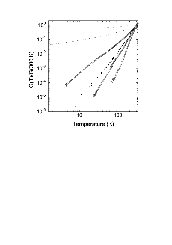
Fig. 1 shows typical dependencies of the linear conductance as a function of temperature for a representative set of samples of InSb-filled asbestos. The typical room-temperature resistance of such samples is 10 kOhm - 10 MOhm. of InSb from extracted from a crack in asbestos (dashed line at Fig. 1) and InSb in vycor (dotted line at Fig. 1) are shown on the same plot for comparison. First of all, of all samples was at least three orders of magnitude smaller than the conduction of a bulk InSb from a crack multiplied by the filling factor of asbestos Å Å and conduction of InSb in vycor. Secondly, the temperature dependence of their conductance was much stronger. The most remarkable feature is approximately linear shape of in log-log scale (see Fig. 1). It means that . A large group of studied samples (six samples) has . Apart of this group one sample has , and another one has .
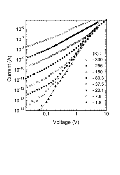
Fig. 2 gives a typical temperature set of I-V curves. The I-V curves are nonlinear at any temperature. The nonlinearity is getting more pronounced with lowering temperature. The power law, , with fits the low-temperature data over 7 orders of the current variation. Other samples reveal similar behavior with . Only a small nonlinearity (10% ) was observed for InSb in vycor at K for electric fields V/cm .
The doping level of InSb from cracks in asbestos is expected to be close to one of InSb in nanowires. The weak temperature dependence of conduction of a bulk InSb indicates that InSb nanowires are made of a heavy-doped degenerate InSb with the carrier concentration above cm-3. Qualitative difference between the temperature dependencies of the conductance of InSb in vycor glass and InSb nanowires indicates dramatic changes in the physical properties of InSb nanowires due 1D character of electron states, rather than the finite-size effect only. For an InSb wire with a diameter Å and the current carrier’s effective mass the energy separation between the first and the second quantum levels for the examined temperature range. So the electron band structure of 50 Å InSb nanowires is essentially one-dimensional. Other details of the band structure are not very certain. In particular, the Fermi energy depends on uncertain parameters and . If cm-3, then , i.e. there is a single quantum conduction channel.
Thus the studied samples consist of long quantum wires with one or few quantum conduction channels. The wires are made of degenerate semiconductor and contain large amount of impurities and defects. Single-electron 1D variable-range hopping conduction apparently does not fit the data. In principle, with are known for charge-limited injection currents in semiconductors and dielectrics [24]. Similar dependencies were really observed by us for empty asbestos, as well as for asbestos with broken nanowires, with . As for InSb nanowires, observed for some samples is out of the range for the current-injection case [24].
is predicted for tunnelling between two drops of pure LL [2, 3, 4], for LL in a long wire with impurities [1], and for 1D Wigner crystal [10]. Similarly, is predicted for tunnelling between two drops of pure LL [2, 3, 4], for LL in a long wire with impurities [1], and for Coulomb blocade effect [7, 8, 12]. However the dependence is predicted for tunnelling of 1D Coulomb gas [25], Wigner crystal [26, 27], and for a pure LL in the presence of long-range Coulomb interaction [25]. We suppose that in our multiwire samples long-range interactions may be screened and the system behaves itself more like LL. Tendency to Anderson localisation caused by backward scattering on impurities is essentially reduced due to repulsion of electrons [11]. Hence in our opinion all properties of the system are stipulated by two basic factors: i) by the power-like behaviour for “pseudo-gap” for density of states near the Fermi level, ii) by the presence of weak links in each wire.
So the power laws for both and are predicted for a weak link between two pure LL [2, 3], as well as for impure LL [1] approximated here as drops of LL connected through weak links in serial. For a sample consisting of identical quantum wires with independent weak links in each and [2, 3] can be rewritten as
| (1) |
and
| (2) |
where , is a measure of tunnelling transparency of -th weak link, is an energy scale for LL, and and , where and are bare and renormalized [1] dimensionless constants ( for a pure LL [2, 3]).
Observed values are 2.3 and 2.3, 3.4 and 4.4, 4.5 and 3.8, 4.6 and 3.0 for and respectively. corresponds to that is considered as a typical value for LL theory [2, 3]. If , and all weak links are identical, can be estimated from Eqs. (1),(2) without fitting parameters from comparison of I-V curves and . For the sample with one gets , that corresponds to weak links/cm per a wire. Taking for other samples K and experimental values A, 1/Ohm, one gets respectively. The respective weak link density per a wire is around per cm.
Two kinds of contact effects are expected to affect the transport properties of quantum wires. The first one caused by electron reflection from the contact can be described as an additional contact resistance of the order of kOhms [28] per each quantum wire. This contribution is negligible in the low-temperature region. The second one associated with interaction of electrons with image charges induced in the contacts leads to potential redistribution along a nanowire [29, 30]. In accordance with [29, 30] at sufficiently low temperatures even in the case of a quantum wire with a single barrier the major contribution comes from the barrier rather from the contact effect. This is even more true for our multibarrier samples.
So LL theory provides plausible explanation of our experimental data. We would like to note that LL is mostly a convenient theoretical approximation: long-range Coulomb interaction, backscattering and interference effects yield modification of the theory. There are reasons to expect that more realistic description of InSb nanowires may be possible without substantial modification in and .
Three of us (S.V.Z.-Z., Yu.A.K., and Yu.A.F) are grateful to C.R.T.B.T.-C.N.R.S. for hospitality during the initial stage of the research. We would like to thank S.N. Artemenko and V.Ya. Pokrovskii for their interest to this work, and A.M. Nikitina for assistance in sample etching. This work has been supported by C.N.R.S. through jumelage 19 between C.R.T.B.T. and IRE RAS, the Region Rhone-Alpes through the programme Tempra, the Russian Foundation for Basic Research (grants 97-02-18267, 98-02-16667), and MNTP “Physics of Solid State Nanostructures” 96-2008 and 97-1052.
REFERENCES
- [1] Renn, S.R. & Arovas, D.A., “Nonlinear characteristics of Luttinger liquids and gated Hall bars”, Phys. Rev. B 51, 16832-16839 (1995).
- [2] Kane, C.L. & Fisher, M.P.A.,“Transport in a One-Channel Luttinger Liquid”, Phys. Rev. Lett. 68, 1220-1223 (1992).
- [3] Kane, C.L. & Fisher, M.P.A., “Transmission through barriers and resonant tunnelling in an interacting one-dimensional electron gas”, Phys. Rev. B46, 15233-15262 (1992).
- [4] Furusaki, A. & Nagaosa, N, “Single-barrier problem and Anderson localization in a one-dimensional interacting electron system”, Phys. Rev. B 47, 4631-4643 (1993).
- [5] Haldane, F.D.M.,“ ‘Luttinger-liquid theory‘ of one-dimensional quantum fluids: I. Properties of the Luttinger model and their extension to the general 1D interacting spinless Fermi gas”, J. Phys. C: Sol. St. Phys. 14, 2585-2609 (1981).
- [6] Schultz, H.J., “Wigner Crystal in One Dimension”, Phys. Rev. Lett. 71, 1864-1867 (1993).
- [7] Girvin, S.M., Glasman, L.I., Jonson, M., Penn, D.R., & Stiles, M.D., “Quantum fluctuations and the single-Junction Coulomb blocade”, Phys. Rev. Lett., 64, 3183-3185 (1990).
- [8] Matveev, K.A., Yue, Dongxiao & Glasman, L.I., “Tunneling in One-Dimensional Non-Luttinger Liquid”, Phys. Rev. Lett. 71, 3351-3354 (1993).
- [9] Wan, X.-G., “Edge transport properties of the fractional quantum Hall states and weak-impurity scattering of a one-dimensional charge-density wave”, Phys. Rev. B 44, 5708-5719, (1991).
- [10] Maurey, H. & Giamarchi, T., “Transport properties of a quantum wire in the presence of impurities and long-range Coulomb forces”, Phys. Rev. B 51, 10833-10843 (1995).
- [11] Giamarchi, T. & Schultz, H.J., “Anderson localization and interactions in one-dimensional metal”, Phys. Rev. B 37, 325-340 (1988).
- [12] Maurey, H., & Giamarchi, T., “Coulomb blockade in a quantum wire with long-range interactions”, Europhys. Lett. 38, 681 (1997).
- [13] Chang, A.M., Pfeiffer, L.N., & West, K.W., “Observation of Chiral Luttinger Behavior in Electron Tunneling into Fractional Quantum Hall Edges”, Phys. Rev. Lett., 77, 2538-2541 (1996).
- [14] Bockrath, M., Cobden, D.H., Lu, J., Rinzler, A.G., Smalley, R.E., Balents, L., & McEuen, P., “Luttinger-liquid behaviour in carbon nanotubes”, Nature, 397, 598-601 (1999).
- [15] Egger, R. & Gogolin, A., “Effective low-energy theory for correlated carbon nanotubes”, Phys. Rev. Lett., 79, 5082-5085 (1997).
- [16] Kane., C., Balents, L., & Fisher, M.P.A., “Coulomb interactions and mesoscopic effects in carbon nanotubes”, Phys. Rev. Lett., 79, 5086-5089 (1997).
- [17] Pundsak, F.L., “The pore structure of chrysotile asbestos”, J. Phys. Chem., 65, 30-33 (1961).
- [18] Yada, K., “Study of chrysotile asbestos by a high resolution electron microscope”, Acta Cryst. 23, 704-707 (1967).
- [19] Bogomolov V.N. & Kumzerov, Yu.A. “Fluctuations in mercury filaments five atoms in diameter” JETP Lett., 21, 198-200 (1975);
- [20] Bogomolov, V.N., Klushin, N.A. & Kumzerov, Yu.A., “Superconducting transition in indium filaments at 6K”, JETP Lett.,26, 72-74 (1977);
- [21] Bogomolov, V.N., Kolla, E.V. & Kumzerov, Yu.A., “One-dimensional effects in low temperature conductivity of ultrathin metallic filaments”, Sol. St. Commun., 46, 383-384 (1983).
- [22] Bogomolov, V.N., Kolla, E.V. & Kumzerov, Yu.A., “Determination of the critical temperature of the ultrathin metals filaments superconducting transition and its dependence on the filament diameter”, Sol. St. Commun., 46, 159-160 (1983).
- [23] Bogomolov, V.N., Kolla, E.V. & Kumzerov, Yu.A., “First-order phase transition in approximately one-dimensional system”, JETP Lett., 41, 34-37 (1985).
- [24] Lampert, M.A. & Mark, P., “Current injection in solids”, Acad. Press, New York and London, 1970.
- [25] Nagaosa, N. & Furasaki, A., “Tunneling through barrier in Coulomb gas confined in quantum wire”, J. Phys. Soc. Japan 63, 413-415 (1994).
- [26] Glazman, L.L., Ruzin, I.M. & Shklovskii, B.I., “Quantum transport and pinning of a one-dimensional Wigner crystal”, Phys. Rev. B 45, 8454-8463 (1992).
- [27] Fabrizio, M., Gegolin, A.O. & Schedel, S., “Coulomb effect in transport properties of quantum wires”, Phys. Rev. Lett. 72, 2235-2238 (1994).
- [28] Maslov, D.L. & Stone, M., “Landauer conductance of Luttinger liquid with leads”, Phys. Rev. B 52, 5539-5542 (1995).
- [29] Sablikov, V.A. & Shchamkhalova, B.S., “Electron transport in a quantum wire with realistic Coulomb interaction”, Phys.Rev. B 58, 13847-13855 (1999).
- [30] Egger, Reinhold & Grabert, Hermann, “Applying voltage sourses to a Luttinger liquid with arbitrary transmission”, Phys. Rev. B 58, 10761-10768.