Theoretical study of the reconstruction of -SiC(001)
Abstract
By means of ab initio molecular dynamics and band structure calculations, as well as using calculated STM images, we have singled out one structural model for the reconstruction of the Si-terminated (001) surface of cubic SiC, amongst several proposed in the literature. This is an alternate dimer-row model, with an excess Si coverage of , yielding STM images in good accord with recent measurements [F.Semond et al. Phys. Rev. Lett. 77, 2013 (1996)].
pacs:
73.20.At,68.35.BsThe reconstructions of SiC(001) surfaces have been widely studied in the last ten years[2], the characterization and understanding of growth mechanisms on the (001) substrate being prerequisites for technological applications. In the case of Si-terminated surfaces, several reconstructions have been found to occur; , and periodicities have been observed in LEED[3, 4, 5], RHEED[6] and STM[7, 8, 9, 10, 11, 12] measurements. Both (21) and c(42) reconstructions pertain to a complete Si monolayer at the top , as clearly indicated by all available experimental data[5, 6]. Unlike those of Si(001), the reconstructions of SiC(001) are characterized by weakly bonded, flat dimers ((21) [13, 14]) or by alternating symmetric dimers with different heights (c(42)[14, 15, 16]). Adsorption of additional Si produces successive reconstructions as a function of Si coverage, including , , and a combination of and periodicities[5, 6, 7, 9, 11, 12].
The reconstruction seems to be the last stage before self-limitation of growth[17]. Its atomic configuration and electronic structure are not clearly established, though they have been intensively investigated. Three different atomic configurations, depicted on Fig. 1, have been suggested in the literature. In the Double Dimer-Row (DDR) model, proposed by Dayan[3] and possibly supported by other experimental studies[7, 12, 18, 19], there are two Si ad-dimers on top of the full Si layer (Fig. 1.a). The resulting coverage is in contradiction with the measured value of reported by several groups[5, 6, 17]. The straightforward extension of this model to the reconstruction is also inconsistent with the measured coverage[6]. Moreover, this model is not supported by some STM studies[8, 9]. The DDR is favored by empirical molecular dynamics (MD) simulations[20], but the Tersoff potential used in these calculations is known to give a poor description of -SiC surface reconstructions[21]. Another model, the ADDed dimer-row (ADD), was first suggested in an early study by Hara et al[5]. This configuration, with one Si ad-dimer per unit cell (Fig. 1.b), corresponds to the measured coverage for the and reconstructions. However, though it appears consistent with several experimental data, both empirical[22] and ab initio[23] calculations have shown that it is not energetically favored. Furthermore, STM investigations do not support this model[7, 8]. Another coverage model, the ALTernate dimer-row (ALT) (Fig. 1.c), was proposed by Yan et al[22, 23]. This configuration is supported both by calculations[22, 23] and by STM studies[8, 9]. However, it cannot account for the observed relation between single domain LEED patterns with and periodicities[2, 4]. It also fails to explain the reconstruction observed after O or H adsorption[3, 7]. Note that all three models involve Si ad-dimers which are perpendicular to the dimers on the underlying Si surface. Indeed, previous calculations have shown that a single parallel ad-dimer is energetically much less favored than a perpendicular one[24].
All three models show some discrepancies either with existing experiments or calculations, but none of them can be safely ruled out, owing to the lack of consistency between all available data. In this contribution, we report the results of self-consistent ab initio total energy calculations for all of the three structural models, including full geometrical optimizations. The surface energies are compared using Grand Canonical Potentials. The computed dispersion of electronic states, as well as STM images, are compared to experiments. Considering all the evidence, we conclude that the reconstruction of the Si-terminated surface of SiC(001) is best described by the ALT model.

Our calculations were performed at within the Local Density Approximation, using ab initio molecular dynamics codes employed in previous studies of SiC surfaces[14]. Fully nonlocal norm-conserving pseudopotentials were used for Si (s and p nonlocality) and C (s nonlocality)[25]. The system was simulated by a slab in a periodically repeated supercell. The bottom layers were frozen in the p configuration determined earlier[14]. Two different sets of calculations have been performed. To determine the relaxed surface atomic structures, we used a supercell with 8 atomic layers and a 10 Å vacuum region (the total number of atoms is 176 (184) for ALT and ADD (DDR) models). The plane-wave energy cutoffs for the wave functions and the charge density were 36 Ry and 130 Ry, respectively. Sums over occupied states were performed at the point, which corresponds to 4 inequivalent k-points in the Brillouin Zone (BZ) for a cell. Next, the electronic band structure was computed in a supercell with 12 atomic layers and a 6 Å vacuum region, using an extension of ab-initio MD codes to finite wave functions vectors, and keeping all atoms fixed. Atomic positions in the six top layers and the two bottom layers were taken from the preceding ab-initio MD calculations, whereas those in the four central layers were assumed bulk-like. Wave functions and charge densities were expanded in plane waves with cutoffs of 40 Ry and 160 Ry, respectively. In these calculations, the electronic charge density was computed using 8 special k-points in the BZ, generated according to the Monkhorst-Pack scheme[26].
The relaxed atomic structures for the three models are shown on Fig. 1. In the DDR geometry, one ad-dimer is strongly tilted ( Å) and has a short bond length ( Å) while the other, weakly bound ( Å), is almost flat ( Å). The inequivalence of the two ad-dimers disagrees with simple expectations[3, 7] and with previous calculations by Kitabatake et al, who found two flat ad-dimers for the DDR model[20]. Their use of the Tersoff potential could explain this disagreement, owing to the neglect of charge transfer between Si and C atoms. A single flat and weakly bonded ad-dimer ( Å) is obtained in the ADD model, the geometry being close to that previously obtained by Yan et al in a calculation similar to ours[23]. Note that two slightly different configurations are possible within the same model, since the weakly bonded Si dimers in the underlying layer can be arranged either all on one side, as originally proposed by Yan et al[22, 23], or in a staggered pattern (see Fig. 1). Starting from different configurations, our calculations always converged to the staggered pattern[27]. Finally, in the ALT model, the ad-dimer is strongly tilted ( Å) and strongly bound ( Å), in good agreement with previous calculations[23]. The length of the weak Si dimers in the underlying surface layer is close to the value computed for the reconstruction using the same method and a supercell[14].
In order to determine the most stable configuration, we have compared total energies. The ALT model is lower in energy than the ADD model by about 0.5 eV per cell; this energy difference is clearly in favor of the ALT, our error bar being 0.3 eV, as estimated from cutoff and BZ sampling tests. The drastic reduction from the 3.6 eV energy difference quoted by Yan et al[23] is likely due to their poorer BZ sampling and, to a lesser extent, to the additional relaxation leading to the staggered pattern. A direct comparison with the DDR model is not possible since the corresponding Si coverage is different. This difficulty can be overcome by using the grand canonical scheme[28]. The computed surface energy differences as a function of the Si chemical potential are shown in Fig. 2. The value of for bulk silicon was calculated with an energy cutoff of 40 Ry and 32 special k-points in the BZ, whereas we used the heat of formation of SiC eV from a recent calculation[29], to obtain the Si chemical potential under C-rich conditions. Since growth is likely to occur under Si-rich conditions, a precise determination of is required only in that limit. Our results show that the ALT model is the most stable configuration over the entire allowed range of Si chemical potential. However, the energy difference between ALT and DDR obtained under Si-rich conditions is only 77 meV, i.e. within our error bar. Consequently, the DDR model can not be definitely ruled out solely on the basis of total energy comparisons.

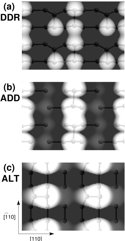
Several experimental STM studies of the reconstruction are currently available[7, 8, 30, 31]. In order to compare the three different models, we have calculated filled states constant-current STM images within the Tersoff-Hamann approximation[32]. Representative images are shown in Fig. 3. In both the DDR and ADD models we find strings of peanut-shaped spots, originating from a slight overlap between maxima on adjacent flat ad-dimers. For the DDR model, additional maxima are located on the up adatoms of the tilted ad-dimers. The resulting images are incompatible with the experimental observations of a single oval spot stretched in the direction per cell. On the other hand, in the ALT model the spread out stretched spots located above up adatoms of the tilted ad-dimers are in accord with experimental STM images of filled states[8].
Additional insight can be obtained from analysis of the electronic states within a few eV of the Fermi level. All photoemission measurements agree about the presence of two occupied surface states in the band gap, 1 eV apart from each other[19, 33, 34]. However, uncertainties exist about the location of these states with respect to the Valence Band Maximum (VBM). Recent angle-resolved photoemission spectroscopy (ARPES) measurements have shown that the dispersion of all identified surface states is very small ( eV) along the [19] and [19, 34] directions. Only the surface states of the DDR and ALT models have been considered here, the ADD model being higher in energy than the ALT model and exhibiting STM images which do not agree with experiment.
We find that in the DDR model the surface is metallic, within the Local Density Approximation. The highest occupied state, about 1 eV above the VBM at , is mainly localized on the flat ad-dimer and has a character with respect to the dimer axis. Its dispersion is very small along the direction ( eV), but rather strong along the direction ( eV). In the DDR model, we also find three additional surface states with energies between the highest occupied state and the VBM. Only one of them is localized above the up adatom of the tilted ad-dimer, and is essentially dispersionless. The other two states originate from backbond and dimer states of the underlying surface, and show strong dispersions. The presence of dispersive states in the band gap is in disagreement with ARPES evidence and points against the DDR model.
In the ALT model, the surface is semiconducting, with a direct gap at of about 0.5 eV. The highest occupied state, 0.8 eV above the VBM at , is localized on the up adatom of the tilted ad-dimer and has a strong ‘s’ character. This surface state has a small dispersion along both and directions ( eV). Close to the VBM we find another state, lying 0.7 eV below the highest occupied orbital. It is a state localized on the Si-Si dimer of the underlying surface which are not bonded to ad-dimers, and is nearly dispersionless ( eV). This state is only present in the direction. Except for the energy difference between the two highest surface states (0.7 eV vs. 1 eV), agreement with ARPES experiments is definitely better for the ALT than the DDR model.
A discrepancy exists about the number and location of occupied surface states or resonances[19, 34]. Yeom et al[19] argued that there should be a total of four states with pronounced surface character in their proposed DDR geometry. However, they considered the ideal non-relaxed geometry, with flat ad-dimers only, and, more importantly, they ignored backbond states and dimer-like states on the underlying surface which are also expected to exhibit surface character. These additional resonant states could be difficult to resolve because some are close in energy, and might have weak photoemission intensities. In our calculation we could identify resonant states, however we did not attempt to systematically analyse their character and dispersion.
Turning to unoccupied states, we find only one surface state in the band gap for the DDR model. It lies 2 eV above the VBM at , is localized around the down adatom of the tilted ad-dimer and has a predominant ‘pz’ character. Its dispersion is about 0.1 eV (0.4 eV) along the () direction. For the ALT model, two empty surface states have been identified. The lowest one, with energy 1.2 eV above the VBM at , is a -like state on the lone Si dimer of the underlying surface. It disperses about 0.1 eV along and 0.7 eV along . The other one, 1.8 eV above the VBM, is a ‘pz’-like state on the down adatom of the tilted ad-dimer and has a very weak dispersion along both directions ( eV).
The combination of all our results indicates that the ALT model is the most suitable candidate, since it explains the large majority of available measurements. The ADD and DDR models produce incorrect STM images. The ADD is energetically unfavorable, while the dispersion of the surface states calculated for the DDR model is not compatible with ARPES measurements.
To summarize, we have performed plane-wave pseudopotential calculations for three structural models of the reconstructed -SiC(001) surface. In particular, relaxed atomic structures, surface energies, STM images, surface states and their dispersion have been calculated and compared with experiments. Our results strongly favor the ALT model and exclude the DDR and ADD models, although some ambiguities remain. More definitive conclusions could come from additional experimental studies, in particular investigations of unoccupied electronic states, and a convincing confirmation of the Si coverage corresponding to the reconstruction.
We are thankful to V. M. Bermudez, P. Soukiassian, G. Dujardin and H.-W. Yeom for fruitful discussions and/or preprints. One of us (L.P.) gratefully acknowledges Prof. H.-J. Güntherodt for the facilitities provided in his group, and the Swiss National Foundation for financial support under the NFP 36 program “Nanosciences”. This work has also been partially supported by the ”Consiglio Nazionale delle Ricerche” (Italy) and the Swiss Center for Scientific Computing (Manno, Switzerland). Part of this work was performed by the Lawrence Livermore National Laboratory under the auspices of the U. S. Department of Energy, Office of Basic Energy Sciences, Division of Materials Science, Contract No. W–7405–ENG–48.
REFERENCES
- [1] Corresponding author. Present Address: Lawrence Livermore National Laboratory, Livermore, CA 94551, USA.
- [2] For a recent review, see V. M. Bermudez, Phys. Stat. Sol. (b) 202, 447 (1997).
- [3] M. Dayan, J. Vac. Sci. Technol. A 4, 38 (1985).
- [4] R. Kaplan, Surf. Sci. 215, 111 (1989).
- [5] S. Hara et al., Surf. Sci. Letters 231, L196 (1990).
- [6] T. Yoshinobu et al., Appl. Phys. Lett. 59, 2844 (1991).
- [7] S. Hara, S. Misawa, S. Yoshida, and Y. Aoyagi, Phys. Rev. B 50, 4548 (1994).
- [8] F. Semond et al., Phys. Rev. Lett. 77, 2013 (1996).
- [9] P. Soukiassian, F. Semond, A. Mayne, and G. Dujardin, Phys. Rev. Lett. 79, 2498 (1997).
- [10] V. Y. Aristov, L. Douillard, O. Fauchoux, and P. Soukiassian, Phys. Rev. Lett. 79, 3700 (1997).
- [11] L. Douillard, V. Y. Aristov, F. Semond, and P. Soukiassian, Surf. Sci. Letters 401, L395 (1998).
- [12] J. Kitamura et al. (unpublished).
- [13] J. Powers, A. Wander, M. vanHove, and G. Somorjai, Surf. Sci. Lett. 260, L7 (1992).
- [14] A. Catellani, G. Galli, F. Gygi, and F. Pellacini, Phys. Rev. B 57, 12255 (1998).
- [15] P. Soukiassian et al., Phys. Rev. Lett. 78, 907 (1997).
- [16] L. Pizzagalli et al., Thin Solid Films 318, 136 (1998).
- [17] S. Hara et al., Surf. Sci. 273, 437 (1992).
- [18] H. W. Yeom et al., Phys. Rev. B 56, R15525 (1997).
- [19] H. W. Yeom et al., Phys. Rev. B 58, 10540 (1998).
- [20] M. Kitabatake and J. E. Greene, Appl. Phys. Lett. 69, 2048 (1996).
- [21] M. Tang and S. Yip, Phys. Rev. B 52, 15150 (1995).
- [22] H. Yan, X. Hu, and H. Jónsson, Surf. Sci. 316, 181 (1994).
- [23] H. Yan, A. P. Smith, and H. Jónsson, Surf. Sci. 330, 265 (1995).
- [24] A. Catellani, G. Galli, and F. Gygi, Appl. Phys. Lett. 72, 1902 (1998).
- [25] D. Hamann, Phys. Rev. B 40, 2980 (1989).
- [26] H. J. Monkhorst and J. D. Pack, Phys. Rev. B 13, 5188 (1976).
- [27] Staggered underlying dimers induce a slight rotation of the ad-dimers towards the [110] direction. This resulting surface stress can be removed if one considers a staggered arrangement with mirror symmetry in the plane containing the ad-dimers, leading to a reconstruction. This geometry lowers the energy of the ADD model, but not enough to compete with the ALT model.
- [28] G.-X. Qian, R. M. Martin, and D. J. Chadi, Phys. Rev. B 38, 7649 (1988).
- [29] J. E. Northrup and J. Neugebauer, Phys. Rev. B 52, R17001 (1995).
- [30] S. Hara et al., Surf. Sci. 357-358, 436 (1996).
- [31] S. Hara et al., Surf. Sci. 421, L143 (1999).
- [32] J. Tersoff and D. R. Hamann, Phys. Rev. B 31, 805 (1985).
- [33] M. L. Shek et al., J. Vac. Sci. Technol. A 12, 1079 (1994).
- [34] M. Lübbe et al., J. Vac. Sci. Technol. A 16, 3471 (1998).