[
Equilibrium shapes and energies of coherent strained InP islands
Abstract
The equilibrium shapes and energies of coherent strained InP islands grown on GaP have been investigated with a hybrid approach that has been previously applied to InAs islands on GaAs. This combines calculations of the surface energies by density functional theory and the bulk deformation energies by continuum elasticity theory. The calculated equilibrium shapes for different chemical environments exhibit the {101}, {111}, {1̄1̄1̄} facets and a (001) top surface. They compare quite well with recent atomic-force microscopy data. Thus in the InP/GaInP-system a considerable equilibration of the individual islands with respect to their shapes can be achieved. We discuss the implications of our results for the Ostwald ripening of the coherent InP islands. In addition we compare strain fields in uncapped and capped islands.
pacs:
PACS numbers:68.65.+g, 68.35.Md, 68.55.-a]
I INTRODUCTION
It was observed about ten years ago that during the hetero-epitaxial growth of lattice-mismatched semiconductors small dislocation-free islands can form.[1, 2, 3, 4, 5] To emphasize the zero-dimensional character of their electronic density of states, these objects have been labeled quantum dots. Since then, the quantum dots have attracted an enormous interest in the area of semiconductor physics.[6] Besides being fascinating objects for basic research, there are also various potential applications, ranging from improved device properties of quantum-dot semiconductor-lasers, which have in fact already been demonstrated,[7] up to more exotic applications as part of a quantum computer.[8] The “self-organized” hetero-epitaxial growth of arrays of quantum dots with a preferentially narrow size distribution is thus the aim of intense research. To finally be able to optimize the growth parameters, a detailed knowledge of the growth mechanism, its energetics and its kinetics, is essential.
There is general agreement about the main driving force for, e.g., InAs/GaAs or InP/GaInP island formation in the Stranski-Krastanov growth-mode. The growth begins with the deposition of a highly strained two-dimensional film, the wetting layer. With the addition of more material beyond a critical thickness the film becomes meta-stable. Coherent, i.e., dislocation-free islands form due to the energy gained by strain relaxation in the islands. However, the details of the growth mechanism[9] are not yet well understood. In fact, there are competing theories, which are based on energy ground-state considerations on the one hand, or on kinetic, i.e. non-equilibrium effects on the other.[10, 11, 12, 13, 14] Accordingly, the final destiny of the islands, as predicted by the various theories, is rather different. The more conventional fate of the islands would be to undergo Ostwald ripening,[15, 16] i.e., the larger islands would grow at the expense of the smaller ones. The resulting island size distribution would be rather broad. In fact, for the systems of concern in our study, Ostwald ripening takes place at a slower rate than the growth rate of the islands. Kinetic effects could be active that effectively decrease the growth rate of the larger islands, thus sharpening the size distribution.[11, 12, 17] In contrast to these growth scenarios, Shchukin et al.[18, 19] have suggested that there exists a range of parameters for which islands of a finite size are thermodynamically stable. Our ab initio results for the surface energies and surface stresses, however, indicate that neither in the case of InAs/GaAs nor InP/GaInP would this mechanism result in the formation of stable islands.
For the most widely studied system of InAs islands on GaAs, a range of growth parameters seem to have been established for producing islands of certain uniform densities and a rather narrow size distribution,[21, 22, 23, 6] although these growth parameters are still subjects of discussion in the literature. Spectroscopic studies of the islands, after they were capped by barrier materials, have been reported.[24, 25, 26, 27, 28] To investigate the equilibrium shape and stability of the coherent strained InAs islands at low island densities, we have applied a hybrid method to calculate the total energy.[29, 30, 31] In this approach the energy gained by island formation is decomposed in the following form:
| (1) |
where is the gain in deformation energy when the material forms a strained island instead of a biaxially strained film, is the cost in surface energy due to the creation of facets on the sides of the island instead of the surface covered by the base of the island, and is the energy cost for the creation of sharp edges. For an isolated island to form at all in preference to a film, must be negative. The surface energy is calculated ab initio, applying density-functional theory (DFT). In Ref.[30] the surface energies corresponded to those of unstrained surfaces. This approximation was subsequently improved upon in Ref. [31], in which the renormalization of the surface energies due to surface stress was taken into account. However, the corrections amounted to a reduction of the surface energies by at most 11 % and left the prediction for the equilibrium shape qualitatively unchanged. Furthermore, the edge energy was estimated to be negligible, provided the island size is not too small. The elastic strain field can be treated within a continuum approach. Thus is calculated within linear elasticity theory using a finite-element method (FEM). The effect of nonlinearity was seen to be small.
As a result, we obtained a volume-dependent optimum shape for the InAs islands, which can be described as a (001)-truncated pyramid with {101}, {111}, and {11̄1} faces. However, the diversity of experimentally observed island shapes appears not to be reconcilable with the assumption of thermodynamic equilibrium. Among the experimental results, the mostly square-based islands have faces {101},[23] {105},[33] {113},[21] {136},[34] and a series of islands of low aspect ratios whose morphologies change according to the coverage.[22] We take this difference as an indication that a sensitivity to growth conditions and kinetic effects have to be featured in a growth theory, including the possibility that the deposited material may migrate or segregate as witnessed in the growth of quantum wells,[35, 36] and self-organized islands.[37, 38, 39]
While the predictions of the hybrid method for the equilibrium shape of InAs/GaAs coherent islands have not been borne out so far in experiment, i.e., in the ‘window’ of growth condition assumed, the experimental characterization of the three-dimensional islands in the InP/GaInP system,[17] briefly summarized in the next paragraph, seems to indicate a better chance for an equilibrium approach to be valid. Therefore, InP/GaInP represents an excellent benchmark system to show both the applicability of the hybrid method and the notion that the shape equilibration of coherent islands can be achieved.
The growth of InP/GaInP by metal-organic vapor phase epitaxy (MOVPE) has consistently yielded uncovered islands [17] that are significantly larger ( nm2) than their counterparts in InAs/GaAs ( nm2) grown by molecular beam epitaxy (MBE). Transmission electron microscopy (TEM) and atomic force microscopy (AFM) have yielded strong evidence that they have facets of low Miller indices only,[40, 41] rather reminiscent of the previous prediction for InAs/GaAs. They are stable against annealing [17] of several minutes at the growth temperature of 580 ∘C, and their morphology has been reported to remain unchanged after overgrowth with capping material.[42] Although for these materials there is a lack of specific observations of segregation inside the islands and diffusion between the islands and the barrier, it is probable that both takes place. To what extent they affect the shape and size of InP/GaP islands remains to be determined. It is also becoming clear that the spectroscopy of the islands depends not only on the volume but also significantly on the strain distribution inside the islands, and the latter is greatly influenced by the shape of the islands.[43, 44] The results for InP/GaInP complement those for InAs/GaAs, e.g., growth of quantum wells on InP islands, [45] growth characteristics,[40, 46, 47, 48, 49] photoluminescence,[45, 46, 50, 51, 52, 53] optical gain and lasing,[54] InP islands used as stressors to induce quantum dots in a quantum well,[55, 56, 57] Landau levels formation in InP islands,[58] theoretical study of the electronic states of the islands.[44, 59]
We are thus encouraged to conduct a study of InP/GaInP-islands parallel to our previous work for InAs/GaAs, and hence enlarge our general understanding of coherent strained islands. Furthermore, gaining an insight into the strain distribution of capped islands would help towards a better understanding of the potential experienced by the electrons and holes at the quantum dot and in its vicinity. Of course, if the effect of phase segregation inside the island or diffusion of atoms to and from the barrier turns out to be substantial, our approach would need to be generalized. In any event, our findings could still be used as the starting point for a yet more realistic modeling.
The organization of the work is as follows: First, we present the DFT results for the surface energies. In Section III, we describe briefly our FEM simulations and derive the equilibrium shape. We shall indicate how Ostwald ripening emerges from our model, assuming that no other faster kinetic processes have preempted its time development. In Section IV we compare the strain distributions of uncapped and capped islands. The implication for the use of strained islands as a stressor for quantum wells will be pointed out. A generalization from InP/GaP to InP/GaxIn1-xP islands, i.e., to systems with a different lattice mismatch, is included in the final Section V.
II SURFACE ENERGY
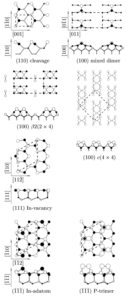
As in the case of InAs we assume that the relevant surface reconstructions, i.e., those of lowest energy, correspond to the low-index surface orientations {110},{100},{111}, and {1̄1̄1̄}. The details of the calculation of surface energies by DFT are described in Refs. [29, 31]. We apply the local density approximation to the exchange-correlation energy-functional and use ab initio norm-conserving, fully separable pseudopotentials. The plane-wave expansion of the wave function has an energy-cutoff of 10 Ry, and the k-summation makes use of a uniform Monkhorst-Pack mesh with a density equivalent to 64 k-points in the complete surface Brillouin zone of the (100) surface. We neglect the correction of the surface energies due to strain, as, for the InAs/GaAs-islands, we found it to be small and not affecting our conclusions concerning the island shape and stability.[31]
The surface atomic structures for different surface orientations are shown in Fig. 1.
The corresponding surface energies as a function of the phosphorous chemical potential are shown in Fig. 2, where the left and right vertical dashed lines mark the limits for In- and P-rich environments, respectively. They are characterized by the coexistence of the InP surface with either an In or a P bulk phase.

Since epitaxial growth takes place mostly in a P-rich environment, we list in Table I the surface energies of the stable reconstructions for the chemical potential eV. It will be shown in Section V that the experimentally observed coherent islands are best compared with the theoretical results at this chemical potential.
There are a great deal of similarities between InP and InAs surfaces in equilibrium[60, 30, 31] and some interesting differences. Both the (110) and (111) surface energies are independent of the phosphorous chemical potential. The relaxed cleavage surface and the stoichiometric In vacancy structure are the stable reconstructions for the (110) and (111) orientations, respectively. The surface energies are 55 and 62 meV/, respectively. These are to be compared with those of InAs of 41 and 42 meV/. The cleavage surfaces of the (110) orientation in InP have been observed experimentally using low-energy electron-diffraction [61] (LEED) and for both InP and InAs using low-energy positron-diffraction.[62] A DFT study of InP(110) surface has also been carried out.[63] We find the equilibrium structure of the (1̄1̄1̄) surfaces to be the same as for InAs. On the (1̄1̄1̄) surface in P-rich environment, the P-trimer reconstruction is preferred, i.e., within some interval near the right-hand dashed line in Fig. 2.
| orientation | reconstruction | surface energy |
|---|---|---|
| [meV/] | ||
| (110) | cleavage | 55 |
| (100) | 62 | |
| (111) | In-vacancy | 62 |
| (1̄1̄1̄) | P-trimer | 44 |
At eV the InP (1̄1̄1̄) surface energy is 44 meV/ compared to 36 meV/ for InAs. A reconstruction of the (1̄1̄1̄) surface [64] seems not relevant for our present study, as the area on side faces of the island might be too small to accommodate this reconstruction without having to invoke edge effects.
The (100) reconstructed surfaces of InP and InAs had been generally assumed to be similar, too. However, recent DFT studies and experimental observations by several groups using low-energy electron diffraction (LEED), reflection anisotropy spectroscopy (RAS), soft x-ray photoelectron spectroscopy (SXPS), and scanning tunneling microscopy (STM) have yielded evidence that there is a qualitative difference between the atomic structure of the InP and the InAs(100) surfaces.[65, 66, 67] In a very P-rich environment, i.e., at rather close to , DFT predicts the reconstruction to be more stable than the reconstruction, which is not the case for InAs. For InP in moderately P-rich and InAs in As-rich environments, is the common stable reconstruction. However, in an In-rich environment InP displays a mixed dimer reconstruction, in contrast to the reconstruction for InAs. However, for the growth of strained islands in a moderately P-rich atmosphere, it is still the reconstruction that is selected as in InAs/GaAs, with the surface energy equal to 62 meV/ compared to 44 meV/ for InAs.
III EQUILIBRIUM ISLAND SHAPES
For a fixed volume of the island (or, equivalently, a fixed number of atoms), the equilibrium shape minimizes the total energy of the system, of Eq. (1), with respect to all possible shapes. As explained above, the surface energy is calculated for the unstrained surface and the edge energy is neglected.[31] For a square-based island bounded solely by the four {101} surfaces, the length of the base is chosen equal to 12.9 nm and the height to 6.5 nm. This determines the volume that remains unchanged for all calculated islands. The island dimensions vary only moderately for truncated islands bounded by the other low-index surface planes we have included in this study. By construction the islands are placed 40 nm apart, and reside on a substrate of thickness 24 nm. As in the case of InAs,[30, 31] the thickness of the wetting layer has been set to zero.
We have used the commercial product MARC [68] to perform the finite-element simulations. One notable feature of all commercial products is that the preferred finite element (FE) is an eight-node hexahedron or three-dimensional arbitrarily distorted cube. It has been shown that it is superior to the simple tetrahedron in terms of fast convergence and computing speed. We have also adopted this class of FE for all our calculations, with the understanding that corners of the hexahedron can merge to form wedge-shaped or pyramid-shaped elements.
Throughout this work we have taken InP to be the island and wetting layer material, and GaP to be the barrier material, or the substrate when the island is uncapped. The corresponding experimental lattice constants and elastic moduli [69] are listed in Table II.
| Å | [GPa] | [GPa] | [GPa] | |
|---|---|---|---|---|
| InP | 5.87 | 102 | 58 | 46 |
| GaP | 5.45 | 141 | 63 | 72 |
The lattice mismatch is . Although this mismatch is quite large, we restrict ourselves to linear elasticity theory. Taking the elastic moduli from Table II, the deformation energy per unit volume of the biaxially strained uniform InP film amounts to 3.0 meV/.
In our FEM calculations of the number of FE varies slightly, depending on the island’s bounding surfaces. The number of FE is increased in the areas where the deformation energy density is large until a 1 % accuracy is achieved. In general, there are approximately 7000 FE in total, of which approximately 2000 are distributed in the island. For volume-conserving truncated islands, the elastic energy can be accurately approximated from the untruncated value by an analytical formula.[30]
The anisotropy of the surface energy driving the formation of particular crystal facets is an essential aspect of our approach.[70] We have investigated island shapes which are bounded by the low Miller-index surfaces described in Section II. The collection of shapes we have considered is the same as in the study of the InAs islands.[30, 31] The island base has the orientation (001) and the top of the island may be truncated by a plane of the same orientation (see Fig. 6 of Ref. [31]).
The results of energy evaluated according Eq. (1) are summarized in a scale-invariant manner in Fig. 3, where the ordinate and abscissa .

We have taken the surface energies at the phosphorous chemical potential = eV. The solid symbols denote untruncated islands for which a full FE calculation has been carried out. Qualitatively these results are similar to those of InAs/GaAs.[30, 31] We find that a square-based island with {101}-facets only (solid square) has a larger bulk deformation energy than a square-based island with two {111}- and two {1̄1̄1̄}-facets (rhombus). The latter has steeper side facets which allow a more efficient stress relaxation. The line that emanates from each of the solid symbols joins up the small dots for which was derived from the analytical approximation for the volume-conserving truncated island. For a given volume , islands with the same total energy lie on the straight line
| (2) |
plotted as a dashed line in Fig. 3. (Note that the edge energies have been neglected.) It is clear from Eq. (2) that the volume of the island is related to the negative slope of the line. For a given volume , the equilibrium shape of the island is determined by the first point of contact from below of the straight line, Eq. (2), with the calculated island-energy curves.
For a given island shape, and scale like and , respectively.This means that the data in Fig. 3 are invariant against a change of the volume of all islands by the same factor. However, the slope of the straight line, Eq. (2), changes, and hence a different equilibrium shape will be selected. By inspection, the results of Fig. 3 indicate that for larger V, i.e., smaller negative slope, untruncated islands are most likely to be selected, while smaller favors truncated islands as equilibrium shape. The interplay of and in Eq. (1), and how their relative weightings change as a function of the island volume have been discussed and supported by explicit calculations in Ref. [30]. Fig. 3 serves as a compact way of encapsulating the result for the equilibrium shapes for arbitrary volumes, provided that the volume (or the number of atoms) of the island is not too small to invalidate our hybrid ansatz, Eq. (1), or too large such that the island is no longer coherent (dislocations appear).
We display in Fig. 4 examples of equilibrium shapes for three different island volumes.
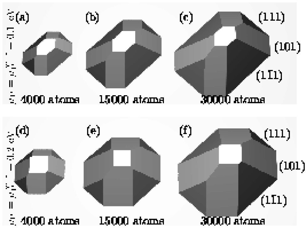
They illustrate nicely that for a smaller volume a relatively larger amount of material is truncated from the top of the island. Additionally, we can also inspect the difference in shapes due to a variation of the chemical potential: The {11̄1}-facet, which is favored in a P-rich environment, is consistently more prominent for = eV than for = eV. The equilibrium shapes shown in Fig. 4 have much similarities with the experimentally observed islands,[40, 41] in particular all observed facets are well accounted for by our theory. Note that the experiments have been carried out for InP/GaInP instead of InP/GaP, thus the experimental and theoretical lattice mismatch differ by nearly a factor of two. However, as will be discussed below, this can be accounted for by a simple re-scaling of the island volumes.
In the theory of Shchukin et al,[18] a combination of material parameters determines whether thermodynamic equilibration drives the system towards a stable array of islands or whether Ostwald ripening occurs. A stable array would arise, if in Eq. (1) is modified by the surface strain in such a way that it changes sign. Making use of our quantitative surface energies, we can estimate, whether this condition is likely to be fulfilled in case of InP or not.
The change in surface energy is given by a sum over all facets of the island:
| (3) | |||||
| (4) |
and denote the areas of the base and the -th facet on the surface of the island, respectively, is the angle between the -th facet and the substrate surface, and is the ratio of projected onto the base and . The are the surface energies from Table I. Each term within the summation of Eq. (4) is positive, and hence is positive. This has the consequence that, for a fixed equilibrium island shape, the volume derivative of Eq. (2) is always negative, i.e., the total energy per unit volume decreases as the volume increases, thus favoring larger and larger islands, leading to Ostwald ripening. To change the sign of the respective individual contribution to Eq. (4), a strain-induced renormalization of the surface energy of approximately 20 % for the facets with (101) and (1̄1̄1̄) orientations, and 40 % for the facet with (111) orientation would be necessary. For the case of InAs/GaAs, the renormalization amounted to at most 11 %. [31] Therefore, it seems reasonable to argue that Ostwald ripening is also the fate of the InP islands. Furthermore, a majority of the InP islands are grown on GaInP-substrates whose lattice mismatch is about 50 % smaller than in the InP/GaP system. This further diminishes the importance of the renormalization of the surface energy due to the strain field. Altogether this discussion seems to indicate that we are outside the parameter range for which arrays of stable islands occur. It is worth noting that the parameter range that conforms to Shchukin et al,[18] implies that in Eq. (1) changes sign due to stress, i.e., one has the unusual situation that there is a gain in total energy by creating new surfaces. Furthermore, Shchukins model includes edge energies and island-island interaction to prevent the islands from coalescing. In comparison, a new method[20] to tackle this problem of the stability of the islands has a much less restrictive ansatz and the agreement with experiments is encouraging.
IV COMPARISON OF UNCAPPED AND CAPPED ISLANDS
In this section we compare the strain fields for capped and uncapped islands. It is well documented that during overgrowth of GaAs over InAs islands there is significant migration of atoms as well as change in the morphology of the islands,[37, 39] and that In segregates during the overgrowth of GaAs over InGaAs islands or quantum wells. [35, 36, 38, 72, 73, 74] A well-studied sample of InP strained islands was grown on InGaP lattice-matched to a GaAs substrate. [40, 42] These InP islands seem quite stable - when uncapped, they survive a few minutes of annealing at 580 ∘C without changes and retain their shapes after overgrowth. These may be signs that the MOVPE-grown InP islands are less affected by atom migration and In segregation during overgrowth than the MBE-grown InAs islands. Therefore, until more specific observations of these effects are available, it would be interesting to compare the strain distributions of uncapped and capped islands without taking into account any change of shape or In segregation. While we are aware that the present results may be subjected to revision, we shall discuss below some rather general effect of the capping layer on the strain distributions.
We have adopted the shape and size of the island that had been observed by Georgsson et al,[40] displayed in their Fig. 1, i.e., a truncated pyramid grown on the (001) plane, with the defining planes for the side walls being (011), (101), (11̄1), (01̄1), (1̄01), and (1̄11). The base is elongated in the [110] direction and has a length of 66 nm, a width of 40 nm in the [1̄10] direction, and the height is 18.4 nm. The island resides on a 0.6 nm thick wetting layer. By construction the nearest-neighbor islands are 140 nm apart along the [110] and [1̄10] directions. The size of our cell is chosen large enough such that away from the island and the wetting layer the barrier material is not significantly strained. Since the island has reflection symmetry across two planes, only one quarter of the unit cell needs to be explicitly considered in the simulation. In the case of the uncapped island we have used in total 1872 FE, while for the capped island we used 3756 FE. Our simulation of InP/GaP is not exactly a reproduction of the InP/GaInP coherent island in Ref. [40], because the lattice mismatch of the latter was smaller, . We discuss the scaling with respect to the lattice mismatch at the end of this section.
We display in Fig. 5 two views of the trace of the strain tensor field, , for an uncapped island.
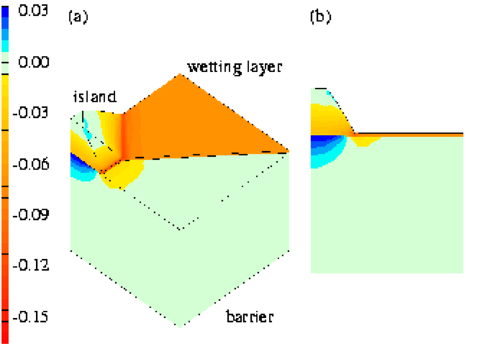
In Fig. 5 (a) a part of the wetting layer has been peeled off to reveal the strain distribution in the substrate. Qualitatively the results are quite similar to those for InAs/GaAs without the wetting layer. [31] One notes that the unhindered relaxation of the island in the upward direction has produced a small area of tensile strain at the top of the island. This seems to be a common result in all our calculations, whether the island is truncated or not. In the substrate, the strain distribution is characterized by compressive strain around the edges of the island, and tensile strain directly underneath the island. Such contrasting strains created by coherent strained islands of InP have been utilized as stressor to achieve three-dimensional quantum confinement [55, 56, 57] in sub-surface quantum-well structures, and a theoretical strain analysis similar to ours by FEM has been reported. In this discussion, an InGaAs quantum well (QW) is sandwiched between GaAs, with self-organized InP islands grown on top. The strain distribution thus produced modulates the conduction band of the QW, and creates a potential well. Photoluminescence spectra of this type of potential well have been measured and analyzed, hence this object has also earned the label of quantum dot.
For comparison we display in Fig. 6 two views of a capped InP island.
In Fig. 6 (a) part of the capping material is removed to reveal the island and the wetting layer. Part of the latter is also peeled off to show the substrate underneath. The island in this instance is entirely under compressive strain. [75] The area of tensile strain previously found in the substrate directly underneath the uncapped island has been replaced by an area of compressive strain. Small pockets of tensile strain are to be found in the vicinities of sharp corners in the capping layer. The disappearance of the pocket of tensile strain in the substrate has great significance for the creation of quantum dots in QWs as described above. The amount of capping material affects the strain-induced potential well in the QW. This phenomenon is quite general and not limited to strained InP islands. If we assume that the strain interaction is given by a ‘hydrostatic’ potential, i.e., , our present calculation shows the extreme case of destroying this potential well completely.
A closer examination of the components , , and directly underneath the island reveals that and , are tensile and remain qualitatively unchanged whether the island is capped or not. On the other hand, is slightly tensile for the uncapped island and overwhelmingly compressive for the capped island. These mechanical responses seem understandable. For capped or uncapped islands the cause of the biaxial tensile strain in the substrate perpendicular to the [001] direction is the same. However, the uncapped island heaves up in the [001] direction because the relaxation in this direction is unhindered. For the capped island, the capping material prevents the unrestrained heaving in the [001] direction. Hence the island exerts a considerable pressure onto the substrate as well, i.e., material in the substrate is compressed. Therefore the thickness of the capping layer has a great influence on the strain in the substrate.
V DISCUSSION
The experimental data on the growth of InP islands mostly involve InP grown on GaInP lattice-matched to a GaAs substrate. [40, 41, 46, 47, 48, 49, 50, 51, 52, 53, 54] In the cases where InP islands were used as stressors of QWs, they were grown on GaAs. In all these cases the lattice mismatch amounts to about . TEM and AFM have been used to characterize the coherent strained InP islands and their lateral sizes are usually found to be roughly 40 nm 60 nm and the height between 15 nm to 20 nm.
In our study we have assumed a GaP substrate with a lattice mismatch of . Therefore, our data have to be rescaled before comparing our equilibrium shapes to the experimental observations. The equilibrium shape at a given volume and lattice mismatch is calculated by minimizing the total energy with respect to the island shape . As above, we omit the contribution from the edge energy and the renormalization of the surface energy due to the strain, and make use of the scaling behavior of the elastic energy and surface energy ,
| (5) | |||||
| (6) |
where and are constants of proportionality that depend only on the shape. The total energy of the equilibrium island follows from
| (8) | |||||
Therefore the optimum island shape is the same for volumes and lattice mismatches , respectively, provided that the relation
| (9) |
holds. This simple relation will be altered, however, if the different elastic moduli for GaP and GaInP are taken into account.
Let us select from Fig. 4 the theoretical equilibrium island shape pertaining to the chemical potential = eV, and volume , because it bears the closest resemblance in shape to the island examined by AFM in Ref. [41]. We assume the volume of the latter to have the dimension given in Section IV, i.e., . Therefore, for an island of volume , formed with a mismatch of , to transform to an island of volume , the mismatch, as given by Eq. (9), ought to be . In view of all the uncertainties this appears to be reasonable. Note that the interdiffusion of In and Ga from the InP island and GaInP substrate, would decrease the assumed lattice mismatch of , hence worsening the agreement with our estimate, and would also alter the effective elastic moduli of the island and barrier materials. Although this topic has yet to be explored in these materials, there is clear evidence [74] for In and Ga interdiffusion in the growth of As islands embedded in GaAs. A quantitative clarification of interdiffusion seems to be crucial for a better understanding of the equilibrium shape and stability of the strained islands. In principle, a concentration profile or phase separation in the island can be incorporated into the FEM calculation.
In conclusion, we have reported an application of the hybrid method to study the equilibrium shape of coherent strained islands of InP on GaP or GaInP substrates. Our results are in qualitative agreement with experiments, in that all the observed facets are accounted for by our theory. We take this as an encouraging evidence that the coherent InP islands most often observed in experiments are close to local thermodynamic equilibrium. This is in contrasts to the apparent discrepancy between the calculated and observed island shapes for the InAs/GaAs islands. In view of the distinct variety of observed InAs island shapes this discussion points towards the importance of kinetic effects as the missing ingredient of a more comprehensive theory for those islands. The contribution of the surface energies to the total energy of an InP island is positive, and it seems unlikely that the sign of this contribution would change, if effects due to surface stress and strain were included. Thus our results favor the Ostwald ripening of the islands (as opposed to the creation of a thermodynamically stable array of islands). Finally, we have compared the strain fields of uncapped and capped islands. The capping material distinctly affects the strain fields in the substrate. This is of relevance for quantum dots induced in quantum wells by stressors.
Acknowledgements.
This work was supported in part by the Sfb 296 of the Deutsche Forschungsgemeinschaft.REFERENCES
- [1] D. J. Eaglesham and M. Cerullo, Phys. Rev. Lett. 64, 1943 (1990).
- [2] Y.-W. Mo, D. E. Savage, B. S. Swartzentruber, and M. G. Lagally, Phys. Rev. Lett. 65, 1020 (1990).
- [3] S. Guha, A. Madhukar, and K. C. Rajkumar, Appl. Phys. Lett. 57, 2110 (1990).
- [4] C. W. Snyder, B. G. Orr, D. Kessler, and L. Sander, Phys. Rev. Lett. 66, 3032 (1991).
- [5] B. G. Orr, D. Kessler, C. W. Snyder, and L. Sander, Europhys. Lett. 19, 33 (1992).
- [6] D. Bimberg, M. Grundmann, and N. N. Ledentsov, Quantum Dot Heterostructures (Wiley, Chichester, UK, 1998).
- [7] N. Kirstaedter, N. N. Ledentsov, M. Grundmann, D. Bimberg, V. M. Ustinov, S. S. Ruvimov, M. V. Maximov, P. S. Kop’ev, Z. I. Alferov, U. Richter, P. Werner, U. Gösele, and J. Heydenreich, Electronics Letters 30, 1416 (1994).
- [8] P. Zanardi and F. Rossi, Phys. Rev. Lett. 81, 4752 (1998).
- [9] R. Heitz, T. R. Ramachandran, A. Kalburge, Q. Xie, I. Mukhametzhanov, P. Chen, and A. Madhukar, Phys. Rev. Lett. 78, 4071 (1997).
- [10] C. Priester and M. Lannoo, Phys. Rev. Lett. 75, 93 (1995).
- [11] Y. Chen and J. Washburn, Phys. Rev. Lett. 77, 4046 (1996).
- [12] D. E. Jesson, K. M. Chen, and S. J. Pennycock, MRS Bulletin 21, 31 (1996); Phys. Rev. Lett. 80, 5156 (1998).
- [13] H. T. Dobbs, D. D. Vvedensky, A. Zangwill, J. Johansson, N. Carlsson, and W. Seifert, Phys. Rev. Lett. 79, 897 (1997).
- [14] J. Tersoff, Phys. Rev. Lett. 81, 3183 (1998).
- [15] W. Ostwald, Z. Phys. Chem. 34, 495 (1900).
- [16] M. Zinke-Allmang, L. C. Feldman, and M. H. Grabow, Surf. Sci. Rep. 16, 377(1992).
- [17] W. Seifert, N. Carlsson, M. Miller, M.-E. Pistol, L. Samuelson, and L. R. Wallenberg, Prog. Cryst. Growth Charact. Mater. 33, 423 (1996).
- [18] V. A. Shchukin, N. N. Ledentsov, P. S. Kop’ev, and D. Bimberg, Phys. Rev. Lett. 75, 2968 (1995).
- [19] I. Daruka and A.-L. Barabási, Phys. Rev. Lett. 79, 3708 (1997).
- [20] L. G. Wang, P. Kratzer, M. Scheffler, and N. Moll, Phys. Rev. Lett., in print.
- [21] J. M. Moison, F. Houzay, F. Barthe, L. Leprince, E. André, and O. Vatel, Appl. Phys. Lett. 64, 196 (1994).
- [22] D. Leonard, K. Pond, and P. M. Petroff, Phys. Rev. B 50, 11687 (1994).
- [23] S. Ruvimov, P. Werner, K. Scheerschmidt, U. Gösele, J. Heydenreich, U. Richter, N. N. Ledentsov, M. Grundmann, D. Bimberg, V. M. Ustinov, A. Y. Egorov, A. E. Zhukov, P. Kop’ev, and Z. Alferov, Phys. Rev. B 51, 14766 (1995).
- [24] M. Grundmann, J. Christen, N. N. Ledentsov, J. Böhrer, D. Bimberg, S. Ruvimov, P. Werner, Richter, U. Gösele, J. Heydenreich, V. M. Ustinov, A. Y. Egorov, A. E. Zhukov, P. Kop’ev, and Z. Alferov, Phys. Rev. Lett. 74, 4043 (1995).
- [25] K. H. Schmidt, G. Medeiros-Ribeiro, M. Oestreich, and P. M. Petroff, Phys. Rev. B 54, 11364 (1996).
- [26] R. Heitz, M. Grundmann, N. N. Ledentsov, L. Eckey, M. Veit, D. Bimberg, V. M. Ustinov, A. Y. Egorov, A. E. Zhukov, P. Kop’ev, and Z. Alferov, Appl. Phys. Lett. 68, 361 (1996).
- [27] S. Sauvage, P. Boucaud, F. H. Julien, J.-M. Gérard, and J.-M. Marzin, J. Appl. Phys. 82, 3396 (1997).
- [28] B. T. Miller, W. Hansen, S. Manus, R. J. Luyken, A. Lorke, J. P. Kotthaus, S. Huant, G. Medeiros-Ribeiro, and P. M. Petroff, Phys. Rev. B 56, 6764 (1997).
- [29] N. Moll, A. Kley, E. Pehlke, and M. Scheffler, Phys. Rev. B 54, 8844 (1996).
- [30] E. Pehlke, N. Moll, A. Kley, and M. Scheffler, Appl. Phys. A 65, 525 (1997).
- [31] N. Moll, M. Scheffler, and E. Pehlke, Phys. Rev. B 58, 4566 (1998).
- [32] Y. Nabetani, T. Ishikawa, S. Noda, and A. Sasaki, J. Appl. Phys. 76, 347 (1994).
- [33] G. S. Solomon, M. C. Carlson, and J. S. Harris, J. Appl. Phys. 69, 1897 (1996).
- [34] H. Lee, R. Lowe-Webb, W. Yang, and P. Sercel, J. Appl. Phys. 72, 812 (1998).
- [35] K. Muraki, S. Fukatsu, Y. Shiraki, and R. Ito, Appl. Phys. Lett. 61, 557 (1992).
- [36] J. Leymarie, C. Monier, A. Vasson, A.-M. Vasson, M. Leroux, B. Courboulès, N. Grandjean, C. Deparis, and J. Massies, Phys. Rev. B 51, 13274 (1995).
- [37] Qianghua Xie, P. Chen, and A. Madhukar, Appl. Phys. Lett. 65, 2051 (1994).
- [38] N. Grandjean, J. Massie, and O. Tottereau, Phys. Rev. B55, R10189 (1997).
- [39] J. M. Garcia, G. Medeiros-Ribeiro, K. Schmidt, T. Ngo, J. L. Peng, A. Lorke, J. Kotthaus, and P. M. Petroff, Appl. Phys. Lett. 71, 2014 (1997).
- [40] K. Georgsson, N. Carlsson, L. Samuelson, W. Seifert, and L. R. Wallenberg, Appl. Phys. Lett. 67, 2981 (1995).
- [41] M.-E. Pistol, J.-O. Bovin, A. Carlsson, N. Carlsson, P. Castrillo, K. Georgsson, D. Hessman, T. Junno, L. Montelius, C. Persson, L. Samuelson, W. Seifert, and L. R. Wallenberg, in Proceedings of the 23rd International Conference on the Physics of Semiconductors, Eds. M. Scheffler and R. Zimmermann (World Scientific, Singapore, 1996), p.1317.
- [42] A. Carlsson, L. R. Wallenberg, C. Persson, and W. Seifert, Surf. Sci. 406, 48 (1998).
- [43] J. Kim, L.-W. Wang, and A. Zunger, Phys. Rev. B 57, R9408 (1998).
- [44] C. Pryor, M.-E. Pistol, and L. Samuelson, Phys. Rev. B 56, 10404 (1997).
- [45] J. Ahopelto, H. Lipsanen, M. Sopanen, T. Koljonen, and H. E.-M. Niemi, Appl. Phys. Lett. 65, 1662 (1994).
- [46] A. Kurtenbach, K. Eberl, and T. Shitara, Appl. Phys. Lett. 66, 361 (1995).
- [47] C. M. Reaves, V. Bressler-Hill, S. Varma, W. H. Weinberg, and S. P. DenBaars, Surface Science 326, 209 (1995).
- [48] C. M. Reaves, R. I. Pelzel, G. C. Hsueh, W. H. Weinberg, and S. P. DenBaars, Appl. Phys. Lett. 69, 3878 (1996).
- [49] B. Junno, T. Junno, M. S. Miller, and L. Samuelson, Appl. Phys. Lett. 72, 954 (1998).
- [50] M.-E. Pistol, N. Carlsson, C. Persson, W. Seifert, and L. Samuelson, Appl. Phys. Lett. 67, 1438 (1995).
- [51] P. Castrillo, D. Hessman, M.-E. Pistol, S. Anand, N. Carlsson, W. Seifert, and L. Samuelson, Appl. Phys. Lett. 67, 1905 (1995).
- [52] S. Anand, N. Carlsson, M.-E. Pistol, L. Samuelson, and W. Seifert, Appl. Phys. Lett. 67, 3016 (1995).
- [53] D. Hessman, P. Castrillo, M.-E. Pistol, C. Pryor, and L. Samuelson, Appl. Phys. Lett. 69, 749 (1996).
- [54] A. Moritz, R. Wirth, A. Hangleiter, A. Kurtenbach, and K. Eberl, Appl. Phys. Lett. 69, 212 (1996).
- [55] M. Sopanen, H. Lipsanen, and J. Ahopelto, Appl. Phys. Lett. 66, 2364 (1995).
- [56] J. Tulkki and A. Heinämäki, Phys. Rev. B 52, 8239, (1995).
- [57] M. Sopanen, M. Taskinen, H. Lipsanen, and J. Ahopelto, Appl. Phys. Lett. 69, 3393 (1996).
- [58] S. Nomura, L. Samuelson, M.-E. Pistol, K. Uchida, N. Miura, T. Sugano, and Y. Aoyagi, Appl. Phys. Lett. 71, 2316 (1997).
- [59] H. Fu and A. Zunger, Phys. Rev. B 55, 1642 (1997); Phys. Rev. B 56, 1496 (1997).
- [60] W. Mönch, Semiconductor Surfaces and Interfaces, (Springer-Verlage, Berlin, 1993).
- [61] W. K. Ford, T. Guo, K. J. Wan, and C. B. Duke, Phys. Rev. B 45, 11896 (1992).
- [62] X. M. Chen, K. F. Kantor, C. B. Duke, A. Paton, D. L. Lessor, and W. K. Ford, Phys. Rev. B 48, 2400 (1993).
- [63] A. Umerski and G. P. Srivastava, Surf. Sci. 307-309, 680 (1994).
- [64] D. K. Biegelsen, R. D. Bringans, J. E. Northrup, and L.-E. Swartz, Phys. Rev. Lett. 65, 452 (1990).
- [65] J. Kinsky, Ch. Schultz, D. Pahlke, A. M. Frisch, T. Hermann, M. Esser, and W. Richter, Appl. Surf. Sci. 123/124, 228 (1998).
- [66] P. J. Parbrook, K. B. Ozanyan, M. Hopkinson, C. R. Whitehouse, Z. Sobiersierski, and D. I. Westwood, Appl. Surf. Sci. 123/124, 313 (1998).
- [67] W. G. Schmidt, F. Bechstedt, N. Esser, M. Pristovsek, Ch. Schultz, and W. Richter, Phys. Rev. B 57, 14596 (1998).
- [68] MARC Analysis Research Corp, User’s Guide 1994.
- [69] Landolt-Börnstein, New Series III/11, edited by K.-H. Hellwege and A. M. Hellwege (Springer-Verlag, Berlin, 1979), p.27; ibid., New Series III/17a, (Springer-Verlag, Berlin, 1982), p.204, p.287.
- [70] B. J. Spencer and J. Tersoff, Phys. Rev. Lett. 79, 4858 (1997).
- [71] N. Moll, Theorie der Form und Stabilität von Quantenpunkten auf III-V-Halbleitern, (Wissenschaft und Technik Verlag, Berlin, 1998).
- [72] J. Nagle, J. P. Landesman, M. Larive, C. Mottet, and P. Bois, J. Cryst. Growth 127, 550 (1993).
- [73] N. Grandjean, J. Massie, and M. Leroux, Phys. Rev. B 53, 998 (1996).
- [74] U. Woggon, W. Langbein, J. M. Hvam, A. Rosenauer, T. Remmele, and D. Gerthsen, App. Phys. Lett. 71, 377 (1997).
- [75] M. Grundmann, O. Stier, and D. Bimberg, Phys. Rev. B 52, 11969 (1995).