Enhancement of Andreev reflection by spin polarization
in
out-of-equilibrium ferromagnet-superconductor junctions
Abstract
We report on transport measurements on Nb/Al/Gd/Al/Nb junctions. Bulk Gadolinium is a weakly polarized ferromagnet (5-7%), and is present in the junction in granular form (superparamagnet). We show that Andreev reflection is strongly enhanced by a weak polarization, obtained by applying an external magnetic field. A new model is proposed that accounts for this effect. The transport is described in terms of “hot” carriers that experience Zeeman splitting due to the spin polarized background. The Landauer formula is , being the exchange field at the grain boundary, and A(E) the Andreev current coefficient, that increases with E for resistive junctions.
PACS numbers:74.50.+r, 74.80.Dm, 75.70.Cn, 85.30.St
Much interest has been recently devoted to understand the interplay between magnetism and superconductivity. For example, recent experiments on ferromagnet-superconductor superlattices have shown anomalous oscillating critical temperatures [1, 2] due to a possible coupling between the magnetic layers through the superconductor. Other experiments have shown new coherence phenomena in superconducting-ferromagnetic systems [3, 4, 5] directly related to the presence of magnetic ordering. The problem which arises is to clearly understand the behavior of normal metal-superconductor (N/S) junctions in the presence of ferromagnetism and more specifically, the importance of spin polarization on Andreev reflection in such junctions. In a N/S sandwich, the zero temperature current is transmitted below the superconducting gap via Andreev reflection only : an incoming electron with a spin is reflected at the interface as a hole in the band of opposite spin , whereas a Cooper pair is transferred into the superconductor [6]. Blonder, Tinkham and Klapwijk (BTK) [7] have shown that Andreev reflection is weakened when interfacial elastic processes are taken into account under the form of a repulsive potential at the interface. This theory interpolates between a perfect transparent interface and an insulating barrier as the dimensionless barrier strength increases from zero to infinity. It is of importance to understand the behavior of such junctions when the normal metal is ferromagnetic. In this case, assuming thermal equilibrium within the ferromagnet, one spin population is depleted with respect to the other. Considering channels in the spin up band, and channels in the spin down band, de Jong and Beenakker [8] noticed that only channels are available for Andreev reflection . The corresponding Landauer formula is . Andreev reflection is thus strongly dependent on the Fermi surface spin polarization.
Recent experiments in ferromagnet-superconductor (FM/S) junctions by Soulen et al. [9] (with a ferromagnetic metal FM=Ni0.8Fe0.2, Ni, Co, Fe, NiMnSb, La0.7Sr0.3MnO3) and by Upadhyay et al.[10] (with FM=Co, Ni), have proved that Andreev reflection is strongly suppressed as the Fermi surface polarization is increased, in full agreement with the predictions by de Jong and Beenakker [8]. For instance, the low temperature and low voltage differential conductance in N/S junction is twice its value above the superconducting gap when N is a non magnetic material, because of Andreev reflection. On the other hand, falls to zero in the most polarized FM/S junctions (90 % polarized if FM=CrO2), showing the suppression of Andreev reflection by spin polarization [9, 10].
The aim of the present Letter is to show that spin polarization can enhance Andreev reflection in S/FM/S junctions with a sizeable interfacial scattering (). This provides the opportunity of experimenting FM/S junctions in between a point contact regime with [9, 10] and a tunneling regime with [11]. We used Gadolinium (Gd) as ferromagnetic metal, in which the conduction band is weakly polarized, between 5 and 7 % [12, 13]; a small value compared to the polarization of 37 % in e.g. NiFe reported in the less polarized sample studied in Ref. [9]. Unlike the transition metals with s-d itinerant magnetism, Gd has 4f localized moments, ferromagnetically aligned through the RKKY interaction mediated by the conduction electrons. In spite of the complexity of the conduction band structure, we believe that the physics involved in our experiment can be captured by assuming a Stoner model for the conduction band of width 10 eV [14] in the presence of an exchange field of the order of a 140 meV for bulk Gd [15].
A magnetic field applied parallel to the junction is used to tune the spin polarization. We show that even with polarizations as small as in the conduction band of bulk Gd, the low voltage resistance of the junction is strongly dependent on its polarization. More specifically, the resistance of the junction decreases when an external magnetic field is applied. We demonstrate that this behavior originates from an enhancement of Andreev reflection when the boundary spin polarization of the granular Gd increases. We set up a new model which accounts for our observations. It is based on the transport of “hot” electrons in the Gd grains, which do not thermalize with the background ferromagnet conduction band, but experience Zeeman splitting. This model relies on a reduction of the Gd magnetism at the grain boundaries.
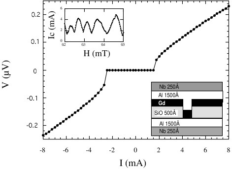
We study the specific junction Nb/Al/Gd/Al/Nb. The layers are prepared by e-beam evaporation in ultra-high-vacuum on a silicon substrate held at room temperature. Layer thicknesses are controlled during growth with a quartz crystal monitor. A typical rate of 1 Å/s is used for Gd. The base pressure is below Torr, and the working pressure is Torr for Gd, Torr for Al and Nb. The junction area ( mm2) is defined by evaporating insulating SiO through shadow masks at Torr typically. The inset of Fig. 1 shows a schematic cross section of the junction, which is made of two Nb leads of 250 Å, and a sandwich Al/Gd/Al with a Gd thickness ranging from 20 and 100 Å. A 1500 Å Al layer has been used to locally lower the superconducting of the junction and avoid spurious effects due to the Nb leads transitions.
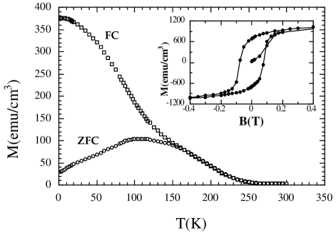
Several methods were used to characterize the Gd layer. First, Transmission Electron Microscopy images on Al/Gd reference samples evaporated under the same conditions as the junctions, have shown that Gd layers thinner than 20 Å are not continuous, thus imposing a lower bound on samples thicknesses. Gd is polycrystalline and the size of grains ranges between 70 to 100 Å. For the smaller thicknesses, the grains are elliptic, of typical dimension 20 Å 70 Å 70 Å. The magnetic properties of Gd were investigated by means of SQUID magnetometry. In Fig. 2, we show a Zero Field Cooled (ZFC) and Field Cooled (FC) magnetization curve in a low applied field (H=50 Oe). These curves exhibit a large thermomagnetic hysteresis with an irreversibility temperature () of 150 K, and a blocking temperature of about 120 K. We estimate that the Curie temperature range between 50 K and 100 K. This behavior is characteristic of a superparamagnet, in agreement with the granularity of the magnetic layer. From the saturation magnetization, the magnetic moment per atom is estimated to be , substantially below the Gd bulk moment of . We attribute this reduction of the saturation magnetization compared to the bulk value to frozen spins that do not align in the applied magnetic field due to spin glass effects as it is expected for Gd small grains [16, 17]. The coercitive field of the Gd layers is around 100 mT, for all the Gd thickness. The macroscopic magnetization of the granular Gd increases as the external field is increased because the giant spin grains align on average in the external field.
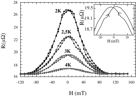
All the transport measurements have been performed with a highly sensitive dc-current method using a four probe technique [18]. Resistances range from a few m to a few and the voltage across the junction is of the order of a nanovolt. A typical current-voltage I-V characteristics is shown on Fig. 1. It displays a sizeable critical current Ic, whose amplitude strongly decreases with the Gd thickness, indicating a Josephson coupling between the superconducting electrodes through the ferromagnet. This will be exposed in details in a forthcoming publication. The modulation of Ic in a weak applied magnetic field (inset of Fig. 1) confirms the existence of a Josephson coupling and excludes that pinholes dominate the transport properties. In zero magnetic field (see Fig. 3) a first transition appears in transport measurements corresponding to the superconducting transition of Nb between 7.5 and 8 K, that induces superconductivity in Al by proximity. At lower temperatures the resistivity vanishes due to Josephson effect (inset of Fig. 3). Fig. 3 shows the effect of a magnetic field on the junction resistance, the magnetic field being applied along the layer and perpendicular to the current. The resistance is drastically reduced by the external magnetic field. We can exclude that this behavior originates from part of the bilayer Nb/Al becoming normal. The parallel critical field () in a thin film is , where is the penetration depth in the superconductor and the film thickness[19]. For Niobium this leads to T, a value much larger than the fields used in this investigation. As for Al, the magnetic field required to destroy superconducting proximity effect is larger than the bulk critical field 200 mT of Nb [20]. Therefore, the bilayer remains superconducting for a magnetic field up to 100 mT.
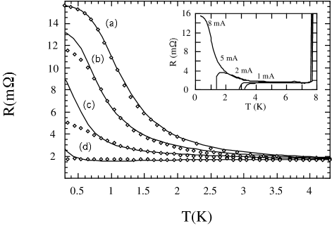
Fig. 4 shows the variations of the ohmic resistance at a fixed temperature as a function of the applied magnetic field. The sample is first zero field cooled from 10 K to the measurements temperatures. The magnetic field is swept from -150 mT up to 150 mT, and back to -150 mT. The crossover field for the negative magnetoresistance is independent on temperature, which is an additional proof that this effect does not originate from the destruction of superconductivity in the Nb/Al bilayer, in which case this crossover field would depend on temperature. Moreover, the hysteresis in the magnetoresistance clearly indicates the onset of a magnetic effect in the transport in the junction (inset of Fig. 4).
The de Jong-Beenakker theory cannot account for the present observations, since it would predict an increase of resistance upon spin polarization, and also because the relative change in resistance induced by a small spin polarization of 5-7 % would be of the order of the spin polarization [21], incompatible with the magnitude of the resistance variations shown on Fig. 3. We believe that the failure of the de Jong-Beenakker theory in our system lies in the fact that transport in the Gd grains is dominantly an out-of-equilibrium transport since the grains (70-100 Å) and the Gd thicknesses are small. We present here a modeling of this situation that qualitatively accounts for the negative magnetoresistance. In this model, the charge carriers are “hot” electrons, which wave vector and spin remain constant while they cross the grains. Given the small size of the grain, we neglect any inelastic scattering. The spin energy of an electron (hole) is , being the space-dependent exchange field. The relevant quantity for Andreev reflection is the exchange field at the grain boundary, a quantity which can be much smaller than the bulk value meV. The magnetism of Gd is very sensitive to growth parameters [22, 23], and surface magnetization can be strongly weakened by possible adsorbtion of oxygen atoms at the edge of Gd grains [24]. An applied magnetic field will favor ferromagnetism at the boundaries and increase . As the external field increases, the nucleation of boundary polarization is expected to favor the reversal of the bulk giant moment if the grain had a misoriented magnetization. This Gd grain modeling also allows to understand that the hysteresis in resistance is weaker than in magnetization, since the former involves boundary magnetism and the latter the superparamagnetic behavior of the giant spin grains.
Now, let us consider the semiclassical treatment of a N/FM/S junction [25], and assume a scattering only at the FM/S interface I2. The presence of a scattering at both interfaces leads to similar qualitative conclusions, as well as the S/FM/S junction, in which cases a numerical treatment is necessary and will be presented elsewhere[21]. We note the non-equilibrium distribution functions of right (left) movers with a spin at the I1=N/FM (I2=FM/S) interface. The Zeeman splitting in the FM region is taken into account by proper boundary conditions, e. g. at the I1 interface, being the equilibrium distribution function in the reservoirs. The exchange field and the superconducting gap are assumed to have step function variations at the interface I2. We have point split the two order parameters at this interface by assuming that electrons incoming from the S part will first experience the barrier potiential and next Zeeman splitting, or the opposite. In the first case, the barrier conductance is independent on spin polarization, whereas in the second situation, in which both orders coexist close to the interface, the I-V relation is
| (2) | |||||
with and are the Andreev and backscattered transmission coefficients [7]. The Landauer formula is
a quantity that increases with the spin polarization if [7]. As shown on Fig. 3, the best fits are in a qualitative agreement with experiments. Because of the mT hysteresis in conductance, the spontaneous boundary magnetization is expected to be finite. However we cannot resolve magnetic fields below mT whithin the present model.
Given the weakening of ferromagnetism at the grain boundaries [22, 23], we have shown that the observed negative magnetoresistance originates from an enhancement of Andreev reflection due to Zeemann splitting of “hot” carriers. This requires the coexistence of superconductivity and ferromagnetism close to the interface. A more complete understanding of this interface would involve a treatment of the influence of the ferromagnet onto the superconductor, and, in view of the reduction of magnetism, the possibility of cryptomagnetic [26], or cryptomagnetic-like structures [27] at the grain boundaries.
The authors thank M. Aprili, O. Buisson, P. Butaud, C. Chappert, H. Courtois, B. Douçot, M. Giroud, F. Hekking, T. Klapwijk, C. Lacroix, B. Lussier, K. Matho, B. Pannetier and Ned S. Wingreen for fruitful discussions and their encouragements, and M.O. Ruault for the TEM images.
REFERENCES
- [1] J. Jiang, D. Davidovic, D. Reich, and C. Chien, Phys. Rev. Lett. 74, 314 (1995).
- [2] T. Mühge et al., Phys. Rev. B 57, 5071 (1998).
- [3] V. Petrashov, V. Antonov, S. Maksimov, and R. Shaikhaidarov, JETP Lett 59, 551 (1994).
- [4] M. Lawrence and N. Giordano, J. Phys - Condens. Matter 8, L563 (1996).
- [5] M. Giroud et al., Phys. Rev. B 58, R11872 (1998).
- [6] A. Andreev, JETP 19, 1228 (1964).
- [7] G. Blonder, M. Tinkham, and T. Klapwijk, Phys. Rev. B 25, 4515 (1982).
- [8] M. de Jong and C. Beenakker, Phys. Rev. Lett. 74, 1657 (1995).
- [9] R. Soulen et al., Science 282, 85 (1998).
- [10] S. Upadhyay, A. P. R. Louie, and R. Buhrman, Phys. Rev. Lett. 81, 3247 (1998).
- [11] R. Meservey and P. Tedrow, Phys. Rep. 238, 173 (1994).
- [12] R. Meservey, D. Paparaskevopoulos, and P. Tedrow, Phys. Rev. B 22, 1331 (1980).
- [13] G. Busch, M. Campagna, P. Cotti, and H. Siegman, Phys. Rev. Lett. 22, 597 (1969).
- [14] T. Kasuya, (G.T. Rado and H. Suhl, 111 Fifth Avenue, New York 10003, 1966), Vol. IIB, p. 237.
- [15] B. Coqblin, The electronic structure of rare-earth metals and alloys : the magnetic heavy rare-earth (Academic Press, London, 1977).
- [16] D. Douglass, J. Bucher, and L. bloomfield, Phys. Rev. Lett. 68, 1774 (1992).
- [17] Y. Li, C. Polaczyk, J. Kapoor, and D. Riegel, J. Magn. Magn. Matter 165, 165 (1992).
- [18] P. Dauguet, P. Gandit, and J. Chaussy, J. Appl. Phys. 79, 5823 (1996).
- [19] M. Tinkham, Introduction to superconductivity (Mc Graw-Hill, New York, 1996).
- [20] J.-P. Hurault, Phys. Lett 20, 587 (1966).
- [21] R. Mélin and O. Bourgeois, in preparation.
- [22] M. Farle et al., Phys. Rev. B 47, 11571 (1993).
- [23] M. Gajdzik, T. Trappmann, C. Sürgers, and H. Löhneysen, Phys. Rev. B 57, 3525 (1998).
- [24] D. McIlroy et al., Phys. Rev. Lett. 76, 2802 (1996).
- [25] M. Octavio, M. Tinkham, G. Blonder, and T. Klapwijk, Phys. Rev. B 27, 6739 (1983).
- [26] P. Anderson and H. Suhl, Phys. Rev. 116, 898 (1959).
- [27] A. Buzdin and L. Bulaevskii, JETP 67, 576 (1988).