[
Size Effects in Carbon Nanotubes
Abstract
The inter-shell spacing of multi-walled carbon nanotubes was determined by analyzing the high resolution transmission electron microscopy images of these nanotubes. For the nanotubes that were studied, the inter-shell spacing is found to range from 0.34 to 0.39 nm, increasing with decreasing tube diameter. A model based on the results from real space image analysis is used to explain the variation in inter-shell spacings obtained from reciprocal space periodicity analysis. The increase in inter-shell spacing with decreased nanotube diameter is attributed to the high curvature, resulting in an increased repulsive force, associated with the decreased diameter of the nanotube shells.
pacs:
61.46.+w, 81.10.Bk]
The discovery of multi-walled carbon nanotubes [1] and single-walled carbon nanotubes [2, 3] has prompted numerous studies of the structure, properties [4, 5, 6, 7, 8], and potential applications [9, 10, 11] of these exotic materials. For example, nanotubes are expected to have a high strength-to-weight ratio [11], which is advantageous in advanced composites to be used in high performance materials such as aircraft frames. The small dimension of the tubes shows promise for use as a gas absorption medium [12, 13], a field emitter for use in flat-panel displays [14], and a nanoscale electronic device [15, 16, 17, 18]. Most of the anticipated properties and applications are based on theoretical calculations for idealized tube structures [19, 20, 21]. A precise knowledge of the structure of real nanotubes and the interactions between them is essential for a reliable prediction of the potential applications.
Structural studies of carbon nanotubes have relied heavily on X-ray diffraction [22], scanning tunneling microscopy [23], and, predominately, high resolution transmission electron microscopy (HRTEM) and electron diffraction [1, 24, 25, 26]. Carbon nanotubes are composed of concentric cylindrical graphene tubules, each with a structure similar to that of a rolled-up graphene sheet [4]. Iijima first showed with transmission electron microscopy that the inter-shell spacing of carbon nanotubes is about 0.34 nm [1], which was later confirmed by Zhang et. al with an electron diffraction study [24]. Saito et. al used powder X-ray diffraction to determine the lattice parameters of a bulk nanotube sample [22], and they concluded that the average inter-shell spacing is 0.344 nm. Bretz et. al, on the other hand, obtained a 0.375 nm spacing [27], and Sun et al. obtained a 0.36 nm spacing [28] by analyzing the HRTEM image of individual multi-walled nanotubes. These reports suggest a spread of inter-shell distances in carbon nanotubes, with a possible dependence on the tube size. In the present work, we study the HRTEM nanotube images for several different multi-walled carbon nanotubes in an effort to understand the previously-reported variation in the inter-shell spacing. To obtain quantitative results, we carried out a digital image analysis of HRTEM images, which allows us to relate the inter-shell spacings to the nanotube diameter and the number of shells in a given nanotube.
Carbon nanotube samples were prepared by the usual arc-discharge method [1, 6]. The core of the deposit was crushed and dispersed in ethanol. A drop of this solution was transferred to a holey carbon microscope grid. HRTEM images were obtained with a TOPCON 002B microscope at 200KV or a JEOL 4000 EX at 400KV accelerating voltage. The images were scanned with a CCD camera and stored in a 1024 1024 pixel array of 256 gray-scale levels.
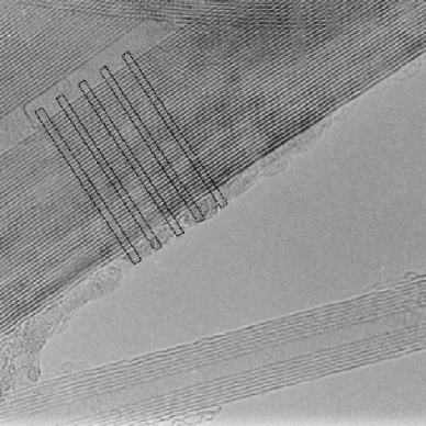
We carried out high resolution image analysis of nanotubes in real space, which allows us to measure individual inter-shell spacings as a function of tube diameter. Each data point is obtained as an average over 5 measurements to reduce the error to 3%, as shown in Fig. 1.
Our data for all tube diameters that were studied show that the inter-shell spacing () ranges from 0.34 to 0.39 nm, and that increases as the tube diameter decreases. The empirical equation for the best fit to the data is
| (1) |
where is the inner tube diameter, and all the constants are in nm. Equation (1) was obtained by a least square fit of the function to our experimental data (where , , and are adjustable parameters), as depicted by the solid curve in Fig. 2.

The inter-shell spacing decreases exponentially and approaches 0.344 nm as the tube diameter increases.
For small tube diameters ( 10 nm), an increase in the spacing with decreasing tube diameter is physically reasonable, since the repulsive forces of the graphene basal planes between adjacent tubes are larger for smaller diameter tubes, owing to their larger curvature, which perturbs the geometric and electronic structures relative to a planar graphene sheet. It has been pointed out that the HRTEM projected images of small diameter carbon naotubes is asymmetric [29], but this effect on the measured inter-shell spacing is small and is within our experimental error. From Eq. (1) we estimated that the spacing is 0.41 nm for a 0.7 nm diameter tube, the smallest diameter carbon nanotube observed experimentally [30]. Furthermore, for finite sized tubes, the allowed diameters are discrete, which poses constraints on the inter-shell spacings. We calculated the distribution of allowed tube diameters with different helicities according to Eq. (2)
| (2) |
where and are integers. A discontinuity of 0.01 nm occurs for very small diameter nanotubes ( 3 nm). This geometric effect may explain the deviation of values from the predicted curve shown in Fig. 2.
For large tube diameters ( 10 nm), the variation in spacing can be explained by assuming a uniform charge density
| (3) | |||||
| (4) |
where is the tube radius and is 0.344 nm, the asymptotic limit of the spacing.
The asymptotic limit deduced by Eq. (1) is 0.344 nm, the same spacing as that in a turbostratic graphite. This is expected since defect-free multi-walled nanotubes have circular cross-sections. In any single multi-walled nanotube, the diameter of each constituent graphene shell is different, which prevents perfectly correlated graphitic stacking. Some of the fluctuations in the spacings may be associated with the jumps in spacing at points where the helix angle changes [31]. A value smaller than that of a turbostratic graphite, however, may occur when the energy gained by the local graphitic stacking is less than the energy introduced by the defects associated with the stacking. Inter-shell spacings smaller than 0.344 nm, resulting from a polygonal cross-section, have frequently been observed for large diameter nanotubes [32, 33] and for vapor-grown carbon fibers [34].
We also measured the lattice constants in reciprocal space, which complement the results obtained from real space images. With a known minimum diameter of a nanotube (measured directly from the HRTEM images), we calculated the diffracted spot positions from a crystal with a slowly-varying unit cell length defined by Eq. (1). The calculated results were then compared to the experimental data. Figure 3a presents data for a nanotube with the 0.213 nm lattice fringes of the graphite basal plane clearly resolved, and the corresponding FFT is shown in Fig. 3b.
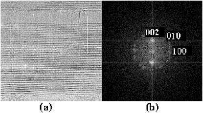
The inter-shell spacings () were deduced from the power spectra, using the location of the highest intensity as the spot position, as shown in Fig. 3b
We used the 0.213 nm spacing between {100} fringes as a calibration standard, based on the X-ray diffraction study [22] showing that the C-C bond lengths in the nanotubes are the same for both graphite and carbon nanotubes (0.142 nm) [22]. The tube diameters, defined as the average diameter () of the tubes used for the FFT, were obtained from the real space images.
In reciprocal space, the scattering amplitude is
| (5) |
where is the unit cell in the crystal, is the reciprocal lattice vector, is the atomic position in real space, and is proportional to the atomic form factor for electron scattering of carbon and is a slow varying function of for electron scattering. Since we were only interested in diffraction along the (002) direction, we constructed a crystal of parallel graphene sheets with varying inter-shell distances, as depicted in Fig. 4a.


Defining to be perpendicular to the graphene planes, we can express as a function of the cell (for )
| (6) |
where is the atomic position of the unit cell along the -axis relative to the origin, is evaluated with Eq. (1), and is the minimum radius of the nanotubes. The scattering amplitude for the crystal shown in Fig. 4a is
| (7) |
where is the total number of unit cells along the axis. Thus the diffracted intensity is
| (8) |
For a crystal with a constant , Eq. (8) can be evaluated analytically, and the peak position (defined as the intensity maximum of the peak) is at . For a crystal with a slowly varying for all tubes, the peak is shifted relative to the value for . Using this model, we evaluated numerically the spacing as a function of the average tube diameter (), starting with the smallest possible value which can occur for a given , where is the number of shells in a nanotube. By knowing the number of shells and the average diameter of a nanotube, we can predict the (002) spot position in Fourier space. The resulting curves for = 2, 5, 10, and 40 are shown in Fig. 4b. The data from the Fourier analysis of the three tubes surveyed in Fig. 2 (where = 6, 7, and 41) agree with our model, supporting our conclusion that the inter-shell spacing is a function of tube diameter.
We also found that the nanotubes with smaller innermost tube diameters often have fewer shells. This may be because that the kinetics of the growth reaction is correlated with the product stability. According to the multi-walled nanotube growth mechanism [7, 35], nanotubes grow by first forming a nucleating shell, followed by epitaxial growth of additional shells. Larger inter-shell spacings resulting from a higher strain energy of the nanotubes decreases the stability of the nanotube. Because of the larger inter-shell spacings and lower stability of small diameter tubules, the epitaxial growth of additional shells onto the nucleating core is slower for smaller diameter tubes in comparison with larger diameter tubes. Therefore, the radial growth rate of nanotubes is also expected to be related to the nucleating tube diameter.
The small number of shells may also contribute to the size effect that causes increased inter-shell spacing. This effect, however, is expected to be smaller compared to the diameter effect. According to the shell-by-shell growth model, a variation of the inter-shell spacing as a function of requires a change in the inter-shell spacing as the number of shells increases, which would result in a decrease in C-C bond length. For example, a spacing that changes from 0.37 to 0.35 nm will result in a 5% decrease in bond length, which implies reducing the C-C bond length from 0.142 nm to 0.134 nm, a nearly impossible process. Our experimental results can be explained solely by the diameter size effect, which suggests that the effect due to a small number of carbon shells is within the experimental uncertainties. Incorporation of the effect may, however, provide further refinement to our model.
In summary, we have studied the nanotube structures by high resolution transmission electron microscopy and digital image analysis. We found that the inter-shell spacing of nanotubes decreases with increasing tube diameter, approaching nm asymptotically at a tube diameter of roughly 10 nm. The size effect is more profound in the small diameter ( 10 nm) region, where each additional shell results in a measurably different spacing. The physical and chemical properties may also vary owing to the change in inter-shell spacing of the nanotubes. For example, nanotubes of larger inter-shell spacing should be less stable and, therefore more reactive. The variation in interaction forces of small diameter nanotubes should modify single-walled carbon nanotube surface properties, which may result in useful characteristics for storage media such as hydrogen fuel cells and batteries.
We thank Dr. S. Iijima for helpful discussions. CHK and PMA acknowledges the financial support from the UC Energy Institute and the Alexander von Humboldt Foundation, respectively. Part of the work by ME is supported by the Ministry of Education, Science and Culture, Japan. The work at MIT is supported by NSF grant DMR-95-10093.
REFERENCES
- [1] S. Iijima, Nature 354, 56 (1991).
- [2] S. Iijima and T. Ichihashi, Nature 363, 603 (1993).
- [3] D. S. Bethune et al., Nature 363, 605 (1993).
- [4] M. S. Dresselhaus, G. Dresselhaus, and R. Saito, Carbon 33, 883 (1995).
- [5] J. W. Mintmire and C. White, Carbon 33, 893 (1995).
- [6] T. W. Ebbesen and P. M. Ajayan, Nature 358, 220 (1992).
- [7] M. Endo and H. W. Kroto, J. Phys. Chem. 96, 6941 (1992).
- [8] N. G. Chopra et al., Nature 377, 135 (1995).
- [9] P. M. Ajayan and S. Iijima, Nature 361, 333 (1993).
- [10] A. G. Rinzler et al., Science 269, 1550 (1995).
- [11] R. S. Ruoff and D. C. Lorents, Carbon 33, 925 (1995).
- [12] M. W. Maddox and K. E. Gubbins, Langmuir 11, 3988 (1995).
- [13] A. C. Dillon et al., Nature 386, 377 (1997).
- [14] W. A. de Heer, A. Chtelain, and D. Ugarte, Science 270, 1179 (1995).
- [15] L. Chico et al., Phys. Rev. Lett. 76, 971 (1996).
- [16] M. Menon and D. Srivastava, Phys. Rev. Lett. 79, 4453 (1997).
- [17] T. W. Odom, J.-L. Huang, P. Kim, and C. M. Lieber, Nature 391, 62 (1998).
- [18] J. W. G. Wildoer et al., Nature 391, 59 (1998).
- [19] N. Hamada, S. Sawada, and A. Oshiyama, Phys. Rev. Lett. 68, 1579 (1992).
- [20] M. R. Pederson and J. Q. Broughton, Phys. Rev. Lett. 69, 2689 (1992).
- [21] K. Akagi et al., Phys. Rev. Lett. 74, 2307 (1995).
- [22] Y. Saito et al., Phys. Rev. B 48, 1907 (1993).
- [23] M. Ge and K. Sattler, Science 260, 515 (1993).
- [24] X. F. Zhang et al., J. Cryst. Growth 130, 368 (1993).
- [25] High-Resolution Transmission Electron Microscopy and Associated Techniques, edited by P. R. Buseck, J. M. Cowley, and L. Eyring (Oxford University Press, New York, 1988).
- [26] C.-H. Kiang et al., J. Phys. Chem. 98, 6612 (1994).
- [27] M. Bretz, B. G. Demczyk, and L. Zhang, J. Cryst. Growth 141, 304 (1994).
- [28] X. Sun et al., Phys. Rev. B 54, R12629 (1996).
- [29] J. M. Cowley and S. D. Packard, Ultramicroscopy 63, 39 (1996).
- [30] C.-H. Kiang and W. A. GoddardIII, Phys. Rev. Lett. 76, 2515 (1996).
- [31] M. Liu and J. M. Cowley, Carbon 32, 393 (1994).
- [32] M. Liu and J. M. Cowley, Ultramicroscopy 53, 333 (1994).
- [33] T. W. Ebbesen, Annu. Rev. Mater. Sci. 24, 235 (1994).
- [34] J. S. Speck, M. Endo, and M. S. Dresselhaus, J. Cryst. Growth 94, 834 (1989).
- [35] S. Iijima, P. M. Ajayan, and T. Ichihashi, Phys. Rev. Lett. 69, 3100 (1992).