Current responsivity of semiconductor superlattice THz-photon detectors
Abstract
The current responsivity of a semiconductor superlattice THz-photon detector is calculated using an equivalent circuit model which takes into account the finite matching efficiency between a detector antenna and the superlattice in the presence of parasitic losses. Calculations performed for currently available superlattice diodes show that both the magnitudes and the roll-off frequencies of the responsivity are strongly influenced by an excitation of hybrid plasma-Bloch oscillations which are found to be eigenmodes of the system in the THz-frequency band. The expected room temperature values of the responsivity ( 2–3 A/W in the 1–3 THz-frequency band) range up to several percents of the quantum efficiency of an ideal superconductor tunnel junction detector. Properly designed semiconductor superlattice detectors may thus demonstrate better room temperature THz-photon responsivity than conventional Schottky junction devices.
pacs:
73.20.Dx, 73.40.GkI INTRODUCTION
Theoretical investigations of high-frequency properties of semiconductor superlattices have been carried out for almost thirty years starting from the trail-blazing works by Esaki and Tsu[2, 3]. They proposed to prepare superlattices made of different semiconductor materials in order to realise an artificial periodical system that would allow to observe Bloch oscillations due to Bragg reflection of electrons from the boundaries of the Brillouin zone. Making use of the semiclassical Boltzmann equation they found that the dc current-voltage characteristics of the superlattice should show a negative differential conductance in sufficiently strong electric fields, namely, when the Bloch frequency (where is the electron’s charge, is the dc electric field in the superlattice, is the superlattice period, is the Plank’s constant) becomes comparable to the effective scattering frequency [2]. They proposed to make use of the negative differential conductance for development of an oscillator in the THz-frequency band[2] and also suggested that the superlattice might posses promising properties as an artificial material for non-linear mixing of photons[3].
Later, several papers have proposed[4, 5, 6] to probe Bloch oscillations in a superlattice in a strong dc electric field by applying an additional strong ac field. Self- induced transparency[4], dc current suppression by a strong ac field causing dynamical localisation of carriers [4, 5, 6, 7, 8, 9, 10, 11, 12, 13, 14, 15, 16], absolute negative conductance[4], and current harmonics generation with oscillating power-dependence[4, 6] have been predicted to occur in the presence of resonant interaction between Bloch oscillating electrons and a strong THz-frequency radiation.
A profound analogy between the dynamics of electron wave-packets in periodic systems and the dynamics of superconducting Josephson junctions[17, 18] was put forward to explain the main features of the superlattice THz- frequency response[18]. It has been suggested, in particular, that the resonant steps on the dc current- voltage characteristics of the irradiated superlattices[18] should occur in analogy with ‘Shapiro steps’ normally observable in irradiated superconducting junctions[19]. Several recent papers show that the curious behaviour of electrons in the superlattices may give rise to a rich variety of new non-linear phenomena occurring in the THz- field irradiated superlattices [20, 21, 22, 23, 24, 25]
In a number of papers Esaki-Tsu negative differential conductance was found to be experimentally realisable[26, 27] and has been carefully examined [28, 29, 30] in the context of development of new millimetre-wave band (0.03-0.3 THz) oscillators. On the other hand, the recent observations of a strong dc current suppression indicating dynamical localisation of electrons[31], absolute negative conductance[32, 33], and ‘Shapiro steps’ on the dc current-voltage curve of the THz-field irradiated superlattices[34] open the prospects for applications of the superlattices as novel solid state detectors operating in 1-10 THz-frequency band which the Bloch frequency in the superlattices normally belongs to[35].
It has recently been estimated[36] that the room temperature current responsivity of a superlattice detector ideally coupled to the THz-photons can nearly reach the quantum efficiency (where is the incident radiation frequency) in the limit of high frequencies . This value of the responsivity is being normally considered as a quantum limit for detectors based on superconducting tunnel junctions operating at low temperatures[19]. For high frequencies the mechanism of the THz-photons detection in superlattices was described[36] as a bulk superlattice effect caused by dynamical localisation of electrons.
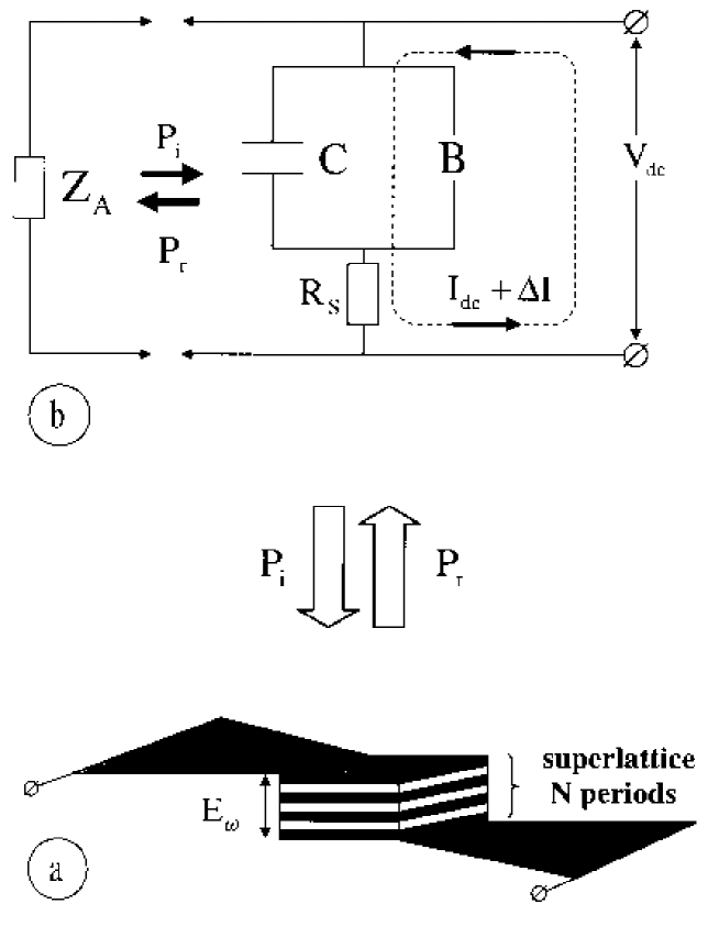
In the present paper we develop a self-consistent theory of the superlattice current responsivity. We apply the Boltzmann equation approach for describing the electron motion in the superlattice miniband[4] and assume an equivalent circuit for the superlattice coupled to a broad-band antenna (see Fig. 1), which is similar to the equivalent circuit used in resonant-tunnelling[37] and Schottky diodes[38] simulations. The suggested equivalent circuit of the device allows one to treat microscopically the high-frequency response of the miniband electrons and, simultaneously, take into account a finite matching efficiency between the detector antenna and the superlattice in the presence of parasitic losses. Our analytic results lead to the identification of an important physical concept: the excitation of hybrid plasma-Bloch[39] oscillations in the region of positive differential conductance of the superlattice. The numerical computations, performed for room temperature behaviour of currently available superlattice diodes, show that both the magnitudes and the roll-off frequencies of the responsivity are strongly influenced by this effect. The excitation of the plasma-Bloch oscillations gives rise to a resonant-like dependence of the responsivity on the incident radiation frequency, improving essentially the coupling of the superlattice to the detector antenna. We will also show that peak current densities in the device and its geometrical dimensions should be properly optimised in order to get maximum responsivity for each frequency of the incident photons. Finally, we will present numerical estimates of the responsivity for the 1-4 THz frequency band and compare its value with the quantum efficiency of an ideal detector.
II DESCRIPTION OF THE MODEL
For the description of the ac electron transport in a superlattice we use a quasi- classical wave packet treatment of the electron motion in a superlattice[2, 3, 4]. The energy spectrum of electrons in a miniband is taken in a tight-binding approximation:
| (1) |
where is the superlattice miniband width, is the superlattice period, is the quasi-momentum of an electron along the superlattice axis (perpendicular to the layers), are the quasi-momentum components along the superlattice layers, and is the effective mass of electrons along the superlattice layers.
The quasi-classical velocity of an electron moving along the superlattice axis and the time-derivative of the quasi-momentum are given by the expressions
| (2) | |||||
| (3) |
where is the electron charge, is the maximum velocity of electrons along the superlattice axis, and is the time-periodic electric field directed along the superlattice axis.
The electric current density is calculated from the distribution function,
| (4) |
which satisfies the time-dependent Boltzmann equation
| (5) |
Below we use the relaxation-time approximation for the collision integral[2, 3, 4]
| (6) |
where is the constant relaxation time for electron’s scattering, and is the equilibrium distribution function.
The relaxation-time approximation is, of course, an oversimplification of the numerous scattering processes taking place in a real superlattice. Nevertheless, several papers[40] have demonstrated that the phenomenon of dynamical localisation can be described very well within this approximation when compared to the corresponding results obtained from a full-scale Monte-Carlo simulation. This circumstance lends support to the simplified model for the collision integral. The great advantage of Eqs.(5) and (6) is that they allow an analytical calculation of the time-dependent current, to be used in the equivalent circuit analysis, and thus we can study in detail various parametric dependencies of the calculated quantities.
We would also like to emphasise here that the wave packet description of electron motion in a superlattice is valid if the following inequalities are fulfilled[4, 41]:
| (7) | |||||
| (8) | |||||
| (9) |
were is the width of the superlattice minigap, is the electron’s collision frequency, and is the characteristic frequency of the external ac field. We also assume that the electronic mean free path is smaller than the superlattice length in order to neglect the influence of the boundaries on the superlattice high- frequency properties.
III THEORETICAL FORMALISM
A Path integral
The exact solution of Eqs. (5) and (6) for arbitrary time-dependent electric field can be presented in the form of a path integral[42]:
| (10) |
Using Eqs.(4) and (10) we find the time-dependent current describing ac transport in a superlattice, with electron performing ballistic motion in a mini-band according to the acceleration theorem and suffering scattering[3, 4]:
| (11) |
where is the voltage across the superlattice perpendicular to the layers, is the superlattice length, is the number of periods in the superlattice sample, , is the area of the superlattice, is the superlattice mesa radius, and
| (12) |
is the characteristic current density. The integration over in Eq.(12) must be carried out over the Brillouin zone .
In particular, for a dc voltage applied to the superlattice (Eq.11) results in the Esaki-Tsu[2] current- voltage curve
| (13) |
At peak voltage or, equivalently, at peak electric field , the current in the superlattice reaches its maximum (peak) value , so that can be defined as the peak current density.
The peak current density and the scattering frequency can be considered as the main parameters of the employed model. They can readily be estimated from experimentally measured or numerically simulated values of and . For both degenerate and non-degenerate electron gas one gets [3, 4]
| (14) |
if , where is the equilibrium thermal excitation energy, is the Fermi energy of degenerate electrons, is the charge carrier density, is the density of states effective mass near the miniband bottom, and is the effective mass of electrons along the superlattice axis. In the particular case of the Boltzmann equilibrium distribution function Eq.(12) yields[4] , where are the modified Bessel functions.
B Monochromatic excitation
We now suppose that in addition to the dc voltage , an alternating sinusoidal voltage with a complex amplitude is applied to the superlattice:
| (15) |
Generally, can be found from an analysis of the equivalent circuit given in Fig. 1. We write the ac voltage amplitude as ; both and can be obtained self-consistently taking account of reflection of the THz photons from the superlattice and their absorption in the series resistor .
Making use Eq.(11) we obtain[4]:
| (16) |
where
| (17) |
According to Eq.(16), electrons in a superlattice miniband perform damped Bloch oscillations with the frequency , and the phase modulated by the external ac voltage.
In the limit of Eq.(16) reduces to the dc current-voltage curve given by Eq.(13). On the other hand, when the frequency of the ac voltage is small, , we get
| (18) |
which corresponds to a slow modulation of the Bloch frequency by external voltage. In this case the current in the superlattice follows instantaneously the time- dependent ac voltage according to the dc current-voltage curve.
Equation (16) contains, as special cases the following results: (i) a harmonic voltage () leads to dynamical localisation, and current harmonics generation with oscillating power dependence[4]; (ii) a dc current- voltage characteristics of the irradiated superlattice shows resonance features (‘Shapiro steps’) leading to absolute negative conductance[4, 6, 18]; (iii) and to generation of dc voltages (per one superlattice period) that are multiples of [14].
C Method of perturbations
Let us assume that the external ac voltage is so small that perturbation theory holds, while the dc voltage applied to the superlattice keeps its finite value. Expanding Eq. (16) around at in a Taylor series, we obtain the time-dependent electric current in the form:
| (19) |
where
| (20) |
is the superlattice ac conductance[4], is the superlattice conductance at ,
| (21) |
is a dimensionless function describing the dependence of the superlattice conductance both on frequency and applied dc voltage (field), and
| (22) |
where
| (23) | |||||
| (24) |
is the change in the dc current in a superlattice caused by THz-photons[4].
At Eq.(20) yields the dc differential conductance of the superlattice
| (25) | |||||
| (26) |
while at one gets the well known Drude formula for the ac conductivity of the electron gas
| (27) |
where the small-field dc conductivity of the superlattice can be given in terms of the dc conductance or, equivalently, in terms of peak current density and the peak electric field
| (28) |
According to Eqs.(15) and (19) the ac power absorbed in the superlattice is
| (29) |
where the real part of the superlattice conductance can be presented in analogy with Eq. (23) in a finite difference form[4, 43]
| (30) | |||||
| (31) |
We note here that our calculations assume a uniform dc/ac electric fields inside the superlattice. This assumption is justified for the sub-threshold dc electric fields , and/or for ac field frequencies larger than the transit-time frequency of space-charge waves in the superlattice[39].
D Stimulated emission and positive photo-current
Equation (31) for the superlattice conductance demonstrates a possibility of the resonant interaction of the THz-photons with electrons performing damped Bloch oscillations in the superlattice. For the condition for the resonance has a form which can be equivalently expressed as . At dc electric fields the real part of the superlattice conductance starts to be negative which corresponds to negative absorption (stimulated emission) of the THz-photons. In the limit photons with frequency are absorbed and the ones having frequency are emitted.
Equation (22) describes the dc current change in the superlattice under the influence of the THz-photons. The standard result of the classical rectification theory[19]
| (32) |
where
| (33) |
is the second derivative of the dc current-voltage curve of the superlattice, is obtained from Eq. (22) when the electron system relaxes during one period of the ac field.
At dc bias fields the current change in the irradiated superlattice is negative which corresponds to the onset of suppression of the current due to dynamical localisation of carriers [4, 5, 6, 7, 8, 9, 10, 11, 12, 13, 14, 15, 16]. In the opposite case a positive current change (positive photocurrent) occurs. It is important to note that the condition of occurrence of the positive photo-current implies, according to Eqs.(22) and (29), the existence of stimulated emission of photons from the superlattice, .
The increase of the dc current in superlattices caused by stimulated emission of THz-photons has recently been observed in experiments[34]. These experimental results lend support to the validity of the theoretical formalism employed in the present paper for the analysis of the superlattice THz-field response.
IV CURRENT RESPONSIVITY
A Equivalent circuit calculation
We define the current responsivity[19] of the superlattice detector as the current change induced in the external dc circuit per incoming ac signal power .
| (34) |
This definition takes into account both the parasitic losses in the detector and the finite efficiency for impedance-matching of the incoming signal into the superlattice diode. In the further analysis of the current responsivity we use both the frequency and the angular frequency notations.
According to Eqs.22 and 29, in the small-signal approximation both the dc current change and the power absorbed in the superlattice are proportional to the square modulus of the complex voltage . This circumstance permits us to calculate self-consistently for given values of the incoming power making use a linear ac equivalent circuit analysis and, then, find the current responsivity .
The results of the calculation of the superlattice current responsivity are presented in the following form:
| (35) |
where
| (36) |
is the superlattice current responsivity under conditions of a perfect matching and neglecting parasitic losses ()[36] ,where is the series resistance.
The factor in Eq. (35) describes the effect of the electrodynamical mismatch between the antenna and the superlattice and the signal absorption in the series resistance
| (37) |
The first factor in Eq. (37) describes the reflection of the THz-photons due to mismatch of the antenna impedance and the total impedance of the device , with the second one being responsible for sharing of the absorbed power between the active part of the device described by the impedance and the series resistance .
The superlattice impedance is defined as
| (38) |
where is the superlattice conductance, is the capacitance of the superlattice, and is the average dielectric lattice constant.
Finally, the last factor in Eq. (35) describes the redistribution of the external bias voltage between the dc differential resistance of the superlattice and the series resistance , with the dc voltage drop on the superlattice being determined by the solution of the well-known load equation[19]
| (39) |
B Classical rectification at high frequencies
Suppose now that the following set of inequalities is satisfied
| (40) | |||||
| (41) | |||||
| (42) |
which implies that the frequency of the incident radiation is small in comparison with the scattering frequency of electrons , series resistance is small in comparison with the small-field dc resistance of the superlattice and the appropriate time of the device is high enough. In this case Eq. (35) gives
| (43) |
Equation (43) was obtained by Sollner et.al.[37] following Torrey’s and Whitmer’s approach[38] developed for analyses of classical crystal rectifiers. They also took account of the mismatch between the antenna impedance and the device impedance. It was applied to analyse detection of photons by resonant tunnelling diodes in the THz- frequency range. This expression demonstrates that the responsivity of the classical rectifier at high frequencies is proportional to the second derivative of the dc current-voltage curve, and hence strongly decreases with increasing of frequency, .
The factor in Eq. (43) defines the roll-off frequency for the current responsivity and, consequently, capacitance of the device should be minimised in order to increase the responsivity in the high frequency range. The fast decrease of the responsivity with increasing of frequency can be attributed to imperfect matching of the device to the antenna impedance when incoming photons either are reflected from the device or are absorbed in the series resistor.
In our case Eq. (43) shows that the current responsivity of the superlattice can reach its maximum (negative) value at bias voltage , i.e. in the region of the positive conductance. Further, the responsivity of the superlattice does not depend on the length of the device because and , and, finally, the responsivity is proportional to the current density . Consequently, in order to increase the responsivity in the high-frequency range one should employ highly conductive superlattice samples for which inequalities (37)-(39) may be not satisfied. In this case the interaction of the superlattice with the incoming radiation can be essentially changed by excitation of the eigenmodes in the superlattice device.
C Superlattice dielectric function. Hybridisation of Bloch and plasma oscillations
Let us analyse the condition of optimised matching of the superlattice to the incident radiation going back to the general Eq. (35). Assuming the limit of negligible series resistance this condition can be obtained from solution of the equation
| (44) |
for the complex frequency . This solution determines the resonant line position and the line width at which the absorption in the superlattice tends to its maximum value.
Using Eqs. (20) and (38) one can transform Eq. (44) to the following form:
| (45) |
where
| (46) |
is the dielectric function of the superlattice, with the dc field being applied to the device[39], is defined by Eq. (21).
In the high-frequency limit the solution of Eq. (44) coincides with the solution of the equation
| (47) |
describing eigenfrequencies of the hybrid plasma-Bloch oscillations in a superlattice[39]
| (48) |
where is the plasma frequency of electrons in a superlattice. The plasma frequency can be given in terms of the small-field dc conductivity or, equivalently, in terms of the peak current density
| (49) |
Equation (49) reduces in the particular case of wide-miniband superlattices () to the standard formula .
In the limiting case of small applied dc electric fields one finds from Eq. (48) the plasma frequency , while in the opposite case , the Bloch frequency is recovered. The scattering frequency in Eq. (48) is responsible for the line width of the plasma-Bloch resonance.
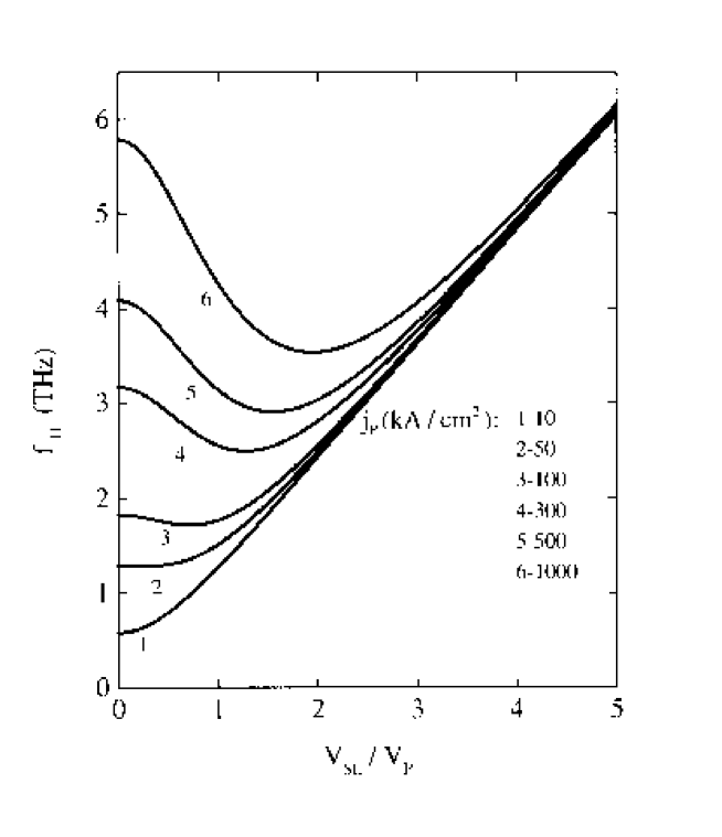
We have calculated the hybrid plasma-Bloch oscillation frequency , using Eqs. (48) and (49), for the typical values of the superlattice parameters[28, 29, 30] , Å, kV/cm, THz for different values of the current densities (Fig. 2). For small values of the current densities kA/cm2 the frequency of the hybrid oscillation increases with applied voltage in all range of the parameter . On the other hand, for higher values of the current densities kA/cm2 the hybrid oscillation’s frequency starts to decrease with increasing bias voltage in the sub-threshold voltage range . Then, at super-threshold voltages , starts to increase again tending to the Bloch frequency. It is important to note that at high values of the dc current densities the hybrid plasma-Bloch oscillations become well defined eigenmodes of the system (). Therefore, an essential improvement of the matching efficiency between antenna and the superlattice can be expected in the high- frequency range due to a resonant excitation of this eigenmode in the device.
D High-frequency limit
In the high-frequency case, when the signal frequency is larger than the scattering frequency , description of the superlattice response based on the classical rectification theory is no longer valid. Let us employ here Eq. (36) in order to analyse the high-frequency limit of the responsivity in the ideal case of the perfect matching and neglecting the series resistance. At , i.e. in the frequency band were ac field absorption and negative photo-current are predominated in the superlattice response, Eq. (36) yields the frequency- independent value for the current responsivity
| (50) |
At positive bias the responsivity is negative (reduction of the dc current occurs due to dynamical localisation of carriers [4, 5, 6, 7, 8, 9, 10, 11, 12, 13, 14, 15, 16]). The dc voltage dependence of the responsivity reproduces the dc Esaki-Tsu current-voltage curve[2]. The responsivity reaches its maximum value at . For high values of the applied voltages we get .
Let us compare the high-frequency limit of the responsivity of the superlattice with the quantum efficiency which is believed to be a fundamental restriction for the responsivity of superconductor tunnel junctions[19]. This quantum efficiency (or quantum limit) corresponds to the tunnelling of one electron across the junction for each signal photon absorbed[19], with a positive sign of the responsivity.
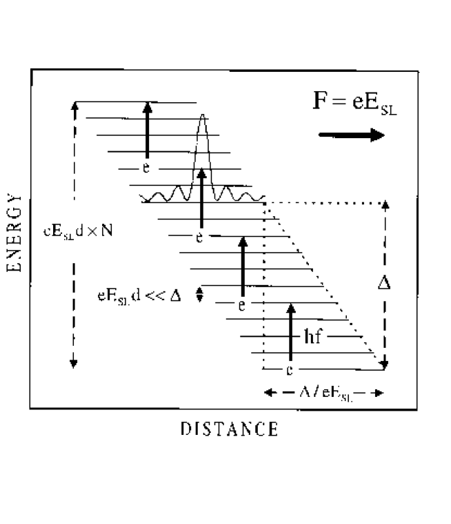
In our case the mechanism of the photon detection is different (see Fig. 3). Electrons move against the applied dc electric force due to absorption of photons. At the responsivity is negative, indicating that one electron is subtracted from the dc current flowing through the superlattice when the energy is absorbed from the external ac field. One half of this energy is needed for the electron to overcome the potential barrier which is formed by the dc force, with another half being delivered to the lattice due to energy dissipation. If the applied dc voltage is strong enough, i.e. , dissipation plays no essential role in the superlattice responsivity. In this case the energy should be absorbed from the ac field in order to subtract one electron from the dc current simply due to the energy conservation law.
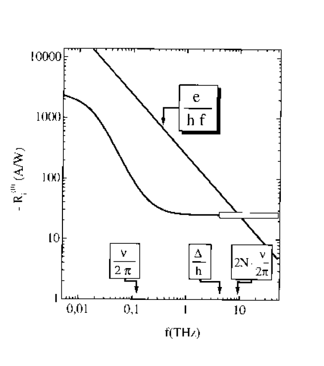
In order to demonstrate typical frequency scales involved in the problem we plot in Fig. 4 the frequency dependence of the responsivity for a superlattice with Å, , m, kV/cm, meV, THz at sub-threshold voltage as a function of the frequency . This example roughly corresponds to the superlattice samples experimentally investigated in Ref. [34]. The responsivity decreases in the region and, then, tends to the constant value determined by Eq. (50). At frequency the value of the responsivity equals the quantum efficiency .
However, the semiclassical approach employed in the present paper is restricted by the inequality . This inequality simply requires that there must be an allowed transition between different Wannier-Stark states in the superlattice miniband due to photon absorption as illustrated in Fig. 3. It is important to note that (where is the electron’s mean free path) in our calculations and, therefore, the current responsivity of the whole sample is always less than the quantum efficiency . In a wide-miniband superlattice with (or, equivalently, in a short superlattice sample with ) the responsivity is approaching the quantum efficiency in the high-frequency limit.
As was mentioned above, an increase of the length of a detector may have an advantage in the reduction of the parasitic capacitance , and, hence, in the increasing of the roll-off frequency of the device. It is interesting to note that in case of superconductor tunnel junctions connected in series the resulting responsivity is expected to be , implying that one photon should have been absorbed in each junction in order to add one electron to the dc circuit[19]. In the case of a superlattice samples consisting of unit cells (periods) the resulting responsivity can be presented as . For the responsivity of the unit superlattice cell starts to be larger than the quantum efficiency . This conclusion can be readily understood if one realises that due to absorption of one photon in the miniband electrons can ‘jump’ over several superlattice periods as illustrated in Fig. 3.
V RESULTS AND DISCUSSION
In this section we shall investigate the current responsivity of the superlattice making use of the Eq.(35) which takes into account both the finite matching efficiency between the antenna and the superlattice and the parasitic losses in the superlattice diode. We present our results using the dimensional value of (given in units of Ampere / Watt) and also introducing the normalised responsivity
| (51) |
which permits us to compare directly the responsivity of the superlattice with the quantum efficiency . In our calculations we use the typical geometrical dimensions of the superlattice samples investigated in the experiments[44, 45, 46] and also assume that the bow-tie antenna impedance does not depend on THz-photon frequency[34].
A Excitation of the plasma-Bloch oscillations
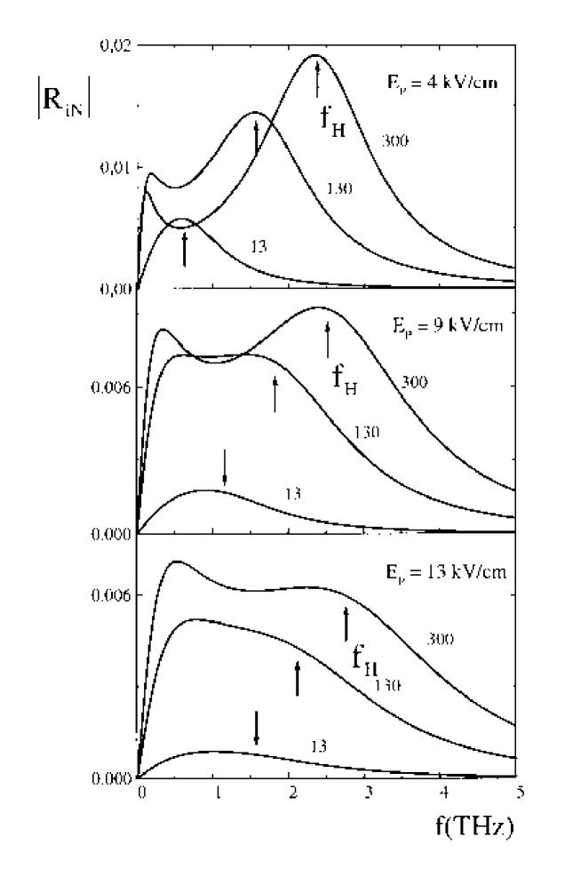
For demonstration of the frequency dependence of the superlattice current responsivity in the THz-frequency band we will focus on the GaAs/Ga0.5Al0.5As superlattices specially designed to operate as millimetre wave oscillators at room temperature. In Ref. [44] wide-miniband superlattice samples with Å, meV, , were investigated experimentally. They demonstrated a well-pronounced Esaki- Tsu negative differential conductance for kV/cm with the high peak current of the order of kA/cm2. The measured value of the peak current is in a good agreement with the estimate kA/cm2 for , K based on Eq. (12), if one assumes an equilibrium Boltzmann distribution for the charge carriers. From the peak electric field and current we find the scattering and plasma frequencies THz, THz, respectively, assuming for the average dielectric lattice constant. The maximum frequency for the semiclassical approach to be valid for these samples is THz. Figure 5 shows the frequency dependence of the normalised current responsivity calculated for three values of the peak current density in the superlattice, i.e. 13, 130, and 300 kA/cm2 and for three values of the peak electric field, 4, 9, and 13 kV/cm. We also use the typical values for the superlattice length m (superlattice consists of 100 periods), and assume m for the superlattice mesa radius[44, 45, 46]. We choose for the series resistance of the device in the THz- frequency band, i.e. the same value as for resonant tunnelling diodes having the same radius of mesas[37]. The calculations are performed in the region of the positive differential conductance for dc bias voltage close to the peak voltage ()
For kV/cm ( THz) Fig. 5 demonstrates well-pronounced resonant behaviour of the normalised responsivity as a function of frequency. The resonance frequency and the maximum value of the responsivity rise if the peak current density increases. For kA/cm2 the normalised responsivity reaches its maximum value ( A/W) at frequency THz . For higher values of the peak electric fields kV/cm ( THz) and kV/cm ( THz) the resonance line-widths are broadened due to implicit increase of the scattering frequencies. In particular, for kV/cm, kA/cm2 the normalised responsivity has an almost constant value ( A/W) up to THz and, then, rapidly decreases.
The frequency behaviour of the normalised responsivity originates from excitation of the plasma- Bloch oscillations in the superlattice. We indicate in Fig. 5 the positions of the hybrid frequencies with arrows. For small peak electric fields (low values of the scattering frequencies) the hybrid frequency corresponds to the maximum of the normalised responsivity. For higher values of the peak field (higher values of the scattering frequencies) it corresponds to the roll-off frequency at which the responsivity starts to decline.
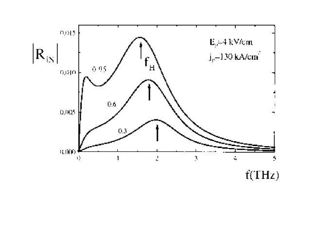
Frequency dependence of the responsivity for different applied dc fields , , 0.6 and 0.95 is illustrated in Fig. 6 for kA/cm2. The same geometrical dimensions and circuit parameters of the superlattice device have been chosen for calculations as previously. The normalised responsivity decreases with decreasing of the bias field tending to zero at . On the other hand, the position of maximum responsivity shifts to lower values with increasing of the bias field in full agreement with Eq.(48).
B Optimised superlattice length
The enhancement of the normalised responsivity requires an optimum matching efficiency of the superlattice to the broad-band antenna and minimisation of the parasitic losses in the series resistor. These requirements impose an optimum length of the superlattice for each chosen frequency of the incoming THz-photons and series resistance.
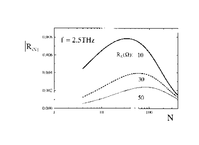
We show in Fig. 7 the dependence of the normalised responsivity on the number of the superlattice periods for THz.We used for calculation m, kA/cm2, , and three values of the series resistance , 30 and 50 . For all three values of the series resistance the responsivity displays a well pronounced maximum for the optimum number of the superlattice periods . The value of increases with increasing of the series resistance ( for , for and for for ). This result can be readily understood by recalling that a larger volume of the superlattice minimises parasitic losses for higher values of the series resistance because of reduction of the sample’s capacitance.
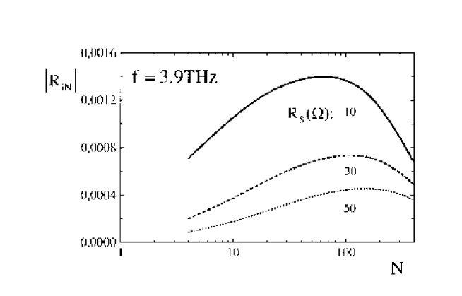
For incoming photon higher frequencies the parasitic losses in the superlattice device play even more important role leading to a further increase of . Figure 8 shows the dependence of the normalised responsivity on the number of the superlattice periods for THz and the same superlattice parameters as in Fig. 7. In this case ( for , for and for ). We can conclude, therefore, that the bulk mechanism of the superlattice high-frequency response provides important benefits for operation of the superlattice detectors in the THz-frequency band.
C Responsivity dependence on bias voltage
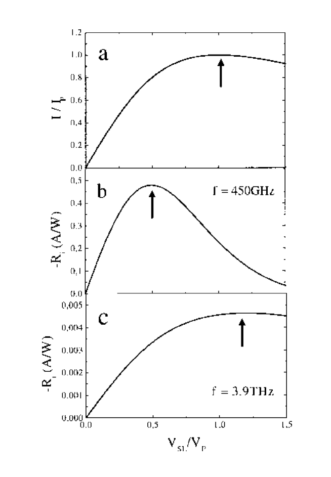
Experimental studies of interaction of high-frequency fields with the miniband electrons in semiconductor superlattices having a relatively small ( kA/cm2) current densities were performed[45, 46] for frequencies GHz, GHz and THz. A field-induced reduction of the current through the superlattice was reported, with a different bias dependence below and above a characteristic frequency (1THz). Distinct bias dependence of the responsivity was attributed to quasistatic () and dynamic () interaction of the miniband electrons with ac fields at frequencies below and above 1THz, respectively. The intraminiband relaxation time ( s) was estimated from experimental data[46].
In Fig. 9 we plot the dc bias dependence of the responsivity at GHz and THz for the superlattice parameters corresponding to experiments[46] ( kA/cm2, kV/cm, m, m, ) together with the dc Esaki-Tsu current-voltage curve. In a full agreement with the observations[46], at GHz responsivity reaches its maximum value at (roughly corresponding to the position of the maximum of the second derivative of the dc current-voltage curve), while for 3.9 THz-radiation the position of the maximum is shifted to the peak voltage . This can be readily understood if one takes into account that for the model of the classical rectification is no longer valid. In this case the current change under THz-photon irradiation is described by Eq. (22) giving the second derivative of the current in the finite difference form taking account of finite photon energies . At high frequencies this equation yields , i.e. the bias-field dependence of the responsivity should reproduce the dc current-voltage curve showing the maximum value at .
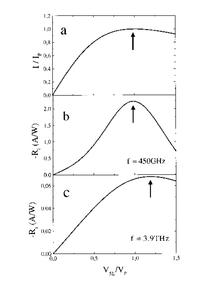
It is important to note that with increasing peak current densities this behaviour qualitatively changes. Figure 10 demonstrates the bias-field dependence of the responsivity for the same frequencies and superlattice parameters as Fig. 9 and for kA/cm2. First, we emphasise that the responsivity is considerably higher than in the previous case both for 450 and 3.9THz radiation. Second, for 450 GHz-radiation the responsivity reaches its maximum value at and not at as previously. For the high peak current densities the superlattice impedance variation due to applied dc voltage essentially changes the coupling efficiency between antenna and superlattice. This leads to a qualitatively different behaviour of the responsivity for low and high peak current densities: the latter can manifest in experiments a more efficient coupling of radiation into the superlattice.
D Optimised peak current density
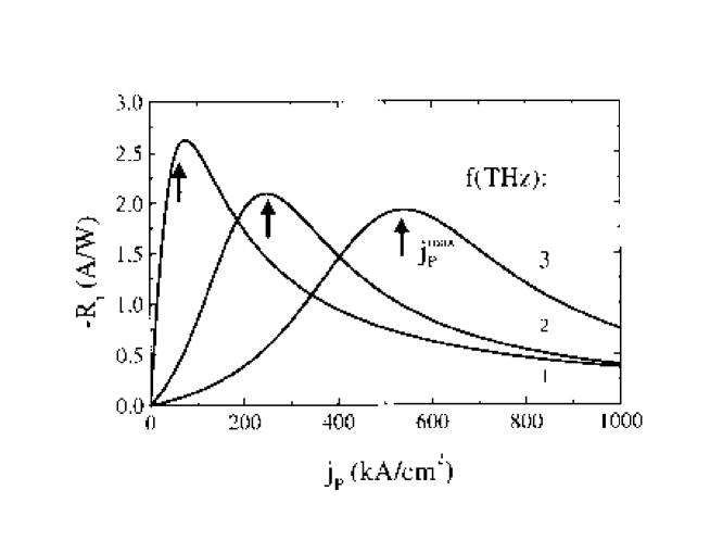
For a given superlattice geometry the current responsivity of the superlattice can also be enhanced by choosing an optimum value of the peak current densities. This circumstance is illustrated in Fig. 11 where we plot the responsivity as a function of the peak current density for , kV/cm, m, m, and for three frequencies of radiation, i.e. and 3 THz. For different frequencies the responsivity reaches its peaks at different values of which increases with increasing of the radiation frequency.
This behaviour can also be explained by excitation of the plasma-Bloch oscillations in the superlattice by THz- photons if one takes into account the resonant condition , where the hybrid frequency is given by Eq. (48) (see also Fig. 2). Calculated values THzkA/cm2, THzkA/cm2 and THzkA/cm2 are shown in Fig. 11 by arrows. They are in a good agreement with the positions of the peaks found from calculations based on the general Eq. (35).
We can conclude, therefore, that high current density superlattices should be used in order to achieve the large responsivity values (2-3 A/W) in the 1-3 THz -frequency band. The high current densities can be obtained by choosing wide-miniband and/or highly-doped samples. For example, according to Eq. (14) in superlattices with 130 meV[26] the peak current density 1000 kA/cm2 can be reached for cm-3. In this case the equilibrium thermal excitation energy ( 26 meV) and the Fermi energy of degenerate electrons ( 27 meV) are considerably smaller than the miniband width. Hence, Eq. (14) can be employed for the peak current density estimates both for room and low-temperature conditions.
Finally we would like to note that the measurements of the responsivity of resonant-tunnelling (double- barrier) heterostructure diodes reported in Ref. [[37]] were carried out at frequencies as high as 2.5 THz. The reported value of the responsivity was of the order of several A/W. As has been mentioned[37], this value is smaller by over an order of magnitude than the responsivity of THz-frequency Schottky diodes in this frequency band. We believe that an optimised superlattice detector as discussed above may have some advantages over these devices due to rather high expected current responsivity in the THz-frequency band.
VI CONCLUSIONS
In conclusion, we have calculated the current responsivity of a semiconductor superlattice detector in the THz-frequency band based on equivalent circuit modelling. Using a path integral solution of the Boltzmann equation within the relaxation-time approximation for the collision integral we have obtained an analytical expression for the responsivity, taking account of (i) frequency dependent superlattice response to a THz field caused by dynamical localisation of electrons, (ii) a finite matching efficiency between a detector antenna and the superlattice, and (iii) the presence of parasitic losses in the device caused by a series (contact) resistance.
We find that the responsivity of the superlattice ideally coupled to the incident radiation tends to a finite value with increasing radiation frequency. This value is simply determined by the energy conservation law governing the THz-photons absorption in the presence of scattering processes.
Excitation of plasma-Bloch oscillations in the superlattice (which are found to represent eigenmodes of the system in the THz-frequency band) can essentially enhance both the magnitude and the roll-off frequencies of the responsivity due to resonant coupling of radiation into the superlattice. The excitation of the plasma-Bloch oscillations can manifest itself as a resonance-like dependence of the normalised responsivity on the THz- photon frequency and (or) as a specific dependence of the responsivity on bias fields for superlattices showing high peak current densities.
Changes in peak current density and in superlattice length can effect drastically the coupling efficiency and parasitic losses in the superlattice device. These parameters are found to play an important role in the THz- field detector performance and need to be optimised for each value of the radiation frequency and series resistance. For higher frequencies the optimum length of the superlattice detector tends to increase demonstrating a benefit of a bulk-type mechanism of the THz-photon detection.
In currently available superlattices possessing the optimised length and the peak current the responsivity is expected to be as high as (2-3) A/W in the 1-3 THz-frequency band. These values of the responsivity range up to several percents of the quantum efficiency of an ideal superconductor tunnel junction for this frequency range. The analysis of the current responsivity performed in the present paper does not necessarily assume cooling of the superlattice: the estimated values of the current responsivity of superlattices can be expected at even room temperature.
Acknowledgements.
We would like to acknowledge fruitful discussions with K. F. Renk, S. J. Allen, N. J. M. Horing, A. Wacker, E. Schomburg, J. Grenzer, S. Winnerl, E. P. Dodin, A. Zharov, and D. G. Pavel’ev. A. A. I. gratefully acknowledges a guest professorship financed through the NATO Science Fellowship Programme.REFERENCES
- [1] Permanent address: Institute for Physics of Microstructures, Russian Academy of Science, 603600 Nizhny Novgorod, Russia.
- [2] L. Esaki and R. Tsu, IBM J. Res. Dev. 14, 61 (1970).
- [3] R. Tsu and L. Esaki, Appl. Phys. Lett. 19, 246 (1971).
- [4] A. A. Ignatov and Yu. A. Romanov, Sov. Phys. Solid State 17, 2216 (1975); Phys. Status Solidi B 73, 327 (1976).
- [5] V. V. Pavlovich and E. M. Epstein, Sov. Phys. Semicond. 10, 1196 (1976).
- [6] A. A. Ignatov and Yu. A. Romanov, Radiophysics and Quantum Electronics (Consultants Bureau, N.Y., 1978) Vol. 21, p. 90.
- [7] D. H. Dunlap and V. M. Kenkre, Phys. Lett. A 127, 438 (1988); Phys. Rev. B 37, 6622 (1987).
- [8] M. Holthaus, Phys. Rev. Lett. 69, 351 (1992).
- [9] D. H. Dunlap, V. Kovanis, R. V. Duncan, and J. Simmons, Phys. Rev. B 48, 7975 (1993).
- [10] X.-G. Zhao, X.-W. Zhang, S.-G. Chen, and W.-X. Zhang, Intern. Journ. of Mod. Phys. B 7, 4215 (1993).
- [11] M. Wagner, Phys. Rev. B 49, 16544 (1994).
- [12] X.-G. Zhao, R. Jahnke, Q. Niu, Phys. Lett. A 202, 297 (1995).
- [13] J. Rotvig, A. P. Jauho, and H. Smith, Phys. Rev. Lett. 74, 1831 (1995).
- [14] A. A. Ignatov, E. Schomburg, J. Grenzer, K. F. Renk, and E. P. Dodin, Z. Phys. B 98, 187 (1995).
- [15] J. Iñarrea and G. Platero, Europhys. Lett. 34, 43 (1996).
- [16] K. Johnsen, and A.P. Jauho, Phys. Rev. B 57, 8860 (1998).
- [17] M. B ütiker, Phys. Lett. A 96, 365 (1983).
- [18] A. A. Ignatov, K. F. Renk, and E. P. Dodin, Phys. Rev. Lett. 70, 1996 (1993); J. B. Xia, Phys. Rev. B 58, 3565 (1998).
- [19] For a review, see J. R. Tucker and M. J. Feldman, Rev. Mod. Phys. 57, 1055 (1985).
- [20] X. L. Lei, N. J. M. Horing, H. L. Cui, and K. K. Thornber, Appl. Phys. Lett. 65, 2984 (1994); Z. Phys. B 104, 221 (1997).
- [21] A. N. Korotkov, D. V. Averin, and K. K. Liharev, Phys. Rev. B 49, 7548 (1994).
- [22] O. A. Tkachenko, D. G. Baksheyev, and V. A. Tkachenko, J. Appl. Phys. 81, 1771 (1997).
- [23] X. L. Lei, J. Appl. Phys. 82, 718 (1997).
- [24] A. W. Ghosh, A. V. Kuznetsov, and J. W. Wilkins, Phys. Rev. Lett. 79, 3494 (1997).
- [25] K. N. Alekseev, E. H. Cannon, J. C. McKinney, F. V. Kusmartsev, and D. K. Cambell, Phys. Rev. Lett. 80, 2669 (1998).
- [26] A. Sibille, J. F. Palmier, H. Wang, and F. Mollot, Phys. Rev. Lett. 64, 52 (1990).
- [27] H. T. Grahn, K. von Klitzing, K. Ploog, and G. H. D öler, Phys. Rev. B 43, 12094 (1991).
- [28] M. Hadjazi, J. F. Palmier, A. Sibille, H. Wang, E. Paris and F. Mollot, Electronics Lett. 29, 648 (1993).
- [29] E. Schomburg, K. Hofbeck, J. Grenser, T. Blomeier, A. A. Ignatov, K.F. Renk, D.G. Pavel’ev, Yu. Koschurinov, V. Ustinov, A. Zhukov, S. Ivanov, and P. S. Kop’ev, Appl. Phys. Lett. 71, 401 (1997).
- [30] C. Minot, N. Sahri, H. LePerson, J. F. Palmier, J. P. Medus, J. C. Esnault, Superlattices & Microstructures 23, 1323 (1998).
- [31] A. A. Ignatov, E. Schomburg, K. F. Renk, W. Schats, J. F. Palmiwer, and F. Mollot, Ann. Phys. (Leipzig) 3, 137 (1994).
- [32] B. J. Keay, S. Zeuner, S. J. Allen, K. D. Maranowski, A. C. Gossard, U. Bhattacharaya, and M. J. W. Rodwell, Phys. Rev. Lett. 75, 4102 (1995).
- [33] S. Zeuner, B. J. Keay, S. J. Allen, K. D. Maranowski, A. C. Gossard, U. Bhattacharaya, and M. J. W. Rodwell, Phys. Rev. B 53, 1717 (1996); A. Wacker, A.P. Jauho, S. Zeuner, and S.J. Allen, Phys. Rev. B 56, 13268 (1996).
- [34] K. Unterrainer, B. J. Keay, M. C. Wanke, S. J. Allen, D. Leopard, G. Medeiros-Ribeivo, U. Bhattacharaya, and M. J. W. Rodwell, Phys. Rev. Lett. 76, 2973 (1996); Inst. Phys. Conf. Ser. (IOP Publishing Ltd, 1997) No 155: Chapter 10, p. 729.
- [35] T. Dekorsy, R. Ott, H. Kurz, and K hler, Phys. Rev. B 51, 17275 (1995).
- [36] A. A. Ignatov, E. Schomburg, J. Grenzer, S. Winnerl, K. F. Renk and E. P. Dodin, Superlattices & Microstructures 22, 15 (1997).
- [37] T. C. L. G. Sollner, W. D. Goodhue, P. E. Tannenwald, C. D. Parker, and D. D. Peck, Appl. Phys. Lett. 43, 588 (1983).
- [38] H. C. Torrey and C. A. Whitmer, Crystal Rectifiers (McGraw-Hill, New York, 1948), p. 336.
- [39] A. A. Ignatov and V.I. Shashkin, Sov. Phys. JETP. 66, 526 (1987).
- [40] A. A. Ignatov and V. I. Shashkin, Phys. Status Solidi B 110, K117 (1982); Phys. Lett. A 94, 169 (1983).
- [41] A. Wacker and A. P. Jauho, Phys. Rev. Lett. 80, 369 (1998); the conclusions on impurity scattering have recently been generalised to electron-phonon scattering, A. Wacker et. al. (unpublished).
- [42] R. G. Chambers, Proc. Phys. Soc. (London) A 65, 458 (1952).
- [43] A. Wacker, S. J. Allen, J. S. Scott, M. C. Wanke, and A. P. Jauho, Phys. Status Solidi B 204, 95 (1997).
- [44] E. Dutisseuil, A. Sibille, J. F. Palmier, F. Aristone, F. Mollot, and V. Thietty-Mieg, Phys. Rev. B 49, 5093 (1994).
- [45] E. Schomburg, A. A. Ignatov, J. Grenser, K. F. Renk, D. G. Pavel’ev, Yu. Koschurinov, B. Ja. Melzer, S. Ivanov, S. Schaposchnikov, and P. S. Kop’ev, Appl. Phys. Lett. 68, 1096 (1996).
- [46] S. Winnerl, E. Schomburg, J. Grenser, H.-J. Regl, A. A. Ignatov, A.D. Semenov, K. F. Renk, D. G. Pavel’ev, Yu. Koschurinov, B. Ja. Melzer, V. Ustinov, S. Ivanov, S. Schaposchnikov, and P. S. Kop’ev, Phys. Rev. B 56, 10 303 (1997).