Edge-driven transition in surface structure of nanoscale silicon
Abstract
We present an ab initio exploration of the phenomena which will become
important for freestanding structures of silicon as they are realized
on the nanoscale. We find that not only surface but also edge effects
are important considerations in structures of dimensions 3 nm.
Specifically, for long nanoscale silicon bars, we find two competing
low-energy reconstructions with a transition from one to the other as
the cross section of the bar decreases. We predict that this
size-dependent phase transition has a signature in the electronic
structure of the bar but little effect on elastic properties.
PACS 68.35.Bs 68.35.Rh
As our understanding of bulk and surface properties of materials matures, the physics of nanoscale structures opens new fundamental questions. What are the ground state structures of nanoscale collections of matter and to what extend can they be predicted by simply scaling down bulk and micron-level behavior or scaling up the behavior of small clusters? What new considerations must be taken into account? Do nanoscale structures exhibit fundamentally different electronic or mechanical properties due to the large fraction of atoms at surfaces and edges, i.e., at the intersection of two surfaces? What are the the effects of nanoscale structure on the reconstruction of surfaces?
Clearly, for sufficiently small structures, edges become important. One key issue is the identification of the scale at which this happens and in particular whether edges come into play for anything larger than a small cluster of atoms. Also, one must determine the phenomena by which this importance manifests itself. In this letter, we use ab initio calculations to show that edge effects indeed become important in silicon on length-scales on the order of a few nanometers, only a factor or two or three times smaller than what can be achieved by recent technology[1]. We find that the presence of edges has a profound effect on the reconstruction on the surface of a structure and thereby its electronic structure. Specifically, we predict that for long bars along the [001] direction the edges drive a surface reconstruction transition from the familiar “2x1” family to the “c(2x2)” family[2] at a cross section of 3 nm 3 nm.
Long “bars” (as illustrated in Figure 3) provide the ideal laboratory for studying the nature of edges and their interaction with surfaces. An isolated edge implies an infinite system, whereas a bar consists of a series of edges bounding a finite area and thus may be studied within the supercell framework. In addition, such structures are studied experimentally. Using lithographic techniques, long bars of silicon can be created in the form of suspended bridges between bulk silicon supports[3]. The heat flow and vibrational properties of such structures should be unique, reflecting quantum confinement and quantization of bulk phonons[3]. Furthermore, since the initial report of bright visible luminescence from “porous silicon”[4], there have been many efforts to explain this phenomenon based on quantum confinement in silicon wires or bars[5, 6, 7, 8].
In this work, we take on the question of determining the ground-state structure of nanometer sized bars of silicon as a central issue. Calculations to date, where this has not been the central issue, have all been done with hydrogen-passivated silicon surfaces, placing the atoms at their ideal bulk coordinates[6] or simply relaxing to the closest energy minimum without exploring alternate constructions[5]. Hydrogen-passivation of silicon surfaces prevents many different types of reconstructions, a subject of interest when silicon surfaces are exposed to vacuum and which we study here. Furthermore, the question of the “rounding” of such bars by the formation of facets along their edges has generally been ignored.
Background information— All of the ab initio electronic structure calculations which we report here were carried out within the total energy plane wave density functional pseudopotential approach[9], using the Perdew-Zunger[10] parametrization of the Ceperly-Alder[11] exchange-correlation energy and a non-local pseudopotential of the Kleiman-Bylander form[12] with and non-local corrections. In all cases, we used a plane wave basis set with a cutoff energy of 12 Ry. Electronic minimizations were carried out using the analytically continued functional minimization approach[13].
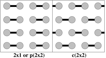
To establish baseline information which we shall need later, we computed ab initio energies for various reconstructions of the Si(100) surface. These calculations were carried out in a supercell geometry with slabs of twelve atomic layers containing 48 silicon atoms and separated by 9Å of vacuum. We sampled the Brillouin zone using the four k points . Among the 2x1, p(2x2), and c(2x2) reconstructions of the (100) surface (Figure 1), we find in good agreement with previous calculations[14] that the p(2x2) is lowest in energy with a binding energy of 1.757 eV/dimer, and that the 2x1 reconstruction is higher in energy than the p(2x2) by 0.114 eV/dimer. Furthermore, we find the c(2x2) reconstruction to be higher in energy than the p(2x2) by 0.154 eV/dimer. To determine the expected size of the facets along the edges of the bars we require the Si(100) and Si(110) surface energies. These are known experimentally to be 1.36 and 1.43 J m-2 respectively[15].
Our ab initio study of edges is carried out on bars with a cross section of cubic unit-cells in the (001) plane. We apply infinite periodic boundary conditions in the [001] direction with a periodicity of two cubic unit cells. The ball-and-stick diagram in Figure 2 depicts the projection of this structure on to the (001) plane. Ab initio calculations on the bars were performed using the same pseudopotential and energy cutoff as used above for the surfaces. For the bars, we sampled the Brillouin zone at the two k points and provided for a minimum of 6Å of vacuum between periodic images of the bars.
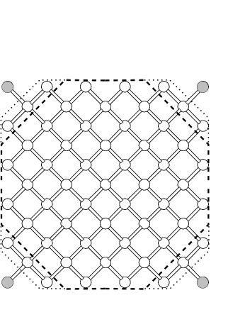
Prediction of a finite-size transition — Before determining the reconstructions along the edges and surfaces, we first must determine the overall cross-sectional geometry of the bar. To establish this, we performed the Wulff construction using the experimental surface energies given above. Figure 2 shows the resulting shape when {110} facets connect {100} surfaces of silicon, scaled to the lateral size of our bars. The atomic-scale structure most consistent with the Wulff construction in shape and aspect ratio appears in Figure 2, where we have removed the four columns of shaded atoms along the edges. The projection in the (001) plane of the final structure is an octagon. With the aforementioned periodicity along [001], the final structure contains 114 atoms. Without relaxation, all atoms on the surfaces of the bar are two-fold coordinated.
Having determined the overall geometry, we may now turn to the more subtle issue of relaxation and possible reconstructions along the surfaces and edges. We have found two competing structures: one which best satisfies the system in terms of the total number of bonds, and the other which best satisfies the system in terms of the configuration of the exposed surfaces. We find that the system cannot satisfy both conditions simultaneously.
Starting from the unrelaxed configuration, there is one unique surface atom with which each edge atom may bond in order to become three-fold coordinated. This bonding does not change the periodicity along the edge, which is the [001] vector of the crystal lattice. This periodicity, however, is incompatible with the periodicity of the p(2x2) low energy state of the {100} facets. To maintain maximal bonding, the arrangement of atoms on the {100} facets must then revert to the higher energy c(2x2) reconstruction. We denote this configuration of the bar as the “c(2x2) reconstruction” (See Figure 3).

While the c(2x2) reconstruction maximizes the number of bonds in the system, the increased energy represented by the c(2x2) arrangement on the {100} facets will eventually outweigh the benefit of maximal bonding along the one dimensional edges for a sufficiently large system. When the {100} facets assume the p(2x2) configuration, the periodicity along the [001] direction is doubled. The edge atoms are no longer equivalent, and every other atom now cannot form a new bond and remains only two-fold coordinated. Because of bonding restrictions into the interior of the structure, the dimer rows along alternate faces assumes a pattern which leads us to denote this configuration as the “2x1 reconstruction.” (See Figure 3.)
The ground state of the bar is thus determined by the balance between bonding along the edges and the surface energy of the facets. We find that for our bar the effects from the edges overcome the natural tendency of the surfaces. The c(2x2) configuration is lower in energy than the 2x1 configuration by 1.94 eV per [001] vector along the length of the bar. There is therefore a size-dependent transition in this system as we increase the lateral dimension of the bar and place relatively more atoms on the {100} facets. Our calculations place the crossover point at approximately 5 dimer pairs on each (100) surface per unit cell along [001], corresponding to a bar with cross sectional dimensions of approximately 3.0 nm 3.0 nm, far larger than the scale of an atomic cluster. We therefore predict an important edge-driven transition at a scale only two or three smaller than what has been achieved experimentally to date[1].
More generally, we can see that the compatibility of the competing surface reconstructions with the translational symmetry of the edges plays a pivotal role in determining the ground state of nanoscale structures. In our specific case, it is the principal physical mechanism giving rise to the size-dependent transition for our bars.
Implications of the transition— Comparing the electronic structures of the two reconstructions (see Figure 4), we find that the 2x1 configuration has a gap of 0.35 eV across the Fermi level. Furthermore, the topmost filled states consist of four nearly degenerate states which are localized on the four edges of the bars, and this cluster is separated from states below it in energy by a gap of 0.30 eV. This nearly symmetric placement with sizeable gaps as well as the spatial localization of the edge states leads us to conclude that the 2x1 bar is insulating.
On the other hand, the electronic structure of the c(2x2) configuration is more subtle. The states in the vicinity of the Fermi level are localized on the surfaces of the bars, and the gap across the Fermi level is only 0.09 eV. We believe the c(2x2) configuration is a small-gap semiconductor or even perhaps metallic. Thus the nature of the low energy electronic states and excitations differ between the two bars and should manifest themselves in physical measurements such as electrical conductivity or optical spectra.
Next, considering possible differences in mechanical properties, we carried out molecular dynamics simulations using a tight-binding model to compute transverse acoustic phonon frequencies for the bars. We believe that the tight-binding model will give us a qualitative view of the differences which may exist between the two bars. If any large differences are found, we should examine this issue in more detail using the more demanding ab initio techniques.
We used the semi-empirical tight-binding model of Sawada[16] with the modification proposed by Kohyama[17]. This model provides a good qualitative description of bulk, dimer, and surface energetics of silicon. In using the Sawada model, we only keep Hamiltonian matrix elements and repulsive terms between atoms closer than Å.
In order to calculate the band-structure energy, we used the fully parallelizable technique of Goedecker and Colombo[18]. By checking the convergence of the total energy to its ground-state value (determined by exact diagonalization), we found it necessary to use the following set of parameters to ensure convergence of energies to within an accuracy of eV/atom: in the nomenclature of [18], we have eV, , and Å.

Table 1 summarizes the results of the Sawada model for the various key physical values in this study. Although the Sawada model correctly predicts asymmetric dimers as the ground-state of the Si(100) surface, it is not sensitive to the delicate rocking of dimers that differentiates the 2x1 and p(2x2) reconstructions and hence finds the 2x1 reconstruction to be lower in energy than the p(2x2). However, in our study, the relevant energy difference is that between the c(2x2) and the lowest-energy reconstruction of the surface, and this quantity is reproduced rather well. The Sawada model also does well in predicting surface energies: Figure 2 shows the result for the Wulff construction when we use the tight-binding surface energies, and the resulting geometry is very similar to the experimentally derived one. Thus we believe that the Sawada model provides a good semi-quantitative description for the physics of our bars.
Using the Sawada model, we computed transverse acoustic phonon frequencies for the mode (along ) for both reconstructions of our bars, the longest allowed wavelength along the length of the bar consistent with the periodic boundary conditions. We ran molecular dynamics simulations using the Verlet algorithm with a time-step of 2.4 fs for 900 time steps. Phonon frequencies were identified as peaks in the frequency-domain power-spectrum of the velocity autocorrelation function as estimated by auto-regressive fits. We found frequencies of THz and THz for the c(2x2) and 2x1 configurations respectively. Thus we see that edge effects do not have a significant effect on the long wavelength vibrations of the bars.
Conclusions— We have performed an ab initio study of the energetics of long bars of silicon in vacuum. We found useful the atomic-scale version of the Wulff construction as a first step in determining nanoscale structure. Next, we found that one cannot ignore the interplay between the edges and surfaces in silicon structures with dimensions of a few nanometers, where the compatibility of the surface reconstructions with the symmetry of the edges plays an important role. In particular, the ground-state of our bars changes from one surface reconstruction to another, signalling a cross section-dependent phase transition, with significant influence on the electronic structure of the system. Finally, we find that even on the scale of a few nanometers, the surface-edge interplay has little effect on mechanical properties.
| Expt/Ab initio | TB | |
| Bulk properties | ||
| Binding energy (eV/atom) | -4.63a | -4.79 |
| Bulk modulus (Mbar) | 0.975a | 0.906 |
| Phonon frequencies | ||
| (THz) | 15.5b | 18.1 |
| LA (THz) | 3.9b | 3.8 |
| TA (THz) | 2.4b | 3.0 |
| Si(100) reconstructions | ||
| lowest energy (eV/dimer) | p(2x2): 1.757 | 2x1: 2.05 |
| c(2x2) (eV/dimer) | 1.603 | 1.93 |
| Surface energies | ||
| Si(100) (J m-2) | 1.36c | 1.44 |
| Si(110) (J m-2) | 1.43c | 1.77 |
| Differences between zizag and c(2x2) bars | ||
| Energy difference (eV/) | 1.94 | 1.57 |
| Cross-over (width in nm) | ||
Acknowledgments
We thank Prof. Alan Edelman, Matteo Frigo, Andrew Pochinsky, and Prof. John Negele for valuable discussions regarding optimization and parallelization of the computer code. We also thank Nicolaj Moll for providing us with Ref [15]. The calculations were carried out on the Xolas prototype SMP cluster. This work was supported primarily by the MRSEC Program of the National Science Foundation under award number DMR 94-00334 and also by the Alfred P. Sloan Foundation (BR-3456).
References
- [1] B.P. Van der Gaag and A. Scherer, Appl. Phys. Lett. 56, 481 (1990).
- [2] J. Ihm, D.H. Lee, J.D. Joannopoulos, and J.J. Xiong, Phys. Rev. Lett. 51, 1872 (1983).
- [3] J. Travis, “Building Bridges to the Nanoworld,” Science 263, 1703 (1994).
- [4] L. T. Canham, Appl. Phys. Lett. 57, 1046 (1990).
- [5] See for example: F. Buda, J. Kohanoff, and M. Parrinello, Phys. Rev. Lett. 69, 1232 (1992); M. S. Hybersten and M. Needels, Phys. Rev. B 48, 4608 (1993).
- [6] H. Yorikawa, H. Uchida, and S. Muramatsu, J. Appl. Phys. 79, 3619 (1996).
- [7] M. S. Hybersten, Phys. Rev. B 72, 1514 (1994).
- [8] Alex Zunger and Lin-Wang Wang, Applied Surface Physics 102, 350 (1996).
- [9] M. C. Payne, M. P. Teter, D. C. Allan, T. A. Arias, and J. D. Joannopoulos, Rev. Mod. Phys. 64, 1045 (1992), and references therein.
- [10] J. Perdew and A. Zunger, Phys. Rev. B. 23, 5048 (1981).
- [11] D. M. Ceperly and B. J. Alder, Phys. Rev. Lett 45, 566 (1980).
- [12] L. Kleinmann and D. M. Bylander, Phys. Rev. Lett. 48, 1425 (1982).
- [13] T. A. Arias, M. C. Payne, and J. D. Joannopoulos, Phys. Rev. Lett. 69, 1077 (1992).
- [14] N. Roberts and R. J. Needs, Surf. Sci. 236, 112 (1990); J. Fritsch and P. Pavone, Surf. Sci. 344, 159 (1995).
- [15] D. J. Eaglesham, A. E. White, L. C. Feldman, N. Moriya, and D. C. Jacobson, Phys. Rev. Lett. 70, 1643 (1993).
- [16] S. Sawada, Vacuum 41, 612 (1990).
- [17] M. Kohyama, J. Phys.: Condens. Matter 3, 2193 (1991).
- [18] S. Goedecker and L. Colombo, Phys. Rev. Lett. 73, 122 (1994).
- [19] C. Kittel, Introduction to Solid satate Physics, 6th edition. John Wiley & Sons, Inc.: New York, 1986.
- [20] G. Dolling. Inelastic Scattering of Neutrons in Solids and Liquids Vol. II (International Atomic Energy Agency, Vienna, Austria, 1963), p.37.