Quantum mechanical analysis of the elastic propagation
of electrons in the Au/Si system: application to
Ballistic Electron Emission Microscopy
Abstract
We present a Green’s function approach based on a LCAO scheme to compute the elastic propagation of electrons injected from a STM tip into a metallic film. The obtained 2D current distributions in real and reciprocal space furnish a good representation of the elastic component of Ballistic Electron Emission Microscopy (BEEM) currents. Since this component accurately approximates the total current in the near threshold region, this procedure allows – in contrast to prior analyses – to take into account effects of the metal band structure in the modeling of these experiments. The Au band structure, and in particular its gaps appearing in the [111] and [100] directions, provides a good explanation for the previously irreconcilable results of nanometric resolution and similarity of BEEM spectra on both Au/Si(111) and Au/Si(100).
pacs:
61.16.Ch, 72.10.Bg, 73.20.AtI INTRODUCTION
Ballistic Electron Emission Microscopy (BEEM)[2, 3] is a new technique based on the Scanning Tunneling Microscope (STM). It has been primarily designed for the study of buried metal-semiconductor interfaces, in particular for the investigation of the Schottky barrier. The experimental setup consists of a STM injecting current in a metallic film deposited on a semiconductor material. After propagation through the metal, a fraction of these electrons still has sufficient energy to surpass the Schottky barrier and may enter into the semiconductor to be finally detected as BEEM current. Using the tunneling tip as a localized electron source gives BEEM its unparalleled power to provide spatially resolved information on the buried interface, that can additionally be related to the surface topography via the simultaneously recorded tunneling current.
The energy of the electrons contributing to the final BEEM current depends on the bias voltage between tip and metal, and is typically 1 to 10 eV above the Fermi energy in the metal. For energies close to the threshold voltage (the ones of primary interest for exclusive Schottky Barrier Height (SBH) investigations), thin metallic layers, and low temperature, the main contribution to the BEEM current stems from the elastic component, which are electrons not having suffered losses from electron-electron and/or electron-phonon interaction. Only in this limit can the technique be properly called ballistic [4], and we shall concentrate in this paper on the propagation of such electrons and their contribution to the BEEM current.
The Au/Si interface has been one of the first systems investigated by BEEM and has also proven to be a controversial one. Two important and apparently irreconcilable results have been (i) the elegant demonstration of nanometric resolution (Å) after propagation through films of as much as Å [5], and (ii) the very similar results obtained for the interfaces with Si(111) and Si(100) [2, 6, 7] despite the strongly different k-space distribution of the projected Conduction Band Minima (CBM) available for injection of electrons into the semiconductor.
The theoretical analysis of BEEM data is usually based on the so-called four step model [3]: 1) tunneling from the tip to the surface, 2) propagation of the electrons through the metallic layer, 3) injection into the semiconductor and 4) effects associated to various current-changing processes in the semiconductor (e.g. impact ionization and/or creation of secondary electrons). The last process becomes, however, only important at rather high energies and can be safely neglected when concentrating on the near threshold regime. The standard model used to extract SBH’s from the experiment is a simple quasi 1D semiclassical approximation using planar tunneling theory and WKB approximation for step 1), free electron propagation plus simple exponential attenuation for step 2) and the QM transmission coefficient derived for a 1D step potential for step 3). This predicts a 5/2-power law for the onset of the BEEM current above the threshold energy and has been used extensively for the fitting of experimental data [3].
Despite its obvious merits and especially its highly welcomed simplicity, the standard model fails for more than a mere qualitative explanation of experimental data. In particular, the above mentioned results for the Au/Si system are not comprehensible within the framework of this crude approximation. As has been pointed out recently [8], the major error leading to these discrepancies for Au/Si is the complete neglect of band structure effects inside the metal film. The free electron treatment of the existing model predicts an electron beam propagating in normal direction through the metal film, grown in [111] direction on either Si(111) or Si(100) [9, 10]. On the other hand, it is a well known that Au shows a band gap in just this direction [11], i.e. the Au band structure clearly forbids electronic propagation normally through the film.
Unfortunately, the inclusion of band structure effects into a theoretical model requires a much higher level of sophistication than for the previous simple approximation based on E-space Monte-Carlo and various parametrized processes. We therefore present in this paper a Linear Combination of Atomic Orbitals (LCAO) scheme for the fully quantum mechanical computation of the elastic component of the BEEM current: step 1) is included by coupling the tip to a semi-infinite crystal via the Keldysh Green‘s function formalism [12], whereas for step 2) we can take the Au band structure fully into account via the corresponding Slater-Koster parameters [13, 14]. This concept allows to compute the electron current distributions in real and reciprocal space in any layer inside the metal film.
We will show in this paper, that already the detailed analysis of these 2D distributions immediately resolves the previously puzzling results for Au/Si as a pure consequence of the band gap enforced sideward propagation of the electron beam inside the metal film. This sideward beam is highly focused thus explaining the obtained nanometric resolution, but it is also dominated by electrons with rather high -momentum parallel to the interface, which allows similar injection into the projected Si CBM for both Si(111) and Si(100) interfaces. Even though our proposed model is a little more demanding than the old simple one both from a theoretical and a computational point of view, we believe that it allows to gain deeper insight into the physics involved and that it represents a step towards a more careful treatment of the BEEM process which ultimately will enable a much better use of the obtained experimental data.
II THEORY
Our model is based on a Hamiltonian written in a LCAO basis:
| (1) |
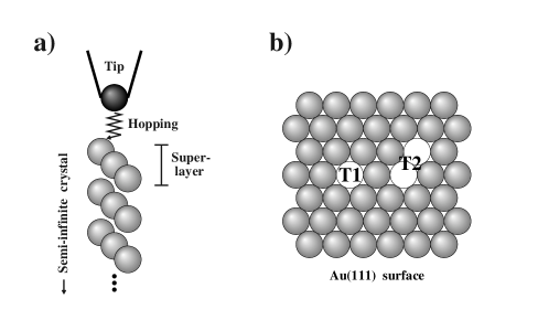
where defines the tip, designates the metal sample and describes the coupling between the tip and the surface in terms of a hopping matrix, (, , and are number, creation and destruction operators defined in the usual way). Note, that greek indices indicate tip sites, whereas latin indices correspond to sites inside the sample. The tight-binding parameters allow us to fully take into account the sample band structure and can be obtained within the empirical tight-binding framework by a fitting to ab-initio band structures [13]. Tabulated values exist for all elemental crystals, in particular for Au as used in the present paper [14]. The hopping matrix between tip and sample is also expressed as a function of the different atomic orbitals of atom in the tip and atom in the sample. Since BEEM experiments operate at high bias and rather low current, where the tip-surface distance is already of the order of Å, only tunneling between s-orbitals needs to be considered without loss of generality. The actual matrix element for this tunneling between the s-orbitals is simply described by an exponential function, as derived from the WKB approximation [15]. It is important that is localized in a small region of atoms close to the tip.
A Green’s function formalism presents the important advantage of being free of any adjustable parameters in the strictly elastic limit, where only an arbitrarily small positive imaginary part is added to the energy, , necessary to ensure mathematical convergence:
| (2) |
Although in this paper we are not interested in discussing inelastic effects, which will form part of a forthcoming paper, it is worth mentioning that a finite can be used to give some attenuation to the wavefield, mimicking inelastic effects that draw away current from the BEEM experiment. We shall see in the discussion of the k-space current distributions that a finite effectively defines a coherence region of size approximately given by . Inside this region, quantum mechanical effects are important, but outside of it quantum coherence is lost and intensities rather than amplitudes should be added to compute the final wavefield.
The system under investigation is out of equilibrium as soon as a bias between tip and sample is applied[16]. In order to retain the ab-initio advantage of a Green‘s function formalism, but still to be able to couple the tip to the sample, it is convenient to use the Keldysh technique [12], which essentially represents the generalization of many-body Green‘s function theory to systems out of equilibrium [17]. Within this formalism, the current between two sites and in the sample can be written as:
| (3) |
The matrices are non-equilibrium Keldysh Green’s functions that can be calculated in terms of the retarded and advanced Green’s functions / of the whole interacting tip-sample system. We are interested only in the elastic component of the current,
| (4) |
where is the coupling between tip and sample that can be build up from the hopping matrices, , linking atoms in both subsystems, while refers to the Keldysh Green’s functions of the uncoupled parts before any interaction has been switched on.
The retarded and advanced Green’s functions of the interacting system can be further obtained from a Dyson-like equation that uses the Green’s functions of the uncoupled parts of the system, /, and the coupling between the surface and the tip, :
| (5) |
After some algebra, it is shown in Appendix A that the current between two sites and in the metal can be obtained, in the lowest order of perturbation theory with respect to the coupling between tip and sample, from the following formula:
| (6) |
where the integration is performed between the Schottky barrier () and the voltage () applied between the tip and the sample. We notice that this equation shows spectroscopic sensitivity because the Green’s functions, , and the hopping matrices, , depend on the energy, and also through the upper limit in the integral. The summation runs over tunneling active atoms in the tip (, ) and the sample (, ), is the density of states matrix: . The trace denotes summation over the atomic orbitals forming the LCAO basis.
Note, that the detour via the Keldysh technique has enabled us to arrive at an expression that only includes the (tabulated) tight-binding parameters inside the sample, the hopping elements / between tip and sample, and the retarded and advanced equilibrium Green‘s functions / of the isolated tip and sample.
We shall describe the injection of electrons from the metal into the semiconductor simply by matching the corresponding states. Therefore, we shall need to compute the current distribution at the interface in reciprocal space. Working in a similar way as above for the real space, we find the following expression for the current distribution in reciprocal space defined now between planes and :
| (7) | |||||
| (8) |
where in this case the sum runs over layers in the tip (, ) and sample (, ) that are involved in the tunneling process. All quantities in eq. (8) are the -Fourier transforms of the corresponding objects in formula (6). The total current between planes and can be obtained by summing the current distribution as obtained in eq. (8) over the 2D Brillouin zone.
It is worth mentioning, that even though the total resulting current at the given STM bias is obtained as an integral in energies down to the SBH, the dominant contribution will be just the one at itself, due to the strong exponential dependence of the tunneling coupling terms with energy. This shall allow us to present qualitative results displaying only this main contribution (calculated at the highest energy, ), although we have additionally verified that essentially the same effects occur at lower energies.
¿From equation (6) it is clear that the main objects of interest that still need to be calculated are the retarded and advanced equilibrium Green‘s functions / for a metallic surface. We compute these quantities using a decimation technique [20, 21], which involves an iterative process allowing in each step to double in size an existing slab (the so-called ”superlayers” in Figure 1a). Assuming perfect periodicity in both directions parallel to the surface one can easily calculate , the retarded Green’s function of the surface superlayer which contains the tunnel-active layers . The layer doubling of the slab is then repeated until its size is so large, that the two surfaces are effectively decoupled. Hence, we obtain the Green‘s function projected at the surface, , and the transfer matrix of the system[19]. With these two quantities it is possible to calculate the Green’s function , representing the propagation of an electron of momentum and energy from the surface superlayer up to the layer inside the semi-infinite crystal. The corresponding Green’s function in real space is subsequently obtained by Fourier transforming:
| (9) |
where the summation is performed over N special points [22] in the 2D Brillouin zone with respective weights . Finally, it is straightforward, to obtain the corresponding advanced Green‘s function by transposing and conjugating:
| (10) |
Let us draw our attention to the full quantum-mechanical calculations in real space based on equation (6) and the decimation technique. The total procedure outlined in this section enables the computation of 2D current distributions at any layer inside the semi-infinite crystal. Using eq. (6), and calculating for all atoms inside a given layer, with current contributions from all their respective neighbours in the layer above, we arrive at the current distribution in real space. This simulates the BEEM current impinging on the semiconductor after propagation through a metallic film with a thickness corresponding to the chosen layer . Results of this type will help us to understand which spatial resolution can be expected in a BEEM experiment. Alternatively, the calculation of according to eq. (8) provides the current distribution between layers and inside the 2D projected Brillouin zone. Since ultimately the electrons need not only to have sufficient energy to enter the semiconductor as BEEM current, but also to have the corresponding to get into the Si CBM, this type of plot will permit us to investigate the onset and strength of the BEEM current for a certain type of interface.
When concentrating on the near threshold region, i.e. injection into the bottom of the Si conduction bands, the latter may be approximated by free electron-like paraboloids with appropriate effective masses[11]. In the 2D projection on either the Au/Si(111) or Au/Si(100) interface this will then lead to a number of ellipses inside the Brillouin zone, representing areas through which transmission into the semiconductor is possible [26]. To arrive at quantitative results, additionally a QM transmission factor for each of the matched states has subsequently to be applied. However, in the present paper we shall be concerned rather with qualitative results apparent from the 2D distributions themselves, and may thus leave the question of modeling the transmission factor for a forthcoming publication [27]. We feel that more physical insight is gained by visually comparing how the current distribution in the metal matches the available states in the semiconductor, than by presenting the final BEEM current, which results from a summation over all states with right matching conditions inside the 2D Brillouin zone. Therefore, in this work we simply draw in the 2D Brillouin zone the Si CBM ellipses to aid the eye identifying the relevant regions. We stress that the final summation tends to smooth details and, as the physically measurable observable is only the -integrated curve, this might be one reason that helps to explain why the previous simple models achieve in many cases decent fits to the data, even though it is quite obvious that the underlying 2D current distribution is grossly inconsistent with the metal band structure.
III Real space results
We apply our quantum-mechanical formalism to describe the elastic propagation of electrons through a [111]-oriented Au metallic layer. Due to the large lattice mismatch between Au (Å) and Si (Å)[28], the formed interface is of rather poor quality. Although the growth of Au layers on Si has not yet been studied extensively, there is evidence from Low Energy Electron Diffraction and Auger studies, that suggest that Au films growing either on Si(111)[9] or on Si(100)[10] form crystals oriented in the [111] direction after the first four or five layers, which typically display heavy disorder, are completed. From the nature of our results, that show the gradual build-up of Bloch waves as a function of the distance to the surface, we deduce that the likely disorder contained in four or five layers immediate to the interface, does not provoke the automatic destruction of the formed pattern. We therefore take the calculated 2D distributions in any given layer of the ideal semi-infinite crystal as a good approximation to the actual current arriving at the Si semiconductor after propagation through a Au film of corresponding thickness and passage through the disordered interface region.
Before discussing our full quantum-mechanical results, it is worth analyzing the semiclassical limit, which is based on Koster’s approximation to compute the bulk Green’s functions[23] and an appropriate symmetrization of waves reflected at the surface[24]. The central point in this semiclassical approach mainly valid for thick layers is that it admits a simple geometrical interpretation for the bulk propagators, relating them to the shape of the constant energy surface (Fermi surface) of the metal band structure: applying a stationary phase condition all -values contributing to the final Green’s function may be neglected except one particular [23]:
| (11) |
where , are the two principal curvatures associated with the constant energy surface and the eigenvectors , are obtained diagonalizing the bulk tight-binding Hamiltonian .
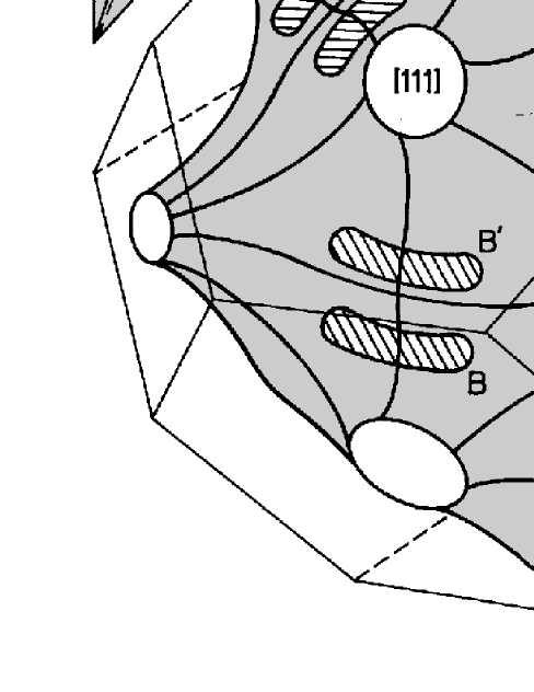
For a given propagation direction , is the vector linking the -space origin to the point on the constant energy surface (defined by the energy ) whose perpendicular to the surface is parallel to the initially chosen direction in real space (see inset in Fig. 2). This vector perpendicular to the constant energy surface at represents the group velocity of electrons being propagated in the metal, , that needs not to be parallel to when the metal band structure deviates from the free electron limit. Eq. (11) reveals that the current intensity is strongly enhanced in directions corresponding to rather flat parts of the constant energy surface, where the principal curvatures and in the denominator tend towards zero (note, that at the extremal points, where the second derivatives are exactly zero, the next term in Koster’s expansion is needed). Hence, already a simple visual analysis of the constant energy surface’s shape may provide an intuitive understanding where major ballistic current contributions are to be expected when including band structure effects.
As pointed out previously[8], for the analysis of electron propagation in Au layers at typical BEEM energies, it is crucial to notice that for voltages larger than V necks develop in the [100] directions, which are similar to the well known necks in the [111] directions, cf. Fig. 2. Identifying the flat parts on this surface and their corresponding real space propagation directions, we were able to make a qualitative prediction of the current distributions in real and reciprocal space after propagation through a thick Au film[8].
In Fig. 2, we have drawn the Au constant energy surface for 1 eV above , and the regions (dashed areas) giving the major contribution to the semiclassical BEEM current in k-space. One of these areas is also shown in the figure inset: the reason why the k-space current distribution maximum is associated with the A-region, and not with the apparently equivalent A’-region, is their different orientation w.r.t. the (111)-direction (see. Figs. 6 and 8). It should be kept in mind that the dashed areas of Fig. 2 define the momentum and velocity components of the electrons contributing most to the BEEM-current: the group velocity defining the semiclassical propagation in real space. Since most BEEM modeling up to now has been performed using E-space Monte-Carlo techniques, it may be interesting to notice, that apart from the neck regions where no propagation is possible, the Au constant energy surface remains spherical to a good approximation (Fig. 2): the group velocity perpendicular to the surface and the connecting k-vector do not diverge by more than for most directions of interest outside the necks. When properly suppressing the forbidden propagation directions corresponding to the necks, a simple application of k-space Monte-Carlo simulation should thus be possible, resulting in analogous results to ours in the purely ballistic limit. This allows the simulation of inelastic interactions in an approximate but simple way through the inclusion of the appropriate k-space scattering cross sections, reaching the interesting conclusion that those effects do not significatively degrade the elastic predicted resolution in real space[25].
The presented semiclassical approach helps to better understand the numerical results in terms of the geometrical interpretation. However, we have also at hand the quantum mechanical decimation technique for the computation of the Green‘s functions, which allows us to precisely calculate these distributions and also not only for thick films, but for any thickness. Since we are only interested in the qualitative evolution of injected current in a [111]-oriented Au film, we start with a simplified tunneling geometry, in which hopping is only permitted between one tip atom and one sample atom positioning the tip directly on top of the latter at Å distance, cf. Fig. 1b. More realistic tunnel geometries allowing hopping to more atoms lead to essentially the same results: one advantage of properly taking the metal band structure into account is that the results are not that much dependent on the initial tunneling conditions as long as metallic films of a certain thickness are involved. This is a strong difference between our theory and the standard ballistic E-space Monte-Carlo approach. The k-space distribution arriving at the semiconductor under the assumption of free electron propagation is inappropriate for both very thick and very thin layers: (i) it is physically unreasonable to assume that what impinges on the interface (after a long propagation through the metal) is just the initial tunneling distribution, and (ii) on the other hand, when the film is thin enough for the details of tunneling to become important, the crude planar theory based on WKB should not be applied. On the contrary, in all the examples presented in this paper (where we have deliberately avoided ultra thin layers), tunneling simply provides a starting configuration, whereas the final current distribution at the interface is dominated by the preferred propagation directions dictated by the metal band structure. In any case, should the initial tunneling distribution become important for some particular application, our formalism would permit a more realistic point of view for that part of the problem.
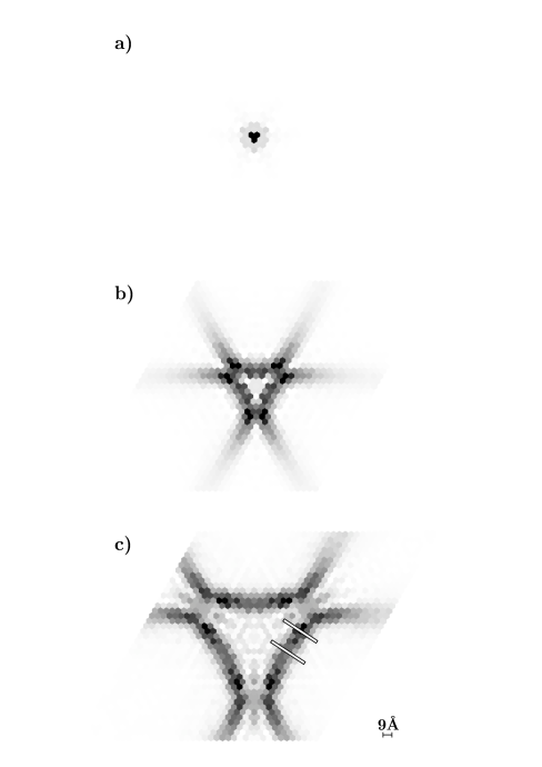
This discussion is illustrated in Fig. 3, where the resulting real space current distribution after electron propagation through more and more layers is depicted. As electron energy we chose 1 eV above the Fermi level of the metal. 2971 special k-points were used inside the 2D Au Brillouin zone to suppress possible aliasing effects in the involved Fourier transforms to real space. In the second layer, very near to the surface (Fig. 3a), the current is still strongly concentrated in the atoms closest to the location in the surface layer in which the current was injected. This behaviour, where the current still propagates in all directions and where the resulting distribution is basically a consequence of the crystal geometry and nearest neighbour hopping, can be found down to about the fifth layer. Then, however, an interesting change occurs, which is related to the gradual formation of a Bloch wave inside the crystal: propagation becomes only possible in directions in accordance with the metal band structure. The immediate consequence of the already mentioned band gap of Au in the [111] direction is that the evolving beam has to make way sidewards. This becomes obvious in Fig. 3b, where the opening up of the injected beam can already be observed with very little current remaining in the central plane atoms lying in the [111] forward direction.
A further effect of the band structure is the formation of narrowly focused, Kossel-like lines corresponding to preferred propagation directions. After propagation through a larger number of layers, a steady state is reached and distributions for consecutive layers differ only by the natural spreading of the resulting triangle as the electrons follow these preferred propagation directions of the band structure, cf. Fig. 3c. These directions have a polar angle of about with respect to the normal direction, and are in good agreement with our previous semiclassical analysis[8] (see Fig. 2). Note, how different the resulting pattern in each layer is from the prediction of the simple, free electron model: there the propagation would be solely dictated by the -spreading of the initial tunneling distribution resulting in a current cone centered around the [111] direction. Consequently, the real space distribution in any layer parallel to the surface would be a filled circle (or rather a filled triangle, considering the symmetry of a fcc (111) crystal [29]) with the major current contributions directly in the middle corresponding to normal propagation through the metal film.

The deeper the chosen layer, i.e. the larger the thickness of the experimental film, the more spread over a larger triangle the current would be. The simple application of the uncertainty principle to the tunneling process plus a free electron model for the metal [5, 6] predicted a BEEM resolution for relatively thick Å Au films of at best Å. On the contrary, the experiment by Milliken et al. [5] finds typical resolutions for such films on both Si(111) or Si(100) of about Å. In that experiment, sharp SiO2 steps are created on both Si substrate types and subsequently covered by Å Au films. BEEM images of the step riser, when the tip crosses from above a part corresponding to the impenetrable SiO2 to a part, where BEEM injection into the Si is possible, give a direct reflection of the size of the electron beam at the interface. The typical Å found are absolutely incompatible with the standard ballistic, free particle propagation used in the simple model and are difficult to justify even if parametrized electron-electron/electron-phonon interaction is taken into account[5, 6]. On the other hand, we believe that the observed formation of narrowly focused Kossel-like lines as caused by the Au band structure may already explain the experimentally obtained nanometric resolution in the purely elastic limit. As can be seen in Fig. 3c, the width of these lines carrying the BEEM current is typically 3-4 atomic distances. This is better appreciated in Fig. 4, where cuts perpendicular through these lines at two different positions were performed and the intensity vs. location is depicted. The derived width of Å is in very good agreement with the experimentally observed value and is clearly distinct from the value derived from free electron theory, which deviates by a complete order of magnitude.
A naive interpretation of this result seems to imply that multiple images of interface objects should be observed superimposed, since several such Kossel-lines are present in our distribution. A tip scan would sweep each of these lines across the interface object, each time leading to a focused signal. It should, however, be born in mind, that so far we have used unrealistically symmetric conditions for the current injection process: the on top tip site used, allows the current pattern to display the full threefold symmetry of the fcc crystal[29] and hence predicts the existence of three equivalent Kossel-like lines. During the scan, less symmetric tip sites are on the contrary involved, reducing logically the resulting overall symmetry of the current distribution. To verify this, we repeated the calculation, this time using a bridge site for the tip and allowing tunneling to both closest atoms on the surface, cf. Fig. 1b.
Several conclusions can be drawn from the result shown in Fig. 5, which is for the limiting case after propagation through already a thick film. First, as expected, the overall symmetry of the pattern has reduced from threefold to twofold, with one of the three Kossel-like lines decreasing in intensity. Second and most importantly, the shape of the distribution has essentially not changed. This is the confirmation of the introductory statement made at the beginning of this section: the inclusion of band structure effects reduces considerably the influence of the initial tunneling distribution. The preferred directions of propagation are exclusively dictated by the band structure, whereas it is only the population of these directions with electrons that depends on the actual tunneling process. In this respect, we again observe in Fig. 5 the off-normal, sideward propagation along focused lines, of which now only the two corresponding to the chosen tunnel symmetry are mainly populated.
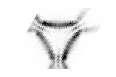
As we are interested in highlighting the relevant physical phenomena, we have introduced convenient approximations: one atom tip, spherical s-wave tunneling and a perfect substrate without any tilt, nor defects on the surface. In turn, the model neglects a number of factors that necessarily would result in a lower symmetry than the one existing in a realistic experimental setup. However, it is plausible to accept that different factors concur in the experiment to degrade symmetry, and will eventually lead to the selection of only one of the possible Kossel-like lines, whose dominant contribution will then be responsible for the observed BEEM image with its nanometric resolution. On the other hand, none of the experimental influences can change the metal band structure itself (as long as there are at least crystal grains of the order of 100Å), so that the formation of focused Kossel-like lines will be very similar to the one seen in our idealized model calculations.
IV Reciprocal space results
In order to understand how the current distribution in the metal matches the available states in the semiconductor, we now proceed to calculate the 2D distributions in reciprocal space using expression (8). Fig. 6a shows the result obtained inside the Au Brillouin zone, again for the symmetrical on top tip site, cf. Fig. 1b, and for an electron energy of eV, which is still near the threshold region for Au/Si. As a direct reflection of the Au [111] band gap, which projects onto in the center of the hexagon, the distribution displays a ring-like structure, since there are no states to carry the current in the vicinity. It is again interesting to notice, how different this pattern is from the free electron prediction, that would inject the main current with just into . In reality, complete reflection occurs for tunnel electrons with , permitting only injection into the Au(111) states of rather high -momentum.
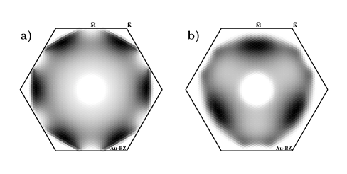
We would like to stress that the use of the decimation technique, which was derived from renormalization group techniques [20], permits the fully quantum mechanical calculation of both required Green‘s propagators / of the semi-infinite slab. The resulting BEEM current is consequently also fully quantum mechanical. It is therefore not surprising that the distribution shown in Fig. 6a possesses a sixfold symmetry, which relates to the symmetry of the [111] projected density of states to which and states contribute equally [30].
This is at variance with a semiclassical distribution, where only -vectors representing propagation towards the interface must be considered. These waves are classically separated from those that propagate in the opposite direction and the total vector field has thus the same symmetry as the constant energy surface, which in turn reflects the symmetry of the lattice, i.e. threefold for [111] directions in a fcc material [11]. Hence, our previous semiclassical approach yielded threefold symmetric BEEM current distributions [8].
As has already been mentioned in section II, the use of a finite self-energy in the construction of the Green‘s functions (2) puts some limits on the coherence length of our quantum mechanical computation. In the purely elastic limit, corresponding to a theoretical in eq. (2), the obtained distribution would not change at all after propagation through an infinite number of layers. In the ideal crystal, there are simply no processes enforcing -changes of the elastic electrons after their injection. Numerically, we are however forced to choose a small, but finite to ensure convergence. The result presented in Fig. 6a was hence obtained for eV, which is very small compared to the energy eV considered, and corresponds to a coherence length of several thousand Ångstrøm. No significant changes of the distribution can be observed during the propagation through many layers. Since in this case we are always well inside the coherence region, the symmetry is sixfold, as it should be for a quantum mechanical calculation.

On the other hand, we can considerably reduce the coherence length by using a much larger value for the optical potential, say eV. There would then exist a regime outside the coherence region where interference terms do not play a significant role any more. This should allow us to recover the semiclassical results. Fig. 6b shows the obtained distribution for such a large and for the 30th layer in the crystal, i.e. well outside the coherence region. It is most gratifying that not only the expected threefold symmetry appears, but that also the actual pattern matches perfectly with our semiclassical prediction, that was then only derived schematically, cf. Fig. 3 of ref. ([8]). Moreover, it is interesting to notice how our Green‘s function calculation permits to reproduce the involved change in symmetry: even for a large , propagation in the first layers is still inside the small coherence region and thus quantum mechanical effects are observed to produce the corresponding sixfold symmetry. During the propagation through more and more layers, the quantum coherence is gradually lost as is the symmetry, which progressively approaches its threefold limit. This allows to study the crossover between the quantum and the semiclassical domain and provides another example of how a quantum system, under the influence of friction, becomes classical by a decoherence process [31].
Note, that the change in symmetry implies also a change of the detailed current distribution itself: the maxima of the semiclassical pattern appear on the lines , whereas the quantum mechanical maxima lie along the directions . This is more obvious in Fig. 7, where an intensity cut along the symmetry lines is presented: the relative weight between currents along and respectively is inversed between the two types of calculations, which is a reflection of the symmetry change. It is interesting to notice that the evolution from the quantum symmetry to the classical one is gradually build up, and no sudden change between both regimes is found. Our calculations showed that the observed difference in reciprocal space does not significantly affect the beams in real space (where the symmetry must always be threefold), but it could nevertheless in principle affect the I(V) current injected through the projected ellipses into the semiconductor. However, because of the gradual crossover, no dramatic effects are to be expected, unless one could experimentally break the time-reversal symmetry suddenly (e.g. by application of a magnetic field).
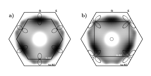
As a final point we address the actual transmission of the current into the semiconductor states. The chosen energy eV is still in the near threshold region (eV, eV [3]) justifying to approximate the Si CBM by nearly free electron ellipsoids. Since Si is an indirect semiconductor, these ellipsoids are not located around in the Brillouin zone, but ca. 85% in direction [11] and hence project differently onto the [111] and [100] directions [3, 26]. The resulting ellipses for both orientations are drawn in Fig. 8a and 8b. Note, that since we are calculating inside the larger Au Brillouin zone, those ellipses belonging to higher Si Brillouin zones, but still within the first Au one, have to be considered for current injection as well. The principal difference for both Au/Si(111) and Au/Si(100) interfaces is that in the latter case Si ellipsoids project directly onto , which is where the simple free electron picture puts the maximum current. Since very little current carried by electrons with high -momentum is predicted in this type of model, a considerable difference in the onset and absolute magnitude of the BEEM current was originally anticipated between both interfaces [3, 6]. On the contrary, the actual, experimentally observed spectra were highly similar [2, 6, 7]. Since this result was irreconcilable with the ballistic free electron theory, a variety of processes ranging from more isotropic tunnel distributions [5] over strong elastic electron-electron interaction [6] to -violation at the non-epitactic interfaces [32] were proposed in an extensive debate in the literature. All these processes aimed at providing -momentum to the current distribution to allow injection into the off-normal [111] ellipses, but ran into considerable trouble through the simultaneous, inherent loss of resolution [5].
On the other hand, the ring-like current pattern predicted by our band structure calculation is dominated by high -momenta, (cf. Fig. 8) but without loss of resolution, as we have seen in the last section. The total reflection of the injected electrons around due to the projected Au band gap renders the existence or non-existence of a Si ellipse in that region completely irrelevant, since no current can enter through it into the semiconductor in any case, and the current is therefore forced to enter via any of the off-normal ellipses for both Au/Si(111) (Fig. 8a) and Au/Si(100) (Fig. 8b). The ring-like distribution may in zeroth order be well described as azimuthally symmetric, making it highly plausible why the BEEM current shows similar onset and magnitude: the exact location of the off-normal ellipses plays only a minor role.
Finally, we quantify this result by comparing the actual current injected into the (100) and (111) silicon orientations. As mentioned in the beginning, we shall not get at this stage into the separate problem of computing a suitable transmission coefficient to keep our discussion as simple as possible. Hence, we simply use , which is justified because we shall only present the ratio between the current injected into both silicon faces , where factors not very sensitive to a particular silicon orientation cancel out. In particular, this is the case for the transmission coefficient as can easily be checked with the crude 1D step-barrier approximation[3]. Similarly, we do not need to consider inelastic effects, that are anticipated to affect equally electrons approaching the Si(100) or the Si(111) surface, and should in general be small when considering thin metal films. The ratio shown in Fig. 9 compares well with the experimental ratio obtained from refs. ([33, 34]), reproducing not only the correct order of magnitude, but also the overall trend with energy. The largest difference of 30% is seen in the low voltage region where experimental currents are weak and difficult to measure, and where the total current depends most sensitively on the exact value of the SBH for both orientations, whereas we have made no effort in fitting these values, but have simply taken averages over the big number of existing experimental values (which differ easily by 0.1 eV). It is hence not surprising that the agreement in the lowest 0.2 eV above the SBH is not as convincing as it is at the higher voltages. Taking finally into account the crudeness of the applied model where we have deliberately avoided the fitting of any parameter to focus on physical insight, we believe that the presented ring-like distribution provides a satisfactory and intuitive explanation of the observed effect.

V Conclusions
In conclusion, we have presented a theoretical model that allows the calculation of the elastic contribution to the BEEM current in the near threshold range. Based on a LCAO scheme and a Keldysh Green‘s function formalism, 2D distributions in real and reciprocal space may be computed in any layer of a semi-infinite crystal after current is injected from a tip atom. Subsequent matching with the semiconductor states permits to extract the actual BEEM current, although the main emphasis in the present paper has been on the qualitative understanding that can already be obtained from the 2D patterns themselves. The model allows for the first time to fully take into account the influence of the metal band structure in the BEEM process, and possesses the further advantage of being free of any adjustable parameter in the strictly elastic limit.
The application to the system Au/Si shows a variety of consequences of the Au band gap in the [111] direction. In real space, the formation of narrowly focused Kossel-like lines and a sideward beam propagation is observed, which may explain the experimentally obtained nanometric resolution. In reciprocal space, a symmetry change between quantum mechanical and semi-classical regime can be related to the gradual breaking of quantum coherence. The actual pattern in k-space has a ring-like shape, which calls for current injection via the off-normal Si ellipses for both Au/Si(111) and Au/Si(100). Hence, the sole inclusion of band structure effects achieves to explain the nanometric resolution and the similarity of BEEM spectra on both Si orientations on the same footing in the purely elastic limit – without any adjustable parameter and without the necessity to invoke any further scattering process.
Acknowledgments
K.R. is grateful for financial support from SFB292 (Germany). We also acknowledge financial support from the Spanish CICYT under contracts number PB92-0168C and PB94-53.
APPENDIX A
We start from formula (3) and the Keldysh Green’s functions defined in (4). The coupling term can be expressed as a function of the real hopping matrices, , that link tunneling active atoms in the tip () with the corresponding ones in the sample ().
Using equation (4), and can be written as:
| (13) | |||||
| (15) | |||||
The Keldysh Green‘s function of the uncoupled (and hence equilibrium) system can be expressed as a function of the advanced and retarded Green’s function of the uncoupled parts / and the Fermi distribution functions of the tip, , and sample, :
| (16) | |||||
| (17) | |||||
| (18) | |||||
| (19) | |||||
| (20) |
Using these last equations we obtain:
| (21) |
where we have defined the auxiliary variables:
| (23) | |||||
and
| (25) | |||||
The term in (21) gives a zero contribution to the current because it corresponds to the current between sites and inside the metal in the absence of tip-sample coupling, which obviously must be zero.
Let us work now with the term associated to the tip, . This term can be simplified by using the well known relation between advanced and retarded Green’s functions: . The real matrix is just equal to . Hence:
| (26) | |||||
| (27) |
So can be expressed as the real part of a matrix:
| (28) |
The retarded and advanced Green’s functions for the interacting system can further be obtained from a Dyson-like equation that uses the Green’s functions of the uncoupled parts of the system / and the coupling term / (equation 5):
| (29) |
If the values of the coupling matrix are much smaller than hopping terms inside the metal (as it is the case in tunneling conditions) we can work in the lowest order perturbation theory and approximate and simply by and , respectively. Moreover, we can further simplify the expression for by relating with the density of states matrix at the tip by the equation :
| (30) |
The term associated with the sample, , can also be written as the real part of a matrix using similar arguments leading to (28):
| (32) | |||||
Using the Dyson-like equation for the Green’s functions of the interacting system and again working in the lowest order of perturbation theory:
| (33) |
| (34) |
The term associated with the sample can then be expressed as:
| (36) | |||||
It is easy to demonstrate that the first term of this equation is zero because it is the real part of the difference of two magnitudes, one being the complex conjugate of the other. Hence can be shortened to:
| (37) |
So the rest between and is finally written:
| (38) |
Assuming zero temperature, we obtain the current between two sample sites and in the sample as an integral over a window of energies ranging from the Schottky Barrier Height () up to the applied voltage of the imaginary part of the trace of a product of matrices:
| (39) |
This is equation (6), that can be considered as our starting point.
REFERENCES
- [1] On leave from: Lehrstuhl für Festkörperphysik, Universität Erlangen-Nürnberg, Germany.
- [2] W.J. Kaiser and L.D. Bell, Phys. Rev. Lett. 60, 1406 (1988); L.D. Bell and W.J. Kaiser, Phys. Rev. Lett. 61, 2368 (1988).
- [3] L.D. Bell and W.J. Kaiser, Annu. Rev. Mater. Sci. 26, 189 (1996); M. Dähne-Prietsch, Phys. Rep. 253, 164 (1995).
- [4] P.L. de Andres, K. Reuter, F.J. Garcia-Vidal, D. Sestovic, and F. Flores, Appl. Surf. Sci. 123, 199 (1998); cond-mat/9710091.
- [5] A.M. Milliken, S.J. Manion, W.J. Kaiser, L.D. Bell, and M.H. Hecht, Phys. Rev. B 46, 12826 (1992).
- [6] L.J. Schowalter and E.Y. Lee, Phys. Rev. B 43, 9308 (1991).
- [7] R. Ludeke, Phys. Rev. Lett. 70, 214 (1993).
- [8] F.J. Garcia-Vidal, P.L. de Andres and F. Flores, Phys. Rev. Lett. 76, 807 (1996).
- [9] A.K. Green and E. Bauer, J. Appl. Phys. 47, 1284 (1976).
- [10] K. Oura and T. Hanawa, Surf. Sci. 82, 202 (1979).
- [11] N.W. Ashcroft and N.D. Mermin, Solid State Physics, Saunders College, Philadelphia (1976).
- [12] L.V. Keldysh, Sov. Phys. JETP 20, 1018 (1965).
- [13] J.C. Slater and G.F. Koster, Phys. Rev. 94, 1498 (1954).
- [14] D.A. Papaconstantopoulos, Handbook of the band structure of elemental solids, Plenum, New York (1986).
- [15] C.J. Chen, Introduction to Scanning Tunneling Microscopy, Oxford Univ. Press, Oxford (1993).
- [16] C. Caroli, R. Combescot, P. Nozieres, and D. Saint-James, J. Phys. C 5, 21 (1972).
- [17] E.M. Lifshitz, L.P. Pitaevskii, Physical Kinetics, Course of Theor. Phys. Vol. 10, Pergamon Press, Berlin (1981).
- [18] F. Flores, P.L. de Andres, F.J. Garcia-Vidal, R. Saiz-Pardo, L. Jurczyszun, and N. Mingo, Prog. in Surf. Sci. 48, 27 (1995).
- [19] P.L. de Andres, F.J. Garcia-Vidal, D. Sestovic, and F. Flores, Phys. Scr. T66, 277 (1996).
- [20] F. Guinea, C. Tejedor, F. Flores, and E. Louis, Phys. Rev. B 28, 4397 (1983).
- [21] M. Lannoo and P. Friedel, Atomic and Electronic Structure of Surfaces, Springer-Verlag, Berlin (1991).
- [22] D.J. Chadi and M.L. Cohen, Phys. Rev. B 8, 5747 (1973); R. Ramirez and M. Böhm, Int. Journ. of Quant. Chem. 19, 571 (1988).
- [23] G.F. Koster, Phys. Rev. 95, 1436 (1954); F. Flores, N.H. March, Y. Ohmura, A.M. Stoneham, J. Phys. Chem. Solids 40, 531 (1979).
- [24] F. Garcia-Moliner, F. Flores, Introduction to the Theory of Solid Surfaces, Cambridge Univ. Press, Cambridge (1979).
- [25] U. Hohenester, P. Kocevar, P.L. de Andres, and F. Flores, Proc. 10th Conf. on Microscopy of Semiconducting Mat., Oxford 1997; cond-mat/9710147.
- [26] D.K. Guthrie, L.E. Harrell, G.N. Henderson, P.N. First, T.K. Gaylord, E.N. Glytsis, and R.E. Leibenguth, Phys. Rev. B 54, 16972 (1996).
- [27] K. Reuter, P.L. de Andres, F.J. Garcia-Vidal, F. Flores, and K. Heinz, Phys. Rev. B, (in preparation).
- [28] R.W.G. Wyckoff, Crystal Structures, 2nd. ed., Interscience, New York (1963).
- [29] J.M. Cowley, Diffraction Physics, North Holland, Amsterdam (1995).
- [30] M.D. Stiles and D.R. Hamann, Phys. Rev. Lett. 66, 3179 (1991).
- [31] W.H. Zurek, Physics Today 44, 36 (1991).
- [32] R. Ludeke and A. Bauer, Phys. Rev. Lett. 71, 1760 (1993).
- [33] L.D. Bell, M.H. Hecht, and W.J. Kaiser, Phys. Rev. Lett. 64, 2679 (1990).
- [34] L.D. Bell, Phys. Rev. Lett. 77, 3893 (1996).