Hot electron transport in Ballistic Electron Emission Spectroscopy: band structure effects and k-space currents
Abstract
Using a Green’s function approach, we investigate band structure effects in the BEEM current distribution in reciprocal space. In the elastic limit, this formalism provides a ”parameter free” solution of the BEEM problem. At low temperatures, and for thin metallic layers, the elastic approximation is enough to explain the experimental I(V) curves at low voltages. At higher voltages inelastic effects are approximately taken into account by introducing an effective RPA-electron lifetime, much in similarity with LEED theory. For thick films, however, additional damping mechanisms are required to obtain agreement with experiment.
PACS numbers: 61.16.Ch, 72.10.Bg, 73.20.At
Ballistic Electron Emission Microscopy (BEEM), and its spectroscopic counterpart (BEES)[2], were originally designed as techniques extending the power of Scanning Tunneling Microscopy (STM) to buried interfaces, particularly of metal-semiconductor systems. The standard model describes BEEM as a convolution of three steps[3]: tunneling from the tip (1), propagation in the metallic layer (2) and transmission through the metal-semiconductor interface (3). This model clearly suggests the important potential of BEEM to focus in any of these steps separately. However, it is unnecessary to stress that such a deconvolution process may only be safely performed applying a sufficiently elaborated theory, which should use as few adjustable parameters as possible. In the past, the lack of such a precise method to analyze the experiment has prompted several intense discussions: (i) whether is conserved or not at the interface[4], (ii) the origin of the observed nanometric resolution and its relation to the tunneling injection[5], (iii) the similar results obtained on Au/Si(111) and Au/Si(100) interfaces, despite of their different projected conduction-band minima[6], (iv) how ballistic are the electrons in BEEM after all?[3], etc. This list of intensively debated questions in the literature is probably an indication of the limitations associated with the standard approach based on E-space Monte-Carlo simulations, where processes crucial from a physical point of view are simply parametrized to give agreement with experiment. In particular, in all these Monte-Carlo calculations, the energetic spectrum and the momentum distribution of the injected electrons are taken from conventional planar tunneling theory, using a free electron approach. This assumption is probably the origin of the major limitation to a first-principles analysis of the BEEM current, as the propagation of the electrons in the metal film is strongly dependent on the metal band structure and can depart significantly from a free electron behaviour [7]. Accordingly, the aim of this letter is to present a microscopic formalism that incorporates those band structure effects and yields the appropriate angular momentum distribution that, as shown below for the case of gold films, drastically departs from the narrow forward cone assumed in E-space Monte-Carlo simulations. We will show how most of the previous interpretations of BEEM data for Au/Si interfaces need to be modified when using the right k-space currents.
We introduce a full quantum-mechanical description of the BEEM problem based on a Keldysh Green’s function method written in a Linear Combination of Atomic Orbitals (LCAO) basis. Our analysis is based on the following three-step scheme: We provide an accurate description of the initial tunneling injection (1), and the subsequent propagation of electrons through the metalic layer (2). Passing over the Schottky barrier (3) is taken into account applying energy and conservation, and matching states at the two-dimensional interface. In this paper the foregoing scheme is applied to the case study of a (111) oriented gold metallic layer deposited on a (111) silicon substrate; applications to other metals (e.g. ) and other semiconductors are in progress. Perfect unrelaxed surfaces and bulk-like ideal geometries are assumed in our analysis, but it is seen from the nature of our results that a relatively small amount of disorder (e.g., confined to 3-4 layers close to the interface) would not fundamentally change our conclusions.
A Green’s function formalism presents the important advantage of being free of any adjustable parameter in the strictly elastic limit, where we only add an arbitrarily small positive imaginary part to the energy (), necessary to ensure attenuation of the wave at infinity. Moreover, inelastic effects associated with the electron-electron interaction can be added incorporating a complex energy dependent self-energy, . We shall view the self-energy as a single parameter to be adjusted to the experiment, representing an effective inelastic electron-electron mean free path producing attenuation: . This method has been succesfully adopted to different fields, like Low-Energy Electron Diffraction.
In an LCAO basis, we write the Hamiltonian as:
| (1) |
where defines the tip (Greek subindices), designates the metal substrate (Latin subindices), and describes the coupling between the tip and the metal surface in terms of a hopping matrix, , expressed as a function of the different atomic orbitals in the tip and the surface by using a tight-binding formalism[8, 9] (, , and , are number, creation and destruction operators defined in the usual way).
Since the system under investigation is out of equilibrium, a convenient way to compute the current between two sites i and j in real space is given by Keldysh’s technique[10]:
| (2) |
The matrices are non-equilibrium Keldysh Green’s functions that can be calculated in terms of the standard retarded and advanced Green’s functions[7, 11]. We notice that this formalism allows us to compute on the same footing the tunneling current between the tip and the sample and the current propagating in the metal (steps 1 and 2). To this point, all our expressions are exact, and the main task is to determine how to compute the retarded and advanced Green functions, and which approximations are introduced there.
Previously[7], we have analyzed the electron propagation in real space, using a semiclassical approximation for these Green functions, and have found important focusing effects in gold films. Now, we concentrate on calculating the full quantum-mechanical current distribution in reciprocal space, using a formalism based on renormalization group techniques [12]. This momentum distribution will allow us to obtain the spectral I(V) characteristics. In particular, the current between two layers and inside the metal, at a given energy E and , can be expressed as[7, 13]:
| (3) |
where is the retarded (advanced) Green’s function for the unperturbed metal linking the layer and the surface layer, , is a hopping matrix connecting layers and , and is the density of states on the last atom of the tip (), considered for simplicity to be the only tip active atom for tunneling. The trace denotes a summation over the orbitals forming the chosen basis.
Step three of our four-step scheme involves computing the transmission coefficient for the two-dimensional interface. Applying a surface Green’s function matching formalism[14] in the neighbourhood of the point, we obtain a transmission coefficient that can be used in k-space to give the injected current in the semiconductor:
| (4) |
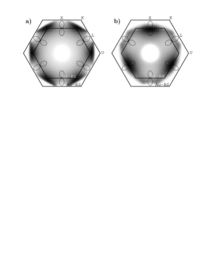
where refers to the metal layer at the interface, and is the Schottky barrier height (assumed to be 0.86 eV); note that the transmission coefficient is zero outside the ellipsoids allowed by energy conservation (see Figure 1). The integral inside the first Brillouin zone is performed summing over a dense grid of special points[15].
In previous publications we have discussed how the propagation of electrons in the gold periodic lattice results in focused beams and narrow Kossel-like lines in real space, with a 3-fold symmetry associated to the direction of an fcc crystal [7, 11, 13]. These lines have typical widths of around 3-4 atomic distances, explaining the nanometric resolution of the BEEM technique even in deeply buried interfaces. These results also show how the Bloch wave is formed after propagation by more than four or five layers, forbidding the propagation of electrons in gap directions over longer distances. We believe that our results are convincing enough to answer a question nowadays found in the literature related to Monte-Carlo simulations: is it realistic to assume that electrons can propagate or Å as free particles along the forbidden Au(111) directions? We conclude that this is an unphysical scenario because of the strong deflection exerted by the lattice on electrons traveling in these directions.
However, in this work we shall focus on our results in reciprocal space and their influence on the I(V) curves. An important feature observed in reciprocal space is a change in the symmetry of the k-space current distributions when going from thin to thick layers. The expected symmetry for a quantum-mechanical calculation is related to the projected density of states[16]. It is six-fold in (111) fcc planes, because of the equal contribution of and states. This is indeed the case for an arbitrarily small imaginary part () added to the energy, but as commented above, can be interpreted in terms of a complex self-energy arising from inelastic events defining a coherence region of the order of . Beyond that region inelastic processes become important, and intensities rather than amplitudes add to give the final wavefield. This takes us from a quantum mechanical picture (six-fold) to a semi-classical one (three-fold), as can be seen comparing Figure 1a, inside the coherence region, to Figure 1b, where the current distribution is computed in a layer outside that area. The three-fold symmetry is progressively built up as a function of metal thickness, and can be understood in terms of our previous analysis[7]: the symmetry of the wavefield in the semiclassical limit is related to the Fermi surface, reflecting the three-fold symmetry of the crystal. Therefore, this is a new example of how a quantum system, under the influence of friction, becomes gradually classical by a decoherence process[17]. In addition, it is seen how the current in k-space deviates for these thick layers from a simple density of states calculation[16], concentrating around the directions predicted by the semiclassical analysis (Figure 1b)[7, 11]. The difference observed in reciprocal space between the quantum and semiclassical regime does not significantly affect

the beams in real space (where the symmetry must always be three-fold), but could in principle affect the I(V) current injected through the projected ellipses into the semiconductor. However, because of the gradual crossover seen from one regime to the other, we do not expect dramatic effects, unless one could experimentally break the time-reversal symmetry suddenly (e.g., by application of a magnetic field), or could selectively block the current injected in some of the six equivalent ellipsoids. In those cases, a sudden jump between a semiclassical regime and a quantum one should be observable. It should be noted that band structure effects results in k-space current with enough to have the electrons injected into the outer conduction-band minima of Si (the central one is forbidden because of the gap in that direction), and explains the long standing puzzle of why the threshold on Au/Si(111) and Au/Si(100) is nearly the same: our calculations show how the similar results obtained for both interfaces are related to these nontrivial distributions in k-space, after the appropriate folding of the gold Brillouin zone inside the silicon one is performed[13].
Next, we compute theoretical I(V) curves from Eq. (2). A quantitative comparison with BEES experiments[18], will then allow us to discuss also the electronic mean free paths. First of all, we try the hypothesis of ballistic electrons. On intuitive grounds this should suffice for low temperature, low voltages, and very thin layers. In Fig. 2 we compare experimental results for Au/Si(111) at T= K, d= Å[18] with a pure ballistic calculation ( very small and injection at first attempt). It is clear from these results that, without using any adjustable parameter, the onset is reasonably explained by a purely ballistic theory that uses the right current distributions in k-space. Therefore, we are able to give a reasonable explanation of the experiment for voltages near the threshold, but it is also noticed in Fig. (2) that data beyond V= eV can only be consistently interpreted by assuming an attenuated wave. To introduce an attenuation mechanism, people have considered three major sources of damping: electron-electron, electron-phonon and electron-defect interaction. As the electron-phonon contributions are greatly reduced at K we first consider a dominated by the electron-electron interaction. Within an RPA approximation for a free electron gas with a density representing gold (), we obtain:
| (5) |
with Å (eV)2. Results considering multiple reflections[18] between the surface and the interface through a specular model are presented in Fig. (2), where an excellent agreement is seen again up to eV. Beyond that voltage, a reduction in the attenuation length by about 20% on average is required to bring experimental and theoretical intensities close together. The resulting is displayed in the inset of Fig. (2). The reduction with respect to the first-principles RPA approximation might be understood as representing either band-structure or impurity effects in the effective electron-electron interaction. It is remarkable the good agreement obtained for low voltages, where the changes quickly with energy following an RPA-like behaviour. This is at variance with E-space Monte-Carlo simulations whereby a smoother dependence of with energy was found [18]. Our results suggest, however, that for thin films and low voltages, the main source of damping is the electron-electron interaction that is well described within a RPA approach.

However, a different example of BEES-data, where a pure ballistic theory is not sufficient even near the threshold, is afforded by the case of thick layers (see Fig. 3). In this case we notice that if we use a RPA-like energy dependence for , we find both a discrepancy in magnitude and a different voltage dependence for I(V) (as seen in the different slopes). If we choose a different in the RPA expression to get the right magnitude, we still would observe a serious discrepancy with the experiment (e.g., see Fig. (3) where has been reduced to Å (eV)2). Because all the other elements in the theory that might be responsible for the discrepancy ( and in formula (4)) are calculated from first principles, we take this as a serious indication of a different dependence of with E. A possible physical origin for this effect is the likely presence of defects (e.g. vacancies)[19]. The natural choice for this scenario is an energy-independent attenuation length in the Green function. With this assumption we obtain an excellent agreement with the experiment ( K, Å[18]) for Å, as seen by the solid line in Fig. 3. This value is in reasonable agreement with attenuation lengths derived by different groups in films of similar thickness[18, 19] and suggests a different behaviour of between thick ( Å) and thin ( Å) films.
In conclusion, we have introduced a Green’s function formalism that in the ballistic limit is an ab initio approach to BEEM. The particular k-space current distributions determined by band structure effects are the main result of our analysis and crucial for a quantitative comparison with experimental BEEM data. Inelastic effects have also been approximately included by use of an imaginary self-energy. This single quantity is fitted to the experiments to explain a number of spectroscopic data on the Au/Si interface.
We acknowledge financial support from the Spanish CICYT under contracts number PBB94-53 and PB92-0168C. K.R. is grateful for financial support from SFB292 (Germany). We are grateful to Prof. K. Heinz for his support.
REFERENCES
- [1] On leave from: Lehrstuhl für Festkörperphysik, University of Erlangen-Nürnberg (Germany)
- [2] W.J. Kaiser and L.D. Bell, Phys. Rev. Lett. 60 1406 (1988); L.D. Bell and W.J. Kaiser, Phys. Rev. Lett. 61 2368 (1988).
- [3] For comprehensive reviews see M. Prietsch, Physics Reports, 253, 164 (1995), and L.D. Bell, W.J. Kaiser, Annu. Rev. Mater. Sci. 26, 189 (1996).
- [4] R. Ludeke, Phys. Rev. Lett. 70, 214 (1993).
- [5] A.M. Milliken, S.J. Manion, W.J. Kaiser, L.D. Bell and M.H. Hecht, Phys. Rev. B 46, 12826 (1992).
- [6] L.J. Schowalter, E.Y. Lee, Phys. Rev. B 43, 9308 (1991).
- [7] F.J. Garcia-Vidal, P.L. de Andres, F. Flores, Phys. Rev. Lett. 76, 807 (1996).
- [8] J.C. Slater and G.F. Koster, Phys. Rev. 94, 1498 (1954).
- [9] D.A. Papaconstantopoulos, Handbook of the band structure of elemental solids (Plenum, New York, 1986).
- [10] L.V. Keldysh, Sov. Phys. JETP 20, 1018 (1965).
- [11] P.L. de Andres, F.J. Garcia-Vidal, D. Sestovic, F. Flores, Phys. Scripta T66, 277 (1996).
- [12] F. Guinea, C. Tejedor, F. Flores and E. Louis, Phys. Rev. B 28, 4397 (1983)
- [13] P.L. de Andres, K. Reuter, F.J. Garcia-Vidal, D. Sestovic and F. Flores, Appl. Surf. Sci. (in press); cond-mat/9710091.
- [14] F. Garcia-Moliner and F. Flores, Introduction to the theory of solid surfaces, Cambridge Univ. Press, 1979 (Cambridge).
- [15] R. Ramirez and M. C. Böhm, Int. J. Quantum Chem., 30, 391 (1986).
- [16] M.D. Stiles and D.R. Hamann, Phys. Rev. Lett. 66, 3179 (1991).
- [17] W. H. Zurek, Physics Today 44, 36 (Oct. 1991).
- [18] L.D. Bell, Phys. Rev. Lett. 77, 3893 (1996).
- [19] C.A. Ventrice Jr., V.P. LaBella, G. Ramaswamy, H.P. Yu, L.J. Schowalter, Phys. Rev. B 53, 3952 (1996).