Observation of Quantum Fluctuations of Charge on a Quantum Dot
Abstract
We have incorporated an aluminum single electron transistor directly into the defining gate structure of a semiconductor quantum dot, permitting precise measurement of the charge in the dot. Voltage biasing a gate draws charge from a reservoir into the dot through a single point contact. The charge in the dot increases continuously for large point contact conductance and in a step-like manner in units of single electrons with the contact nearly closed. We measure the corresponding capacitance lineshapes for the full range of point contact conductances. The lineshapes are described well by perturbation theory and not by theories in which the dot charging energy is altered by the barrier conductance.
pacs:
PACS 73.23.Hk, 73.23.-b, 73.20.Fz, 72.15.RnReceived
In classical physics, a puddle of electrons holds a discrete and measurable number of electrons. Quantum mechanics instead dictates that the probability for an electron to be in a localized state on the puddle depends on the coupling strength to the environment. For many systems in which a single state is coupled to a continuum, this coupling produces a “lifetime broadening” of energy levels. For instance, atomic spectra display a characteristic Lorentzian lineshape broadening [1]. In analogy with atomic spectroscopy, several experiments have demonstrated the capability of precisely measuring the energies to add electrons to quantum dots [2]. In contrast to atomic physics, the lineshape of quantum dot levels originates essentially in a many-body interaction between electrons in the dot and the macroscopic environment.
As the tunnel barrier conductance, , between the quantum dot and the macroscopic leads is increased above , charge is no longer quantized and the Coulomb blockade is destroyed. This process has been attributed to quantum charge fluctuations between the dot and the environment [3]. A thorough physical description of this effect has only been recently proposed in the nearly closed regime [4, 5] and the nearly open regime [6].
Experiments measuring the charge or the capacitance of a dot provide the most direct information about charge fluctuations and the effect of the dot-environment interaction on the charging states of the dot. However, transport measurements have been the first to address the issue of dot-environment coupling. In one of the first studies, Foxman et. al. [7] examined the lineshape of conductance peaks with increasing coupling of the dot to the leads and found good agreement with Lorentzian broadening. To analyze the charging lineshapes in the dot for a broad range of coupling strengths, conductance measurements are poorly suited, being complicated by other processes such as cotunneling [8] and Kondo coupling [9].
Previous experiments have addressed the issue of charging lineshapes. Experimenters employed a semiconductor electrometer [10] to observe the effect of charge fluctuations. They modeled their results by a reduction of the charging energy with increasing coupling. In another experiment, the effect of tunnel barrier conductance on Coulomb blockade was studied through peak splitting of double dots [11]. In this case, the spacing between double-dot peaks can be predicted with a similar formalism as we use in our lineshape analysis [12].
We have developed an experiment which probes the capacitance lineshape of a quantum dot with unprecedented sensitivity. We find that the lineshapes deviate substantially from previously employed fitting forms [7, 10] and are best described for all coupling strengths by the theory developed recently by Matveev [5, 6].
We measure the capacitance lineshapes of a quantum dot with only one contact to a charge reservoir. The quantum dot is electrostatically defined in a two-dimensional electron gas (2DEG) of a AlGaAs/GaAs heterostructure. The 2DEG is about 1200 below the surface with a carrier concentration of cm-2. Measurements were performed on six different samples, each yielding very similar results, and here we present detailed data from one of them. A micrograph of the structure is shown in Fig. 1a. The estimated area of the quantum dot is about 0.5, which corresponds to an energy level spacing of 7eV. We measured the average charging energy of the dot to be meV from temperature dependence of the capacitance peaks for high tunneling barriers. Here, =348aF is the total capacitance of the quantum dot. These parameters agree with what we expect from geometrical considerations.
The charge on the quantum dot is measured with a single-electron transistor (SET) with extremely high sensitivity [13]. The metal SET is fabricated [14] with Al-Al2O3-Al tunnel junctions using the standard shadow-evaporation method [15]. To maximize the sensitivity to the quantum dot charge, we incorporate the SET directly into one of the leads defining the dot.
Figure 1b. shows the drain-source current-voltage relationship of the SET. It changes cyclically with the charge induced on the central island of the SET. The dependence of the current on the SET central island charge is shown in Fig. 1c. For optimal charge sensitivity of the SET, we set the drain-source voltage at the onset of conduction for the maximum Coulomb blockade condition [16], as shown by the arrow in Fig. 1b. For the sample primarily discussed in this Letter, we achieve a sensitivity of to the quantum dot charge.

Through application of a DC voltage, , to the lead marked “gate” in Fig. 1a, charge can be drawn onto the dot as , where is the gate-dot capacitance. However, for zero temperature and for high tunneling barriers separating the dot from the leads, the charge on the quantum dot is quantized and can only change from to around points in gate voltage, where . The measured capacitance is , where is the average number of electrons on the dot.
The capacitance lineshape is measured by applying a small ac excitation (40 V rms, 1kHz) to the gate. This signal modulates the charge on the quantum dot by an amount that is a function of and the coupling strength. The small ac modulation of the quantum dot charge induces ac charge on the SET central island resulting in a current through the SET at the excitation frequency. Examples of measured SET response as is swept are shown in Fig. 2a for three different tunnel coupling strengths. The upper trace is obtained for , where deviates only slightly from and the electrostatic potentials in the dot and the leads are nearly equal. A prominent feature of this curve is an oscillation with a period of 94mV. This period arises due to an addition of one electron to the SET central island through a direct capacitance aF to the gate, modulating the gain of the SET.

The bottom trace in Fig. 2a is obtained for . Here, the charge on the dot is well quantized and can only change in close proximity to points where . These points correspond to the sharp peaks in the trace, spaced with a mean period of 6.3mV, yielding a gate-dot capacitance of . Notice that the large-period background oscillation has a larger amplitude compared with the upper traces in Fig. 2a. Between the peaks, the dot potential is effectively floating; charge cannot enter the dot from the reservoir to screen the ac gate potential. Thus, more charge is induced on the SET in response to the ac excitation on the gate because the ac coupling from the gate to the SET is augmented by a factor of . Here is the quantum dot-SET central island capacitance.
In general, the charge response on the SET central island, , to the ac excitation on the gate, , can be expressed as:
| (1) |
As our SET operates in the linear response regime, the current through the SET directly reflects . Linear response is ensured because the ratio of to the total capacitance of the SET central island is about 0.05. Therefore, a change of charge of one electron in the quantum dot only induces of an electron on the SET. Moreover, we obtain our capacitance lineshapes at maximal gains of SET where this small induced charge has minimal effect on the SET gain. The reverse effect of the SET on the quantum dot charge is also very small. The ratio is approximately 0.06, producing negligible feedback. Also, the charge on the SET central island is poorly quantized since a finite source-drain voltage is applied to the SET. Using equation (1), we extract the quantum dot capacitance lineshapes, , from the raw data as a function of the tunnel barrier conductance.
During the measurement of the capacitance lineshapes, point contact 2 is completely pinched off, and the dot is coupled to the leads only through point contact 1. To determine the conductance of contact 1 in this regime, we perform the following procedure. The conductance of contact 1 is measured with 2 completely open. To account for the electrostatic coupling between contacts 1 and 2, we monitor the shift of conductance plateaus of contact 1 as 2 is being closed. This procedure allows us to extrapolate , the conductance of contact 1, to the regime of the capacitance measurement.
Figure 2b shows the evolution of the capacitance lineshape with increased coupling strength. The nominal values of are: 0.010, 0.67, 1.09, 1.50 and . It is clear that as increases and approaches , the capacitance peaks broaden and the Coulomb blockade oscillations diminish and disappear. Below, we discuss the lineshapes of different quantum dot capacitance peaks in various coupling regimes: very weak, weak and strong.
In the very weak coupling regime, the shape of the capacitance peak is determined simply by thermal broadening. Figure 2b shows good agreement between a peak measured with and a derivative of the Fermi-Dirac function for a temperature of 130mK.
For larger tunnel barrier conductance, the capacitance lineshape changes. In Figs. 3a, b, c and d, we plot with open circles capacitance peaks that we obtained for nominal values of =0.67, 1.09, 1.50 and 1.81. We compared our capacitance peaks with expressions that have been previously used to fit conductance peaks. For example, Lorentzian lifetime broadening has been considered [7] for characterizing the charge smearing effects. In Fig. 3a, the lower plot of Fig. 3b, Figs. 3c and d, we plot Lorentzian-broadened Fermi peaks with energy level widths =0.15, 0.32, 0.44 and 1.0. The lineshapes show significant deviations from the data. To avoid clutter, we have fit the Lorentzians to the valleys between our peaks. Nonetheless, fitting to the peak centers gives an equally poor result.
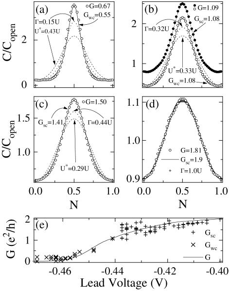
Previous measurements of charge fluctuations used a renormalized charging energy to account for peaks broadened with a finite tunnel barrier conductance [10]. In Figs. 3a, b and c, we plot derivatives of the Fermi function with =0.43, 0.33 and 0.29 for a temperature of 130mK. These lineshapes clearly do not fit the data either.
Finally, we compared our experimental results to the theoretical treatment developed by Matveev [5, 6]. The problem of interaction between the dot and the leads was solved in the limits of weak [4, 5] and strong [6] coupling using either transmission or reflection of the tunnel barrier as a small parameter in perturbation theory. In both limits, the physics of charge fluctuations is related to spin fluctuations in the Kondo problem. Here, instead of the degeneracy of the two-spin states, there is a degeneracy between the dot states with and electrons. Similarly to the Kondo effect, the charge displays a logarithmic divergence around these degeneracy points at very low temperatures. As a result, the predicted capacitance lineshape has more weight around the half integer values of in comparison with other theoretical treatments.
For weak coupling, this effect becomes pronounced at experimentally unattainable temperatures. Therefore, in the range of , it suffices to treat the tunnel coupling between the dot and the leads, , with the lowest orders in the perturbation theory. The expression for the capacitance far from the peak center is [4, 5]:
| (2) |
Near the peak center, the calculation for non-zero temperatures yields an expression with a Fermi-Dirac component and a correction that is linearly dependent on [17]. In the theory [5], .
For strong tunneling, the theory [6] is based on perturbation in the reflection amplitude. Here, the capacitance lineshape is:
| (3) |
The reflection coefficient, , is related to the tunnel barrier conductance as: . is a constant, determined by normalizing the integral of to one electron, . The logarithmic divergence is analogous to a similar behavior of magnetic susceptibility in the two-channel Kondo problem [18]. To account for a finite temperature, the singularity in (3) is cut off by replacing with . The corrected expression was used for the fits.
We fit every measured capacitance peak with the above described expressions using the conductance as a parameter with least squares optimization. In Fig. 3a and the lower plot of Fig. 3b, we show fits for weak tunneling with conductances of and 1.08. These peaks are in excellent agreement with our data measured with tunnel barrier conductances of 0.67 and 1.09, respectively. The strong tunneling lineshapes are shown in the top plot of Fig. 3b and in Figs. 3c and d. These figures show the strong tunneling calculations for conductances of , 1.41 and 1.90. There is excellent agreement of these lineshapes with our data, obtained with conductances of 1.09, 1.50 and 1.81. Both the weak and strong coupling theories fit well to the capacitance lineshape obtained for 1.09, shown in Fig. 3b. Fig. 3d shows a capacitance peak for a nearly transparent tunnel barrier conductance. Here, the lineshape is almost indistinguishable from a sinusoid and it is difficult to discern any significant differences between any of the theoretical calculations.
In the case of weak coupling, we found that on average, corresponds to the experimentally measured value if . For strong coupling, we found that the coefficient , to maintain the dependence of the capacitance lineshape on in this limit. Similar discrepancies were observed elsewhere [19], but their cause is not known at this time.
Figure 3e shows the dependence of the tunnel barrier conductance on the voltage of the lead defining the tunnel barrier. We also plot the conductance values obtained from theoretical fits in the weakly and strongly coupled regimes. These values have large fluctuations around the measured tunnel barrier conductance. These fluctuations are a mystery that remains to be solved. They are seen consistently in all of our samples. Evidently, for a dot with a single point contact, the tunnel barrier conductance affecting the lineshape is different from the conductance through the dot which does not display comparable fluctuations. In gate voltage sweeps for a fixed tunnel barrier conductance, the values of or are correlated over a few adjacent peaks. A similar effect was observed in conductance measurements in dots in the quantum Hall regime [20]. Theorists predict that such fluctuations can arise from quantum interference inside the dot and should therefore be highly sensitive to magnetic field. This is consistent with results from conductance experiments [21]. There are similar theoretical predictions for fluctuations in capacitance peaks [22]. However, we observed no effect of magnetic field for magnetic fluxes through the dot as high as 30 flux quanta.
We thank K. Matveev, L. Levitov, and L. Glazman for numerous helpful discussions. This work is supported by the Office of Naval Research, the National Science Foundation DMR, the David and Lucille Packard Foundation, and the Joint Services Electronics program.
REFERENCES
- [1] V. F. Weisskopf and E. Wigner, Z. Physik 63, 54 (1930).
- [2] R. C. Ashoori, Nature 379, 413 (1996); M. A. Kastner, Physics Today 46, 24 (1993); L. P. Kouwenhoven et al., Science 278, 1788 (1997).
- [3] M. Devoret and H. Grabert, in Single Charge Tunneling, edited by H. Grabert and M. Devoret NATO ASI, Ser. B, 294 (Plenum, New York, 1992).
- [4] L.I. Glazman and K.A. Matveev JETP 71, 1031 (1990).
- [5] K. A. Matveev, Sov. Phys. JETP 72, 892 (1991).
- [6] K. A. Matveev, Phys. Rev. B. 51, 1743 (1995).
- [7] E. B. Foxman et al., Phys. Rev. B 47, 10020 (1993).
- [8] A. Furusaki and K. A. Matveev, Phys. Rev. Lett. 75, 709 (1995).
- [9] D. Golhaber-Gordon et al., Nature 391,156 (1998).
- [10] L. W. Molenkamp, K. Flensberg, and M. Kemerink, Phys. Rev. Lett. 75, 4282 (1995).
- [11] C. Livermore et al., Science 274, 1332 (1996).
- [12] K. A. Matveev, L. I. Glazman and H. U. Baranger, Phys. Rev. B 54, 5637 (1996).
- [13] K. K. Likharev, IEEE Trans. Magn. 23, 1142 (1987).
- [14] D. Berman et al., J. Vac. Sci. Technol. B 15, 2844 (1997).
- [15] T. A. Fulton and G. J. Dolan, Phys. Rev. Lett. 59, 109 (1987).
- [16] P. Lafarge et al., Z. Phys. B. 85, 327 (1991).
- [17] K. A. Matveev, private communication, 1997.
- [18] N. Andrei and C. Destri, Phys. Rev. Lett. 52, 364 (1984).
- [19] D.S. Duncan and R.M. Westervelt, private communication, 1998.
- [20] P.L. McEuen et al., Phys. Rev. Lett. 66, 1926 (1991).
- [21] R.A. Jalabert, A.D. Stone and Y. Alhassid, Phys. Rev. Lett. 68, 3468 (1992); A.M. Chang et al., Phys. Rev. Lett. 76, 1695 (1996); J.A. Folk et al., Phys. Rev. Lett. 76, 1699 (1996).
- [22] I.L. Aleiner and L.I. Glazman, cond-mat/9710195 (to appear in Phys. Rev. B 57, 1998); A. Kaminsky, I.L. Aleiner, and L.I. Glazman, cond-mat/9802159.