[
Tight-binding molecular-dynamics studies of defects and disorder in covalently-bonded materials
Abstract
Tight-binding (TB) molecular dynamics (MD) has emerged as a powerful method for investigating the atomic-scale structure of materials — in particular the interplay between structural and electronic properties — bridging the gap between empirical methods which, while fast and efficient, lack transferability, and ab initio approaches which, because of excessive computational workload, suffer from limitations in size and run times. In this short review article, we examine several recent applications of TBMD in the area of defects in covalently-bonded semiconductors and the amorphous phases of these materials.
Invited review article for Computational Materials Science
]
I Introduction
As one will be able to judge from this special issue of Computational Materials Science, tight-binding (TB) molecular dynamics (MD) has evolved into a powerful method for understanding material properties at the atomic level, offering a good compromise between empirical[3] and first-principles[4] approaches for describing the interactions between atoms. Indeed, empirical methods lack transferability — model potentials are usually fitted to specific material properties in specific configurations, and often fail to properly describe situations and properties other than those on which they were fitted. In contrast, first-principles methods are transferable, but their computational workload is so great that only small systems (less than a hundred particles or so) can be dealt with on relatively short timescales (at most a hundred ps or so) on the fastest computers.
With TBMD, and in particular the novel methods (for a review, see, for instance, Ordejon’s paper in this journal and Ref. [5]), it is possible to simulate systems containing several hundred particles for a good fraction of a ns. This allows a number of interesting problems to be addressed, as we illustrate below. In fact, the accuracy and power of the method can be enhanced considerably by combining it with other approaches, either empirical or first principles; we also give examples of this below.
The purpose of the present review is to illustrate the scope of application of the TBMD method by means of selected examples. TB is a field that has been active for some time in the world of electronic structure calculations[6], but only in recent years has it been coupled to MD, making it possible to study the interplay between structure and physical properties of materials. Thus it is possible, with TBMD, to investigate dynamical properties per se, including relaxation, as well to optimise structural models, after which the electronic and other properties can be determined.
We focus here on covalently-bonded semiconductors, mostly Si and the III-V’s; carbon is the object of another article in this Journal. This review is not meant to be exhaustive — but rather illustrative — and thus necessarily incomplete; we therefore apologize to all whose work is not covered or mentioned. Two classes of problems are examined: first, defects — be they localised or extended — and, second, amorphous covalent semiconductors. TBMD has allowed significant progress to be made in the study of defects: because they are of quantum-mechanical nature, TB potentials are more reliable and more accurate than empirical ones; at the same time, because they are semi-empirical, they allow larger systems to be studied on longer timescales than fully ab initio approaches. The same same applies to the study of amorphous materials, where the principal difficulty is in the proper description of the wide spectrum of highly-strained environments that are found in these materials. Of particular interest is the relation between structural and electronic properties which, evidently, cannot be derived from empirical models. Before discussing these applications, we provide, for completeness, a short overview of the methodology; more details on TBMD can be found in, for instance, Ref. [7], as well as other articles in this issue; an excellent discussion of MD can be found in Ref. [3].
II TBMD
TB is a standard method [6] for computing the electronic properties of materials in terms of a set of parameters describing the overlap between atomic orbitals on nearest-neighbour and, sometimes, second-nearest-neighbour sites. In order to carry out MD or static relaxation calculations (i.e., to compute the forces), however, it is necessary to add to the total energy a repulsive term which includes a position-dependent electronic bonding energy as well as ionic contributions. The total energy for TBMD simulations can thus be written as
where the first term on the right is the “band-structure” energy, i.e., the quantum-mechanical bonding energy resulting from the overlap of atomic orbitals, and the second term is a two-body classical potential which accounts for all the other contributions to the total energy. The electronic eigenvalues are obtained from a simplified local-atomic-orbital representation of the Hamiltonian. The electronic wave-functions are generally expanded in terms of a reduced number of localised, orthonormal basis functions
where the coefficients are obtained by solving
In general, the basis set is restricted to the valence electron states. In the case of silicon, for example, one typically uses the single 3 and the three 3 orbitals — a much smaller basis set than would be needed in a plane-wave description of the electron wavefunctions.
Different potentials differ in the way that the Hamiltonian matrix elements are approximated, but also in the functional form of the two-body potential. The matrix elements — which depend a priori on distance and bond angles — are determined either from ab initio calculations or extracted from experiment. The most common approximation consists in parametrising the overlap integral in terms of a set of constants which decay as , with a cutoff distance between the first and second-neighbour shells; a short cutoff distance speeds up the calculations but can be a source of problems in disordered materials where near-neighbour shells are not perfectly separated. It is also possible to compute the matrix elements and the repulsive potential in a more accurate way using either the local-density approximation [8] or the local-orbital representation of density-functional theory first introduced by Harris[9]. These schemes, often dubbed “ab initio TB”, constitute a trade-off between the accrued computational effort associated with them and the more accurate description of strained environments which is of particular importance for disordered materials and defects.
III Defects
Defects play a major role in determining the physical properties of semiconductors[10]. Even when present at low density, they affect deeply the electronic structure of the materials. This is true of point defects, but also of extended defects, especially in the case of quantum structures. In spite of numerous experimental or theoretical studies, a complete picture of the structure of even the simplest defects (vacancies, interstitials, and small complexes of them, such as divacancies), in the most-studied semiconductor material — silicon — has not yet emerged. Defects, further, are not static objects, and can undergo diffusion at sufficiently high temperature. Again, little is known of such processes; the diffusion coefficient of H in Si, for instance, is still not understood in detail.
TBMD calculations of defects have contributed to our understanding of their static and dynamic properties, but they have also been extremely useful in validating the models. Indeed, because they break the local symmetry, which often results in subtle relaxation and electronic effects, defects are difficult to treat using empirical models and therefore serve as an excellent test of the ability of TB models to deal with low-symmetry situations. The details of the atomic structure of defects, however, are generally not known from experiment, and the tests must be against ab initio calculations, which themselves carry significant uncertainties because of limitations in size and computational load.
Here we examine recents results on intrinsic (or native) defects. Extrinsic defects, i.e., impurities, are a difficult problem because of the additional complexity involved in constructing multi-species interactions. We nevertheless consider some exceptions, notably H diffusion in Si and B relaxation in Si.
A Intrinsic point defects in silicon
1 Basics
One of the first applications of TBMD was the study, by Wang et al.[11], of native point defects in crystalline silicon using the TB model of Goodwin, Skinner and Pettifor (GSP)[12]. Wang et al. have examined the formation energies of neutral monovacancies and self-interstitials as a function of the size of the simulation cell — up to 512 atoms. The results are listed in Table I: One sees that size somewhat influences the formation energy, especially for the monovacancy, indicating that the distortion pattern of the defects cannot be accommodated fully by a small cell. The relaxed values of the formation energies seem to fall close to results obtained in the local-density approximation (LDA) [16, 17, 18], probably within the uncertainties inherent to both approaches.
For the single vacancy, Wang et al. find a tetragonal Jahn-Teller distortion on top of the radial displacement of nearest-neighbour atoms, as was also observed by Song et al.[19]. This agrees with the electron paramagnetic resonance measurements of Watkins[20], as well as the LDA calculations of Baraff et al.[21] and, more recently, Seong and Lewis[18]. The LDA calculations, however, predict slightly larger total displacements than TB — 0.4 versus about 0.3 Å. The Jahn-Teller distortion is of quantum-mechanical origin and therefore not available from empirical models.
Song et al.[19] have used the GSP model to investigate, in addition, the simple and split divacancies, as well as the Frenkel pair, all in their neutral charge states; the results as shown in Table I. The formation energies are large and the relaxation energies — the difference in energy between unrelaxed and relaxed configurations, given in parenthesis in Table I — clearly non-negligible, typically representing a good fraction (30% or so) of the formation energy. Of course, this is accompanied by a significant change in volume during relaxation, and atomic displacements that can be as large as 1.25 Å (in the case of the split divacancy[19]).
Within the GSP-TB model it is energetically favourable for two vacancies to “coalesce”, saving about 1.68 eV in the process. Indeed, the formation energy of two isolated vacancies is 7.36 eV, dropping to 6.54 eV for the split divacancy, and to 5.68 for the simple divacancy. Thus, divacancies are expected to readily form and be relatively stable even at high temperatures. Likewise, the formation of a Frenkel pair by a vacancy and an interstitial can reduce their total energy by as much as 1.43 eV – from 7.98 to 5.55 eV.
The activation energy for diffusion is the sum of formation and migration energies. The latter is the energy at the transition state between two equilibrium sites. Song et al.[19] estimate the migration energy for the vacancy to be less than 1.0 eV so the activation energy, using the formation energy values discussed previously, must be less than 4.7 eV. Likewise, tetrahedral interstitials migrate via hexagonal sites with an energy of about 0.63 eV, and thus the activation energy in this case would be of the order of 5.0 eV.
As mentioned above, the atomic displacements for the monovacancy are predicted by the LDA to be slightly larger than the TB values. The opposite is true in the case of divacancies, where the LDA predicts displacements substantially smaller than the TB model of GSP[18]. The LDA, further, leads to a resonant-bond Jahn-Teller distortion (as opposed to the usual pairing configuration) for the simple divacancy that is not observed in TB calculations. Also, the relaxation energies obtained from the GSP-TB model for the divacancies are significantly larger than the corresponding LDA values.
The formation volumes of the vacancy and the interstitial have been calculated by Tang et al.[22] using the TB model of Kwon et al.[14]. The formation volume is defined as , where is the relaxation volume associated with the defect (i.e., arising from the relaxation of the atoms in the neighbourhood of the defect) and is the volume per atom of the perfect crystal; the plus sign is for vacancies while the minus sign applies to interstitials. Using a 216-atom supercell, and after a careful search for the equilibrium volume of the perfect crystal, Tang et al. obtained a relative formation volume of 3% (contraction) for the vacancy and 10% (expansion) for the interstitial. Thus, the volume changes arising from the presence of these defects should cancel each other to a large extent, in agreement with diffuse x-ray scattering experiments[23].
Though the picture is far from being complete, and it is therefore difficult to draw meaningful conclusions on the accuracy of the TB models, it seems to be the case that the model of Kwon et al.[14] overestimates the relaxation energies, while that of Lenosky et al.[15] appears to be doing better (at least for the monovacancy). Bernstein and Kaxiras[24] have observed that the agreement between TB and LDA defect formation energies can be improved significantly by relaxing the constraint on the band gap, which is then allowed to vary in the fitting process. Clearly, more precise TB models are necessary in order to capture the subtle details of such low-symmetry situations. Also, more (and better-converged) first-principles calculations are needed to provide a proper reference database for comparison.
Rasband et al.[25] have studied the convergence of intrinsic defect formation energies with respect to potential cutoff distance as well as number of points used to sample the Brillouin zone. Considering isolated vacancies as a test case, they found these variables to affect only very slightly the unrelaxed formation energy, while the effect of relaxation can be sizable. For instance, increasing the cutoff from 3.2 Å (between first and second neighbours) to 4.1 Å (between third and fourth) and using 40 k points rather than one causes the vacancy formation energy to decrease from 3.67 (cf. Table I) to 3.15 eV. The corresponding values for the , and charge states of the vacancy are 2.9, 3.6 and 4.1 eV, respectively. The vacancy is nowhere in the gap a favourable state of the defect, and thus gives rise to the so-called “negative-” effect, that is an effective correlation energy between electrons which is negative[26] (see also below for GaAs).
For the tetrahedral interstitial in its neutral state, now, Rasband et al.[25, 27] find a formation energy of 4.7 eV, using a 4.1 Å cutoff and 40 k points. This is comparable to the 4.40 eV value given in Table I (3.2 Å cutoff, -point only). In the , , , and charge states, the corresponding numbers are 5.5, 4.2, 3.5, and 4.1 eV, respectively, taking the Fermi level in the middle of the gap. Thus, interstitials should occur with a much larger probability than other charge states. This prediction of the stability of the interstitial is in agreement with earlier ab initio results and might explain the discrepancy between experiment (or more precisely “model-fitted” experimental data — cf. Fig. 2 in Ref. [27]) and many calculations. In particular, this result is consistent with metal in-diffusion experiments (see [27] for references).
Rasband et al.[27] have used TBMD to search for new defect structures (interstitials) and have found a whole family of them. For the neutral single interstitial, three stable configurations are found, viz. the T interstitial (formation energy of 4.7 eV), the 110-split interstitial (5.0 eV) and the 100-split interstitial (5.4 eV). The corresponding ionised defects with charges between and range in energy from 5.0 to 6.3 eV for the 110 split, and from 4.5 to 6.3 for the 100 split. As we have seen above, the doubly-ionised T interstitial has a formation energy of 3.5 eV and is thus much more stable than any of the split interstitials. Di-interstitials were also examined. Rasband et al.[27] found a novel low-energy configuration — the “split triple” interstitial, consisting of three Si atoms sharing one lattice site and forming an equilateral triangle in a (111) plane. The formation energy of this defect is a small 3.65 eV per atom in the neutral state, dropping to 3.0 eV in the state. A similar 110 split-triple interstitial has a 3.3 eV formation energy, while a “Z” configuration has 3.4 eV, both in their state, which is the most stable. There is, to our knowledge, no evidence that these objects have been observed experimentally, nor are there other calculations to compare with. In view of the approximate character of TB, the stability of such defects should probably be considered as somewhat speculative at this point.
2 Energy levels
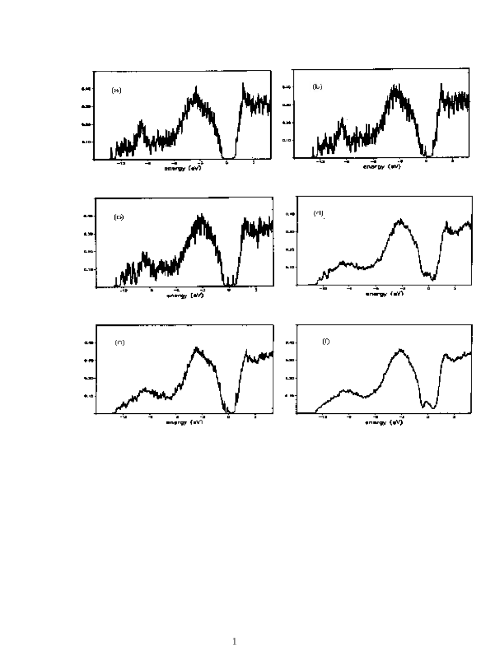
One advantage of TB over empirical approaches is that it gives access to the electronic structure of the material. The GSP model does not provide a very good description of the band structure of Si. It is nevertheless informative to examine, within this model, the effect on the electronic properties of the presence of defects. Fig. 1 shows the density of states near the band gap for the various defect types considered by Song et al.[19]. Defects, evidently give rise to localised bands in the gap. Table II lists the positions of the levels associated with the defects in their relaxed configurations.
The LDA results quoted in Table II are those of Ref. [18], where other references can also be found; however, only very few calculations of the defect levels have been reported. For the monovacancy, for instance, the LDA value for the highest occupied level, 0.23 eV, is in rough agreement with the self-consistent-field calculations of Lipari et al.[28], which gives a singlet level at 0.3 eV (but relaxation was not taken fully into account). Both calculations however disagree with the TB result. For the divacancies, the error bar on the LDA calculation (about 0.1 eV) is such that it is not clear that this defect leads to levels in the gap, in apparent disagreement with the TB results. It should be said, as discussed in Ref. [18], that the precise positions of defect-induced gap levels are rather sensitive to the details of the computational model. All calculations, however, point to the fact that defect levels move towards the valence-band maximum upon relaxing the structure.
Electron paramagnetic resonance (EPR) experiments gives information about the energy levels of charged defects. The and charged states of the vacancy lie close to the top of the valence band, at 0.05 and 0.13 eV, respectively, whereas the and lie at 0.57 eV and 0.11 eV below the bottom of the conduction band. The TBMD results of Rasband et al. are in error with experiment by 0.04, 0.07, 0.17, and 0.90 eV, respectively (see [25] for experimental references). Except for the defect, the agreement can be considered as good.
3 Vacancy clusters in silicon
Structural evolution during non-equilibrium processes such as irradiation and growth is mediated, to a large extent, by the presence of defects or clusters of them. Vacancies, for instance, may coalesce and give rise to microdefects such as voids, bubbles, or dislocations. It is therefore important to have some idea of the structure and energetics of such imperfections.
The case of vacancy clusters has been examined by Bongiorno, Colombo, and Diaz de la Rubia[29] (BCDR) using TBMD. This work was motivated to a large extent by serious disagreements between model potential (Stillinger-Weber) and first-principles studies with regards, in particular, to the shape and energetics of stable clusters. In order to perform these calculations, BCDR exploited the power of the Goedecker-Colombo linear scaling scheme[30] as implemented on a (parallel) Cray T3E. This allowed very large simulation cells to be considered — 1000 atoms — containing vacancy clusters varying in size between 1 and 35. In all cases, the lowest-energy configurations was obtained through a careful relaxation.
BCDR examined two different cluster shapes: spheroidal clusters (SPC), where vacancies are created by simply removing atoms from successive radial shells about a single vacancy, and “hexagonal ring clusters” (HRC), where Si atoms are removed following a ring pattern in the crystal. These structures evidently are different from the geometric viewpoint, but also from the “chemical” viewpoint. Indeed, for a given cluster size, SPC structures have more dangling bonds than HRC structures, as demonstrated in the top panel of Fig. 2, and SPC are therefore expected to be less favourable than HRC because dangling bonds are expensive. This is in fact confirmed by the formation energy, middle panel in Fig. 2, at least for clusters containing 1–24 atoms. For larger clusters, the aggregation path is likely very complex and probably depends on the details of the kinetics of the non-equilibrium process (irradiation or growth).
The binding energy for the various clusters is given in the bottom panel of Fig. 2; there are clearly some “magic clusters”, i.e., clusters who are much more stable than others slightly different in size. This is the case, for instance, of HRC clusters with , 8, 10, 12, 14, 16, 18, etc.; these magic clusters are the result of minimising the number of dangling bonds as as well as structural rearrangements (internal reconstructions).
B Impurity levels in Si and GaP
As we have seen, relaxation affects strongly the structure and energetics of intrinsic defects in semiconductors. This is true also of impurities. The deep levels associated with several impurities in Si and GaP have been investigated using TBMD by Li and Myles[31]. Their approach is based on the theory of Hjalmarson et al.[32] of deep levels, augmented to include lattice relaxation by adding a repulsive pair potential derived from Harrison’s overlap interactions[33]. The host material is described using the TB model of Vogl et al.[34]. The relaxation is performed via MD, but restricted to nearest neighbours and symmetry-conserving displacements, i.e., breathing modes. Full details of the method can be found in Ref. [31].
Table III gives the energies of several deep-level impurities in Si and GaP as calculated by Li and Myles[31]. These are of (as well as ) symmetry, i.e., -like. Also given in Table III are values from experiment (see [31] for references) and the results from the Hjalmarson et al.’s theory[32], which does not include relaxation. Clearly, relaxation is sizable in all cases and improves quite significantly the agreement with experiment. Relaxation proceeds inwards in all cases except GaP:O. Li and Myles indicate that inclusion of second-neighbour relaxation changes the results very little.
C Boron in silicon
Boron is a dopant which is routinely used in the semiconductor fabrication process and it is therefore important to understand at the fundamental level how the host material is affected by the impurity, and how the latter diffuses. As a first step in this direction, Rasband et al.[25, 27] have used TBMD to study defect-dopant pairs as well as boron interstitials in silicon. For Si-Si interactions, the GSP model was employed. For Si-B interactions, a new model à la GSP was developed, with the parameters determined by fitting to ab initio band-structure energies for zinc-blende SiB; full details can be found in Ref. [25].
The TBMD results are found to be generally in good agreement with the ab initio calculations of Nichols et al.[35]. For the boron T interstitial, the TB model gives a formation energy of 3.7 eV, compared to 3.9 eV from first principles. For the neutral boron-substitutional–vacancy complex, Rasband et al. find 2.9 eV compared to 3.0 for Nichols et al.; the binding energy of this complex is 0.39 eV, which compares well to 0.5 ab initio. The binding energy of the boron-substitutional–interstitial complex is 1.2 eV from TBMD, in line with model-fitted data, 1.5 eV. Relaxation of the four Si atoms near a B substitutional impurity is found to be small — about 0.04 Å, independent of the state of charge.
Rasband et al.[27] have looked for “new” defects involving boron. Starting with a boron atom in a T-interstitial position with charge states in the range to , they identified a series of seven different interstitial species having formation energies, in their most stable charge states, between 3.1 and 5.5 eV. They also examined the case where the starting structure was a combination of Si 110-split interstitial adjacent to a B T-interstitial; the resulting configuration after relaxation was a 110-split di-interstitial with a formation energy of 2.5 eV per atom. Further, they observed the formation of a “ring” di-interstitial having a formation energy of 3.1 eV per atom exhibiting a distinctive five-membered ring.
The above results, just as was the case for native defects in silicon, indicate that new elements must be taken into account when experimental defect concentration data are analysed. In particular, assumptions regarding the prevailing charge state of any particular defect should probably be re-examined at the light of the above (and other) results.
D Point defects in GaAs
In the above study of impurity levels in Si and GaP, Section B, relaxation was restricted to radial displacements. While such distortions might constitute the most important component of relaxation, it may be expected that, quite generally, the symmetry is broken by the presence of defects, and this can only be revealed through full relaxation of the lattice.
A TBMD investigation of defect relaxation and energetics in GaAs has been proposed by Seong and Lewis[36]. The study is based on the model of Molteni, Colombo, and Miglio[37], which takes charge-transfer effects into account through a screened, and thus short-range, Coulomb term. Native point defects in GaAs play an important role; this is true, in particular, of the so-called “EL2” defect, which can compensate residual acceptor impurities and pin the Fermi level at midgap, so that GaAs can be manufactured without intentional impurity doping. This defect is thought to be related to the As antisite (substitution of a Ga by an As).
For tetragonally-distorted configurations, it is convenient to describe the relaxation in terms of three displacement components[10, 38]: the “breathing” (radial) mode, and two “pairing” modes, which measure the lateral displacements of the ions (i.e., perpendicular to the breathing mode). Table IV gives the breathing-mode displacements for Ga and As vacancies and antisites in various states of charge. The pairing modes are negligibly small for Ga vacancies and As antisites, but are sizable for As vacancies and Ga antisites; they are given in Table V.
Ga vacancies are found to relax inwards by an amount which is independent of the state of charge, leading to an open-volume contraction of about 34%, consistent with positron lifetime measurements[39, 40], as well as first-principles calculations[38], though relaxation in the latter case is substantially smaller and the position of the corresponding localised states different. The relaxation of As antisites also is the same for all charge states; it is small and, in contrast to Ga vacancies, proceeds outwards, leading to a volume expansion of about 7.5%. This is also what is found in first-principles calculations[41, 42, 43] and experiment[44]. We find the localised state for this defect to lie 0.49 eV above the valence band maximum, in accord with tunneling spectroscopy measurements[44].
Both As vacancies and Ga antisites undergo tetrahedral-symmetry-breaking distortions, i.e., have non-zero pairing displacements. In both cases, further, the relaxation pattern depends sensitively on the state of charge, as can be seen in Tables IV and V. For As vacancies, changes in the open volume range from a 54% expansion in the state to a small 3% contraction in the state. The positron lifetime is therefore expected to be longest in the state and shortest in the state; this is consistent with experiment, which finds a decrease from 295 to 258 ps when the charge changes from neutral to singly negative[39]. In the case of Ga antisites, the changes in the open volume vary between +50% and a negligible 1%; the latter is for the doubly charged vacancy and corresponds, approximately, to the GaAs crystal in its “normal” state. (An As with five valence e- is replaced by a Ga with three e-, then two electrons are added to it).
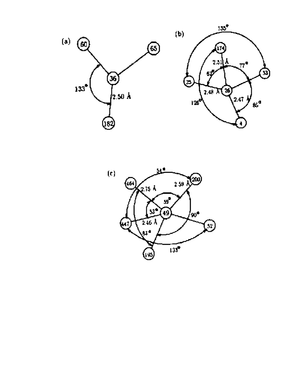
It is of interest to examine more closely the structure of the Ga antisite. The singly-negative Ga antisite undergoes a small (2%) outward breathing-mode displacement, and similar pairing-mode relaxations of the nearest neighbours. The antisite itself is displaced slightly from its ideal lattice position [by about 0.1 Å in the direction]. The distance between the antisite and one of its Ga neighbours (referred to as “Ga1” by Zhang and Chadi[45]) is 2.65 Å, a little bit longer than the equilibrium bond length (2.45 Å). The distance between the Ga antisite and the three other Ga neighbours, which relax very little, is 2.44 Å. This atomic structure near Ga is very similar to that of Zhang and Chadi[45] who studied the problem from first principles; the configuration is depicted in Fig. 3(a). The relaxed state of the neutral Ga antisite is shown in Fig. 3(b). The defect moves away by 0.4 Å from its equilibrium position; the Ga1 atom also moves away, but in the opposite direction, by 0.48 Å. This leads to a “broken-bond” configuration with a relaxed Ga–Ga1 distance of 3.32 Å, in perfect agreement with Zhang and Chadi’s calculation[45]. Positively-charged Ga antisites show similar relaxations.
The variation with electron chemical potential (, where and is the width of the gap) of the formation energy of a given defect in various states of charge provides information about its ionisation level and most stable state. This is displayed in Fig. 4 for the four types of defects considered. A detailed discussion of these results can be found in [36]. The formation energy also depends, however, on the atomic environment that prevails during growth, i.e., on atomic chemical potentials. Fig. 5 shows, for three different values of , the defects of lowest energy as a function of the deviation from the bulk value. At both the valence-band maximum (VBM) and midgap, the As antisite is the most favourable defect in the As-rich limit, while the Ga antisite is the one preferred in the Ga-rich limit. In the middle of the range, the vacancies and take over at midgap, though, in only a narrow window of values. At the conduction-band maximum (CBM), now, dominates in As-rich conditions, while Ga is favoured in the Ga-rich limit. Thus, overall and by in large, antisites have the lowest energies, and these defects are expected to be much more prevalent than vacancies in GaAs. This is consistent with the current interpretation[41, 46, 47, 48, 49, 50] of the EL2 defect being a neutral As antisite with tetrahedral symmetry.
E Dynamics and kinetics of point defects
1 Vacancy and interstitial diffusion and recombination
Vacancies and interstials (as well as small complexes of them and impurities) contribute strongly to the transport of mass in crystalline solids. Yet, little is known on their equilibrium concentrations and diffusivities. The values from experiment vary widely, and it is not clear which of vacancies or interstials dominate transport at a given temperature. Further, the recombination process of the two species is not well understood, and in particular it is not clear whether or not there exists an energy barrier against the recombination. These questions have been addressed, in part, using MD and empirical potentials (e.g., Stillinger-Weber [51]); such calculations however cannot account for the subtle quantum-mechanical details of the process. First-principles methods, on the other hand, are hampered by limitations in size and time that make the study of such problems almost impossible at this time. TBMD offers a good compromise between the two, and was used by Tang et al. to study vacancy and interstitial diffusion and recombination[22]. For this problem, they employed the TBMD model of Kwon et al.[14], which appears to be more accurate than the GSP model insofar as the properties of point defects are concerned for a 216-atom model. The diffusivity calculations were however performed on a 64-atom (plus or minus one) system, running for as long as 200 ps.
The diffusion constant is given by the product of diffusivity and equilibrium concentration, , where
and
is the migration energy and is the formation energy. If the entropy of formation, , is assumed to be independent of temperature, then the diffusion constant takes the Arrhenius form:
where and . is indeed observed in crystalline silicon to be Arrhenius over a wide range of temperatures. The precise values of the prefactor and activation energy for the individual species are still a matter of discussion, but the following values have recently been given by Gösele et al.[52]: eV (vacancies), eV (interstitials), and .
The diffusivities of vacancies and interstitials were simulated explicitly by Tang et al.[22] using TBMD. The migration energies were found to be eV and eV. In this model, the formation energies are eV and eV, leading to activation barriers of and eV, in remarkable agreement with the experimental values quoted above. Tang et al. did not calculate the entropies of formation — this is a very difficult calculation — but have fitted them to first-principles calculations and experiment; they obtain and . The resulting prefactors are cm2/s and cm2/s, i.e., , again in agreement with experiment. Arrhenius plots of the diffusion constants are given in Fig. 6. Diffusion is dominated by vacancies at low temperature. At high temperature, above 1080 ∘C, in spite of a sizeably larger migration barrier, interstitials take over. This crossover effect is due to the relative values of the prefactors — is four orders of magnitude larger than — and find it’s origin in the Meyer-Neldel (compensation) law, which states that, for a family of activated processes, the prefactor increases exponentially with the activation barrier. The validity (and origin) of the Meyer-Neldel law was established in the case of surface diffusion by Boisvert et al.[53].
Mass transport, as noted above, will evidently be affected by the rate at which vacancies and interstitials recombine, which itself depends on the existence or not of a recombination barrier. Tang et al.[22] have used TBMD to investigate this problem. Starting with an interstitial-vacancy pair with the two defects separated by some distance — between two and six nearest-neighbour spacings — MD simulations were carried out at finite temperature in order to follow the migration path and eventual recombination of the defects. The latter does not always take place. For instance, using as initial configuration a dumbbell interstitial and a vacancy three nearest-neighbour spacings away, Tang et al. found that recombination did not occur at 300 K: thermal activity at this temperature is not large enough to overcome the local distortions around the dumbbell induced by the close approach of the vacancy, at least on the timescale of the simulations. Instead, an “I-V complex” forms; the quenched-in state of the complex, which has a formation energy of 3.51 eV, is shown in Fig. 7(a). At elevated temperature, however, the I-V complex annihilates. This is shown in Fig. 7(b)-(e). The annihilation path is found to be a bond-switching process and takes place in about 10 ps at 1500 K; the activation (migration) barrier for the process is about 1.23 eV. The lifetime of the complex is roughly given by ; taking as the Debye frequency, Hz, one finds to be of the order of hours at room temperature, but only a few microseconds at typical annealing temperatures (i.e., 700-800 K or so). The recombination of vacancy-interstitial pairs, in particular with regards to the electronic structure, was examined by Cargnoni et al.[54, 55] by a combination of TBMD and ab initio Hartree-Fock calculations.
2 Hydrogen diffusion in silicon
Because it may form complexes with a variety of intrinsic or extrinsic defects, hydrogen in semiconductors affect deeply their optical and electronic properties. It is usually present as a result of the complicated fabrication process, but is also often intentionally included in order to passivate defects (e.g., unsaturated, or “dangling”, bonds). Being a light species, hydrogen diffuses readily, inducing additional defects along the way and thus affecting the transport properties of the material to an extent which is determined by its relative concentration. It is therefore important to understand diffusion at the atomic level in order to gain better control on the properties of semiconductors.
The rate of diffusion of hydrogen in crystalline silicon remains a matter of debate in spite of the simplicity of the structure of the host material. At low temperatures (below 800 K), the experimental values that have been reported in the literature vary widely, sometimes by as much as two orders of magnitude at a given temperature (see, e.g., [56] for references) . There are very few data available at high temperatures (above 1000 K), but they are in reasonable agreement with the ab initio MD simulations of Buda et al.[57] for H+ (proton) diffusion. Unfortunately, because the timescale for diffusion increases exponentially with temperature, ab initio simulations cannot be carried out at lower temperatures and there exists no empirical model that can deal with this system in a sufficiently accurate way.
The problem of hydrogen diffusion in silicon was addressed using TBMD by Panzarini and Colombo (PC)[56] as well as by Boucher and DeLeo (BDL)[58]. This constitutes an interesting application of the method as it extends quite significantly the range of temperatures that were covered by the ab initio simulations of Buda et al.[57] while accounting, still, for the quantum-mechanical nature of the system. For Si–Si interactions, both used the GSP model; for other interactions, the appropriate parameters were determined by fitting to selected properties of the silane (SiH4) molecule.
Both models give the bond-center (BC) site as the equilibrium site in static conditions (i.e., at 0 K), in agreement with electron paramagnetic resonance [59] and muon spin resonance experiments [60], as well as previous first-principles calculations (see, e.g., [57]). In the BDL model, this accord is obtained at the expense of a phenomenological parameter that accounts for differences in environment between silane and crystalline Si. Other equilibrium sites, almost degenerate in energy (differences of less than 0.1 eV) with the BC site, are also found. PC, for instance, find the hexagonal interstitial site to be very close in energy to the BC site. Both calculations predict that when H sits in the BC position, nearby Si atoms relax by about 0.4 Å, while very little relaxation is observed when H is in the hexagonal site; this agrees with first-principles calculations.
The diffusion path is also subject to debate. Though experiment and theory agree that the lowest energy site is the BC site, the energy of nearby metastable sites — which likely play an important role in diffusion — is not known precisely. Details of the diffusion path, further, are expected to be strongly affected by dynamical effects because the heavy Si atoms cannot follow adiabatically the motion of the lighter H atom. The ab initio simulations of Buda et al.[57], which cover a timescale of about 4 ps, suggest that diffusion consists of a series of hops between highly-symmetric interstitial sites, but other possibilities can also be envisaged.
Both PC and BDL carried out their TBMD simulations for a single H in a 64-atom c-Si supercell. The simulations by BDL cover the temperature range 1050–2000 K, and run for a maximum of 42 ps, while PC examined temperatures in the range 800–1800 K, running their simulations for as long as 300 ps at the lowest temperatures.
Fig. 8 presents the results of several measurements of the diffusion constant, plotted in the manner of Arrhenius. Also indicated on this plot are the ab initio MD data points of Buda et al.[57]; they are found to agree (at least qualitatively) with the high-temperature experimental points of Van Wieringen and Warmholtz, which can be fitted to an Arrhenius law, , with cm2/s and eV. When extended to low temperatures (dashed line in Fig. 8), one clearly sees the deviations from the Arrhenius behaviour; it should be said, however, that there is no “guarantee” that diffusion should be Arrhenius over the whole range of temperatures.
The TBMD data of PC are also indicated in Fig. 8. The agreement with experiment is clearly excellent in the high temperature limit. The data of BDL are not plotted in this figure, but they are found to be extremely well fitted by the Arrhenius law with cm2/s and eV all the way down to 1050 K. This is in striking agreement with experiment, as can be judged by the close similarity between the prefactors and energy barriers. (The differences are unsignificant). PC however observe deviations from Arrhenius already at 1200 K. The reason for this minor discrepancy with the BDL data can perhaps be traced down to statistics. Indeed, 300 ps remains relatively short on diffusion timescales. For instance, for a diffusion constant of cm2/s, a quick calculation indicates that the average distance visited by a diffusing particle would be about 4 Å. This might explain, in part, the deviations that are seen at even lower temperatures; clearly, however, the TBMD data are consistent with the low-temperature behaviour seen in experiment. Further calculations are evidently necessary to reconcile theory and experiment at low temperatures.
Detailed analysis of the trajectories of individual atoms makes it possible to elucidate the mechanism for diffusion. Fig. 9 shows the diffusion path of the H atom over a 25-ps period at 1200 K as calculated by PC; BDL obtain very similar results. The H atom diffuses preferentially via a sequence of jumps from one BC site to another, spending very little time in between; this corresponds to a low-memory, high-friction regime, where the directions of consecutive jumps are uncorrelated. It is found, further, that the H atoms avoids the low charge-density regions, which is inconsistent with the observations of Buda et al.[57] for the diffusion of H+. Both PC and BDL find a correlation between diffusion events (jumps) and the vibrations of nearby Si atoms: At low temperature (less than 850 K or so), the Si–Si stretching mode (65 meV) is not thermally excited, and diffusion becomes difficult because the BC site is an equilibrium site for hydrogen. At these temperatures, further, long jumps (i.e., to sites more distant than near-neighbours) are quenched in.
IV Disordered phases
As already noted in the Introduction, disordered materials — covalently-bonded semiconductors and chalcogenides — is another area where TBMD simulations have provided important new insights, in particular with regards to the interplay between structure and electronic properties.
Many empirical potentials have been developed that give a reasonable description of the liquid and crystalline phases of semiconductors, as well as, for some, clusters; this is the case for instance of the models of Stillinger and Weber[51], Tersoff[61], Biswas and Hamann[62] and, recently proposed, Bazant et al.[63] These models however lack the generality to account for the large variety of highly strained environments — caused by elastic, topological or chemical disorder — that are encountered in amorphous materials. Thus, for instance, the Stillinger-Weber potential fails to reproduce the clean separation observed experimentally between first and second neighbour peaks in the radial distribution function. The problem is particularly serious for materials such as amorphous carbon, where atoms can be found in several different bonding states, or compound materials, where bonding is partly ionic and the nature of the chemical environment plays an important role. There exists, for example, no satisfactory empirical potential for the III-V amorphous compounds.
The availability of accurate potentials is a necessary, but not sufficient, condition for constructing structurally sound amorphous models. The “preparation” algorithm must be capable of finding a reasonable ground state — one in which the number of topological and electronic defects is a minimum — i.e., relaxation must be as exhaustive as possible. Unfortunately, this is more difficult with TB than empirical potentials.
The strong intermediate range disorder found in amorphous semiconductors poses an additional challenge for the development of semi-empirical TB potentials. As for the liquid phase, near-neighbour shells are often ill-defined: The first and second neighbour shells can be blurred either through disorder or simply large mismatch, as is the case for InP, for example. Attention must therefore be given to the radial behaviour of the empirical repulsive potential as well as the cutoff of the matrix element interactions. In spite of these concerns, current semi-empirical potentials, even though often fairly short-range, yield good agreement with experiment. Moreover, ab initio TB interactions, which normally include longer-range interactions, are not affected by this situation.
The first amorphous materials to be studied with TBMD were the elemental semiconductors silicon and carbon. Silicon, which has a well-defined bonding, is a relatively straightforward choice; TBMD a-Si models are discussed in the next section. Carbon, on the other hand, is much more difficult because of the added difficulty associated with its many bonding states; another article in this special issue is dedicated to a-C and we therefore do not discuss it in any detail here but just give, for completeness, a brief overview of work on this material.
Hydrogenation of amorphous semiconductors reduces significantly the strain and greatly improves the electronic properties by removing deep states in the gap. This is particularly so for a-Si, which requires considerable amounts of H to achieve device-quality electronic properties. TBMD simulations have been run to study its effect on structural and electronic properties, in spite of problems associated with its small mass and high diffusivity. Likewise, TBMD has been used to investigate compounds (mostly binaries) — GeSe2, GaN, GaAs — where additional complications arise from partly ionic interactions.
A Elemental semiconductors
1 Amorphous silicon
Silicon is the material of reference in the study of amorphous semiconductors and has been simulated numerically using a variety of techniques. It is widely accepted as a realisation of Polk’s idealised continuous random network (CRN) [64], which regards the material as a collage of randomly-oriented, corner-sharing tetrahedra, thus possessing perfect coordination. Algorithms have been devised for constructing Polk-type CRN’s on the computer, and these will serve as a reference for simulations based on total-energy minimisation such as TBMD.
As noted earlier, amorphous samples can be prepared in the computer in many different ways. Quenching from the melt and annealing is a popular method because it is akin to the real fabrication process. Quench rates for computer models (in particular TBMD) are however many orders of magnitude larger than real ones and the main difficulty therefore resides in cooling slowly enough for the system to be able to find a reasonable low-energy state. Monte-Carlo methods such as the Wooten-Winer-Weaire bond-exchange algorithm[65, 66] and the activation-relaxation technique of Barkema and Mousseau[67, 68], can yield lower-energy configurations, but at the expense of a heavier computational effort unless they are conducted, in part, using empirical potentials.
Kim and Lee[69] (KL) have used TBMD (with the GSP model) and the melt-and-quench approach to construct a 64-atom model for a-Si. The liquid was produced by running at high temperature (1750 K) for 8 ps. (The liquid phase itself is much better described by the GSP TB interaction than by the SW potential; in particular, the number of nearest neighbours and the angular distributions are in close agreement with the values obtained from ab initio MD[70, 72]). The cell was then cooled at a rate which amounts to K/s. The simulations were done in the microcanonical ensemble at the density of the liquid, about 10% larger than that of the crystal, which is itself 1.6% denser than the amorphous phase [73]. Thus, the final amorphous phase is under high compressive strain. The structural properties of the resulting structure are given in Table VI, where they are also compared with the predictions of other models discussed below. The total coordination number, 4.28, is large, a consequence of the excessive cooling rate but also of the compressive strain on the system which severly hampers relaxation in view of the short period of time covered by the simulation. The model displays a rather clean separation between first- and second-neighbour shells despite an unrealistically large number of defect states (floating bonds) in the electronic bandgap, mostly due to the strain associated with overcoordination.
Servalli and Colombo [74] have studied the influence of the cooling rate on the structure the material. They considered a 64-atom system, first ran for 27 ps in the liquid phase, then cooled at rates in the range K/s — that is up to 100 times slower than in KL’s simulations. The volume was varied linearly with temperature between values appropriate for the liquid and amorphous phases. Overall, the coordination is in much better agreement with experiment than KL’s model. Moreover, there appears to be a strong correlation between the cooling rate and the “quality” of the sample. From visual inspection of the data plotted in the original article, the bond angle distribution, in particular, decreases by about 20% between fastest and slowest cooling rate, coming quite close in the latter case to experimental values. Even the slowest rate, however, might not be sufficient for proper relaxation: In one run, for instance, a “major” relaxation event was observed after about 57 ps, indicating that the relaxation time is much longer than a few phononic periods even in such small systems. Servalli and Colombo also prepared a 216-atom a-Si model [74] which, because of computational limitations, was quenched-in over a fairly short time of 11.4 ps. In spite of this, the electronic density of states is comparable to that obtained from a smaller system relaxed for a longer time, suggesting that the size of the unit cell might be an important factor in the total stress found in computer-generated samples.
In order to minimise the computational workload imposed by the long quenching process, mixed approaches, using empirical potentials for the time-consuming preparation followed by TBMD relaxation, can also be used. Mousseau and Lewis[75, 76], for example, have combined TBMD with an efficient optimisation scheme based on classical potentials. A “rough” 216-atom model was first prepared from a randomly-packed configuration using the activation-relaxation technique[67, 68] together with a Stillinger-Weber-type potential. The resulting structure was then relaxed using TBMD and the GSP potential. The final TBMD stage ensures that the model is physically realistic; the initial empirical-potential relaxation is therefore, to some extent, artificial — as is also the case of the Wooten-Weiner-Weaire bond-switching process — but ensures, when combined with such a powerful optimisation scheme as the activation-relaxation technique, that the structural model is fully optimised. This is actually demonstrated in Table VI: the average coordination number is very close to four (but slightly below), as expected, and perhaps more significant, the width of the bond angle distribution is much smaller than obtained in any other model.
An alternative approach was proposed by Drabold et al.[77]; it consists in “incompletely melting” the sample before cooling. This is achieved by introducing a vacancy, which destabilizes the lattice: because the system is small (about 64 atoms in this case), the melting temperature decreases markedly and relaxation proceeds more easily. After a short microcanonical run at high temperature, the system is taken down to zero temperature and relaxed; the calculations were performed using the Sankey-Drabold “ab initio TB” scheme [78]. Although this technique allows for a rapid production of samples, it does not seem at present to be able to yield quality amorphous networks; the radial distribution functions (RDF) of the samples prepared in Ref. [77] either contain traces of crystallinity after quench or show the presence of high levels of strain. A more controlled procedure could, in principle, lead to relatively good structures without requiring full melting of the crystal.
The atomic structure of a-Si is not known in detail from experiment and it is therefore difficult to assess the various computer models. Computer model preparation is therefore a challenge by itself as much as a necessary first step for further studies. For these reasons, relatively little effort has been spent on the actual properties of the material. One exception is the study by Drabold, Fedders and co-workers of dynamical fluctuations, both structural and electronic[79]. Using a 63-atom unit cell obtained using the method discussed above, they followed the electronic states as a function of time and showed that these could fluctuate significantly even at 350 K[79]. In particular, they observed the lowest unoccupied molecular orbital to show larger fluctuations than the states at the top of the valence band. Moreover, localised states fluctuate more than the extended states. Although the latter observation can be understood simply in geometrical terms — the effective mass of the localised state is smaller than that of the extended state, the former one is not well explained and requires more detailed characterisation. Studying the structural consequences of charged defects in their unit cell, Fedders et al. found that an electronic transition can induce structural rearrangements that involve up to many tens of atoms[80]. The size of the unit cell prevents quantitative predictions to be made, but these results raise interesting questions which need to be addressed on larger networks.
Another application is that of De Sandre et al.[81] who have computed the elastic constants as a function of temperature for the 64-atom TBMD model prepared by Servalli and Colombo [74]. At finite temperature, the elastic constants are defined as the sum of three contributions: potential, kinetic and fluctuations[81]. Comparison with experiments and results from the empirical SW model reveals that the TB potential does better than SW but some discrepancy with experiment remains. As a general trend, the elastic constants seem to soften as a function of temperature. The exact relation, however, is somewhat hindered by significant fluctuations that could be related to slow relaxation processes taking place during the simulation.
The physical origin and the density of defect states in the bandgap of a-Si — in particular the band tails — is of both fundamental and practical interest. Experimentally, it is known that a-Si contains up to 1% of defects [73], preventing its use in electronic devices. Direct comparison with experiment requires large unit cells in order to provide a proper description of the gap region, and thus TBMD cannot be used for this purpose. Large empirical models can however be used “as is” in order to compute the TB electronic structure, since this requires a single matrix diagonalisation. This was done by Mercer and Chou[13] as well as Holender and Morgan[82], who examined 588- and 13824-atom unit cells, respectively. Figure 10 shows the electronic density of state for a series of models relaxed with either the Keating or the Stillinger-Weber potential[82]. The density of states in the gap clearly correlates with the number of coordination defects. As shown in Fig. 10 (b) (see also Ref. [80]), there is, however, no one-to-one correlation between coordination and electronic defects. Some coordination defects yield states which are deep in the valence band while four-fold coordinated atoms with highly-distorted environments can form trap states at midgap. The “rule” that arises is therefore that highly-strained networks, even perfectly coordinated, are more prone to give rise to defects in the electronic gap than low-energy amorphous structures with even a few coordination defects.
Recently, Dong and Drabold (DD)[83] have reported a detailed study of the band-tail states in an unrelaxed 4096-atom Wooten-Winer-Weaire model of a-Si produced by Djorjević et al. [84]. DD find that the valence band tail is well described by an exponential decay with meV. These band-tail and gap states also show a significant degree of spatial localisation (Fig. 11). This implies that these states cannot conduct current unless their density is such that there is a significant overlap between them. Showing that many localised states actually do overlap significantly with other states of similar energy, DD proposed a mechanism — the “resonant-cluster proliferation” — that could lead to conduction by percolation of overlapping localised states of similar eigen energy through the whole system, thus explaining the existence of a “mobility edge” in amorphous materials.
2 Amorphous carbon
TB studies of carbon are the object of another article in this Special Issue; we therefore do not provide here an exhaustive review. For completeness, however, we mention some relevant work. The modelling of amorphous carbon is complicated by the many bonding states that carbon can exist in — , and — and developing a TB potential that can properly account for the delicate balance between these three states is difficult. Nevertheless, because of the fundamental and technological importance of the material, there has been a lot of activity in this field.
The structure of a-C depends on the method of preparation: material prepared by evaporation or sputtering tends to be rich while that produced by mass-selected ion-beam deposition presents large concentration of (diamond-like) carbon. This situation is also found numerically: Comparing results for 216-atom unit cells of a-C prepared at different densities, Wang et al. [85] found that the static structure factor of the low density cell (2.2 g/cm3) gives best agreement with experimental data for sputtered a-C[86]. In this structure, prepared from the liquid phase by quenching at a rate of K/s, 80.6% of the atoms are three-fold coordinated, while 7.4 and 12% have four and two neighbours, respectively. Wang et al. further observed that the large density of three-fold carbons, which form compact regions surrounded by two- and four-fold coordinated atoms, leads to fully conducting — and electronically uninteresting — materials. Much effort has therefore been directed towards generating dense, and insulating, tetrahedral amorphous carbon using different TB models [87, 88, 89, 90], as we discuss next.
Lee et al. [89] have developed a semi-empirical TBMD model which appears to provide a reasonable description of the structural properties of tetrahedral a-C. However, the complete absence of a gap in the electronic density of states reveals some inadequacies in the model. Also using a semi-empirical TBMD model, Wang et al.[87] have studied dense a-C and found results consistent with the predictions from the more accurate “ab initio-type TB” models of Drabold et al.[88] and Köhler et al.[90]. A most surprising feature of these models is the presence of a single wide band in the vibrational density of states in the range 300–1400 cm-1 that contrasts markedly with the sharp structures found in both graphite and diamond. As the density of the material decreases, the band splits into two wide peaks. Fig. 12 shows the vibrational density of state for 128-atom models of a-C at different densities[90]. It has been proposed by Köhler et al.[90] that this peak structure arises from the large strain variations about the C tetrahedra, but this remains to be established more precisely.
B Hydrogenated amorphous silicon
Because it contains a high concentration of defects, which depends strongly on the mode of preparation, a-Si usually cannot be used directly in electronic devices. As already noted in Section III E 2, hydrogen is often intentionally included in the material so as to saturate the dangling bonds, thus reducing the concentration of defects to an acceptable level. Proper models of a-Si are therefore prerequisite to a detailed study of a-Si:H. Describing the interactions of H with Si within a TB scheme however is a difficult exercise, not only because of the added complexity of multi-atom interactions, but also because of the subtle quantum-mechanical bonding properties of hydrogen. Several models have been developed over the last few years[56, 58, 91, 92], based on either the semi-empirical GSP scheme or the ab initio Sankey-Drabold Harris-functional approach (SD-TB)[78]; the latter defines in a more natural way the long-range interactions and the complex nature of hydrogen bonding.
Models can be prepared either by introducing H in existing a-Si samples[91, 93, 94] or by quenching a Si-H mixture from the melt[95, 96]. The latter approach was employed by Tuttle and Adams (TA) [95] as well as Lanzavecchia and Colombo (LC) [96]. Both models contain 216 Si atoms and either 24 or 26 H (i.e., about 10%). Using the SD-TB scheme, TA first quenched their cell from 1800 to 300 K at a rate of 1015 K/s, equilibrated it for a short 0.5 ps, annealed it at 1200 K for 1.0 ps, then quenched it again to 300 K at a rate of 1014 K/s. The final configuration (at 300 K) presents a relatively high concentration of defects: 1.5% of Si atoms are three-fold coordinated while 9.0% are five-fold coordinated, which leads to a gapless electronic density of states. For its part, hydrogen is fully bonded to Si, and found exclusively in monohydride configurations. The partial radial distribution functions, shown in Fig. 13, indicate that the silicon backbone is essentially identical to that of a pure a-Si network and that there is a complete absence of medium-range order in hydrogen. Most interestingly, the addition of hydrogen is sufficient to create local inhomogeneities in the cell. A small cavity, for example, is formed in the cell (Fig. 14), with H atoms “decorating” its internal surface.
A similar calculation was carried out by LC using the GSP-TB model for Si and a similar one for Si-H and H-H interactions [56], as discussed in Section III E 2. The cooling rate in this case is four times smaller than that used by TA. Here again, monohydride complexes are found to be the most likely configuration for hydrogen. However, LC also found some SiH2 complexes as well as small three- and four-atom H clusters. In spite of their large density of structural and electronic defects, these two models provide important hints on the structural modifications of the amorphous phase which might be induced by H cavities, hydrogen chains and clusters. The difference between TA and LC structures, in terms of the presence or absence of cavities and polyhydrides complexes, is not understood at the moment. It might be due to different modes of preparation or potentials, or to the fact that TA used a rescaled mass for H while LC employed the actual value.
Starting from a “preformed” a-Si sample offers the advantage that H can be introduced in a controlled manner and the release of electronic and elastic strain monitored, in particular through the removal of electronic traps. Gap states do not arise only from the presence of dangling bonds but also in strained environments, and hydrogen must therefore sometimes be forced in by breaking the network. For example, Fedders and Drabold [93] and Holender et al.[91] simply removed overconstrained silicon atoms and saturated the newly-formed dangly bonds with hydrogen. Evidently, such a procedure has little in common with the actual physical process, but nevertheless proves useful insights on how hydrogen releases the strain and causes states to move deeper in the valence band.
The Staebler-Wronski effect[98], i.e., the degradation of the photoelectric conversion properties of the material under exposure to light, is the motivation behind much of the work on a-Si:H. This phenomenon is known to involve structural rearrangements following the absorption of photons, and can in fact be reversed by annealing at sufficiently high temperature. It is however not clear if the electron emitted following the absorption of the photon plays an active role or if it merely transfers kinetic energy to the network. A variety of approaches have been used, within the TBMD framework, to investigate this problem. Using a 62-Si plus 5 or 7-H atom cell, Fedders[99] has examined the effect, on energy and relaxation, of the state of charge of dangling bonds and finds the passivation energy to strongly depend on the local environment, fluctuating by as much as 1 eV in their limited sample. It also appears that charged dangling bonds would be more energetically favourable than neutral ones. It is difficult experimentally to establish the density of specific charge defects so that more numerical work is needed to confirm and refine the results of these calculations.
A similar study was carried out by Biswas et al. (BLYB) [100] using the 60-atom (54 Si + 6 H) model of Guttman and Fong[101]. Here the cell was more completely relaxed by equilibrating over several tens of ps at 300 K while, in contrast, Fedders[99] worked with configurations optimised locally at 0 K. Adding or removing a H atom, BLYB followed the relaxation of the lattice. This relaxation takes place very rapidly, over a period of about 10 ps, and involves almost exclusively the Si atom bonded to the defect, with very similar behaviour for positively and negatively charged defects. Park and Myles (PM) have proposed a “hot-spot” method for stimulating relaxation [94]. Starting with a 0 K configuration, two atoms on a bond are given a burst of energy (2 eV in this case), and the dynamics is followed until the excitation reaches the boundary of the periodic box (300 fs). Using the 60-atom Guttman-Fong model, Park and Myles have found, of all the bonds they tried, only one for which the hot-spot excitation leads to a new configuration, producing a dangling and a floating bonds, after jumping an activation barrier of about 2 eV. This is in agreement with BLYB’s results where the localised and rapid relaxation is also an indication of a very stable configuration. In the context of the Staebler-Wronski effect, these results would support a very localised mechanism controlled by isolated bonds being broken and reforming. However, the stability of the lattice could also be due the its very small size; more simulations are needed in order to establish the microscopic origin of this effect.
Other dynamical properties of a-Si:H have also been studied. Fedders and Drabold (FD), for instance, have searched their model for conformational fluctuations by quenching snapshot configurations at regular intervals in time during a 600 K run[102]. They found that although the connectivity of the lattice is preserved, the quenched configurations are all slightly different, revealing the presence of a large number of very small barriers between slightly different states. The most relevant barrier is that for the diffusion of H. This light atom is likely to move significantly in the mostly-empty structure. However, as was the case for c-Si, the nature of the diffusion mechanism remains unclear. From simulations on a system containing 216 Si and 24 H atoms, Lanzavecchia and Colombo found that H migrates through jumps between neighbouring dangling bonds via a metastable Si-H-Si state[96]. Similar observations were reported by Tuttle and Adams [103] and Biswas et al.[104]: during diffusion, a hydrogen binds to an already four-fold-coordinated atom, giving rise, for a short period of time, to a floating bond; Biswas et al. estimate the formation energy of this floating bond to be in the range 1.3–2.3 eV.
C Compounds
Amorphous compounds, such as the III-V semiconductors and the chalcogenides, are particularly challenging for simulations. First is the problem of constructing an appropriate set of interactions: not only are there more interaction types than in mono-atomic compounds, but also ionisation and charge transfer effects can become important, requiring special attention. Second, the potential energy surface is complicated by the introduction of a new dimension, namely the chemical identity of the constituent species. Thus, in a study of the liquid-to-amorphous transformation, for instance, the search for the ground state must seek to minimise both the topological and the chemical disorder. As a consequence, the relaxation timescales available through TBMD simulations, which are already out of measure with experimental timescales, become prohibitively long, except perhaps for some very ionic compounds, such as SiO2, where even the liquid phase already exhibits almost perfect chemical order.
In spite of this difficulty, most TBMD studies of amorphous III-V materials proceeds via the usual melt-and-quench cycle. Indeed, there exists no “recipe” à la Wooten-Winer-Weaire to prepare amorphous compounds that are chemically ordered. Further, there exists no satisfactory classical potentials for these materials that can be used to bypass the computer-intensive TBMD melt-and-quench cycle. Nevertheless it is possible, through a combination of approaches, to generate very high-quality models, as will see below.
TBMD can provide important insights on the physics of these materials in spite of the above limitations. This is demonstrated, for instance, in the recent simulation by Stumm and Drabold of GaN [105]. Using the Sankey-Drabold TBMD model[78], Stumm and Drabold quenched a 64-atom cell of liquid GaN into the amorphous phase at a rate of K/s. Two densities were studied: one equal to that of wurtzite GaN and the other at 82% of this density. For both structures, the total radial distribution function exhibits a deep minimum between the first and second-neighbour peaks despite a large concentration of three-fold atoms (37 and 66%, respectively). Contrary to what is seen in a-C, where a large density of three-fold atoms fills the electronic gap, there are no states which appear in the gap of either GaN unit cells. Amorphous GaN is thus predicted to be, in its own right, an interesting material for device applications.
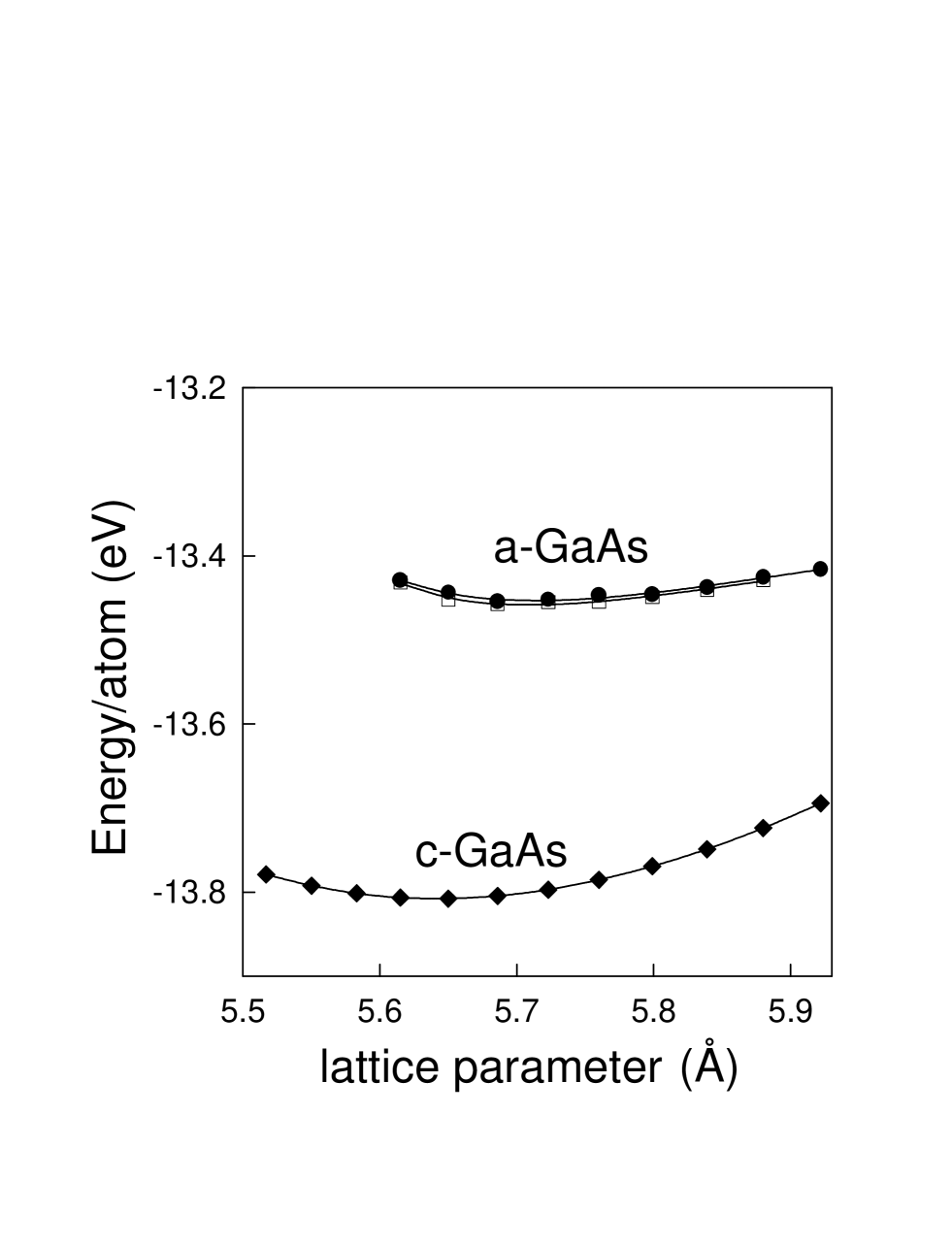
Studies of a-GaAs obtained by quenching from the liquid phase have been carried out by Molteni, Colombo and Miglio (MCM) [37], and Seong and Lewis (SL) [107]. This material has a relatively small ionicity; the TB-potential proposed by Molteni et al. [106], already discussed in Section III D, deals with charge-transfer effects by introducing a screened electrostatic term, thus keeping the potential short range. In both cases, 64-atom cells were used and the cooling rates were similar ( K/s for MCM, 50% slower for SL). One important difference however is in the choice of density: while MCM fixed it at the crystalline value, SL chose to optimise it; a density 3.2% smaller than the crystalline one was thus obtained (Fig. 15), in agreement with experiment — values in the range 4.98–5.11 g/cm3 have been reported; the crystalline value is 5.32 g/cm3. Optimisation of the density also leads to significant, and perhaps unexpected, differences between the two structures: MCM find the bonding environments of As and Ga to be symmetric, that is the two species exhibit similar distributions of coordination defects; in contrast, SL observe sizable differences between the two species, with Ga much more likely to be in a five-fold coordination state than As, which prefers to be in a three-fold state. Overall, however, the average coordination is almost precisely four — in fact slightly less, 3.94, certainly related to the fact that a-GaAs is less dense than c-GaAs.
TBMD has also been used to generate models for the chalcogenide glasses. Cobb and co-workers [108, 109], for instance, have quenched 62- and 216-atom models of GeSe2 from the liquid phase using the Sankey-Drabold-TB scheme [78]. The total simulation time for the 216-atom cell is 5 ps. In spite of this very short time, which leaves a large number of defects in the network, the system exhibits a well-defined optical gap of 1.72 eV, free of defect states; the static structure factor and vibrational density of states is also in reasonable agreement with experiment (Fig. 16). Most (85%) Ge atoms are fourfold coordinated with about 26% Ge having another Ge atom as one of its neighbours; a similar fraction of Se form homopolar bonds. Because of different coordination, this leads to a total density of “wrong” bonds of 10.8%. Cobb et al., furthermore, find that the localised electronic states are far from the band edges, thus leaving a wide, state-free gap.
Because GeSe2 is significantly less ionic than, e.g., SiO2, the timescale needed to obtain a chemically-ordered GeSe2 glass is well beyond the reach of TBMD. This is true also of the III-V compound a-GaAs. As a result, the melt-and-quench simulations of a-GaAs mentioned above lead to a density of defects which is large. Wrong bonds, for instance, are found to be in concentrations of 12.2 and 12.9% in the models of SL and MCM, respectively. While the exact number is not known from experiment, these values are most certainly on the high side. The full TBMD melt-and-quench cycle can be partly bypassed through a combination of approaches. As noted already, there exists not equivalent, in the case of III-V compounds, to the Wooten-Winer-Weaire model for a-Si; however, even though this model is “non-physical” (the topology is distorted in an ad hoc manner), it nevertheless yields structures in excellent agreement with experiment. In the same spirit — i.e., the end justifies the means — Mousseau and Lewis [75, 76] have proposed a scheme for a-GaAs based on empirical potentials that compares favourably with melt-quenched models, as we discuss now.
Amorphous covalently-bonded semiconductors have traditionally been described in terms of CRN’s. Polk’s CRN [64], presumably appropriate to a-Si, consists of a collage of corner-sharing tetrahedra which preserves the ideal coordination of four. The Connell-Temkin CRN [110] is similar, except for the additional constraint that odd-membered rings are not permitted. This model is likely relevant to chemically-ordered binary compounds since the presence of odd-membered rings necessarily imply the presence of wrong-bond defects. That a-GaAs is indeed akin to the Connell-Temkin model has been recently established by Mousseau and Lewis [75, 76]. This was done using a combination of approaches as follows: Starting with a 216-atom supercell in a random state, “zeroth-order” models were generated using Barkema and Mousseau’s activation-relaxation technique (ART), the relaxation being carried out using a simple Stillinger-Weber-like potential with and without an additional term between like atoms; these structures were then relaxed using the MCM-TBMD model. Mousseau and Lewis have found the Connell-Temkin-type network to have significantly lower energy than the Polk-type network and therefore to provide a better representation of a-GaAs as can be seen in Tables VII and VIII. However, the same structures with Ga and As replaced by Si and relaxed using the GSP-TBMD showed no difference in energy, indicating that both models have the same inherent strain level. This last result is rather surprising: the density of odd-membered rings is apparently not determined by elastic constraints but, simply, by entropic considerations.
Following the static minimisation stage, both GaAs models were relaxed at finite temperature (300 K for 7 ps and 700 K for 8.8 ps) to assess their stability and compute their dynamical properties. It was found that the Polk CRN for GaAs is unstable and in fact distorts significantly at temperatures as low as 700 K while the Connell-Temkin CRN remains relatively unaffected by the annealing process. However, a detailed comparison of the structural, vibrational and electronic properties of the two networks reveals little qualitative differences between them, indicating that intermediate-range order plays a relatively minor role in determining the properties of GaAs. It appears that only direct measurements of the density of wrong bonds can shed light on the experimental nature of the structure of a-GaAs.
D Surfaces of amorphous semiconductors
Surfaces clearly play an important role in the microelectronic properties of devices and in particular influence the growth process. However, there has been relatively few simulations of disordered-material surfaces (including growth) in the TB framework, possibly because these require, to start with, realistic (and large enough) sample of the bulk amorphous phase. It is important to note that the timescale for growth by atom deposition is much shorter in computer models than in real experiments, so that it is difficult to extract quantitative information from such simulations.
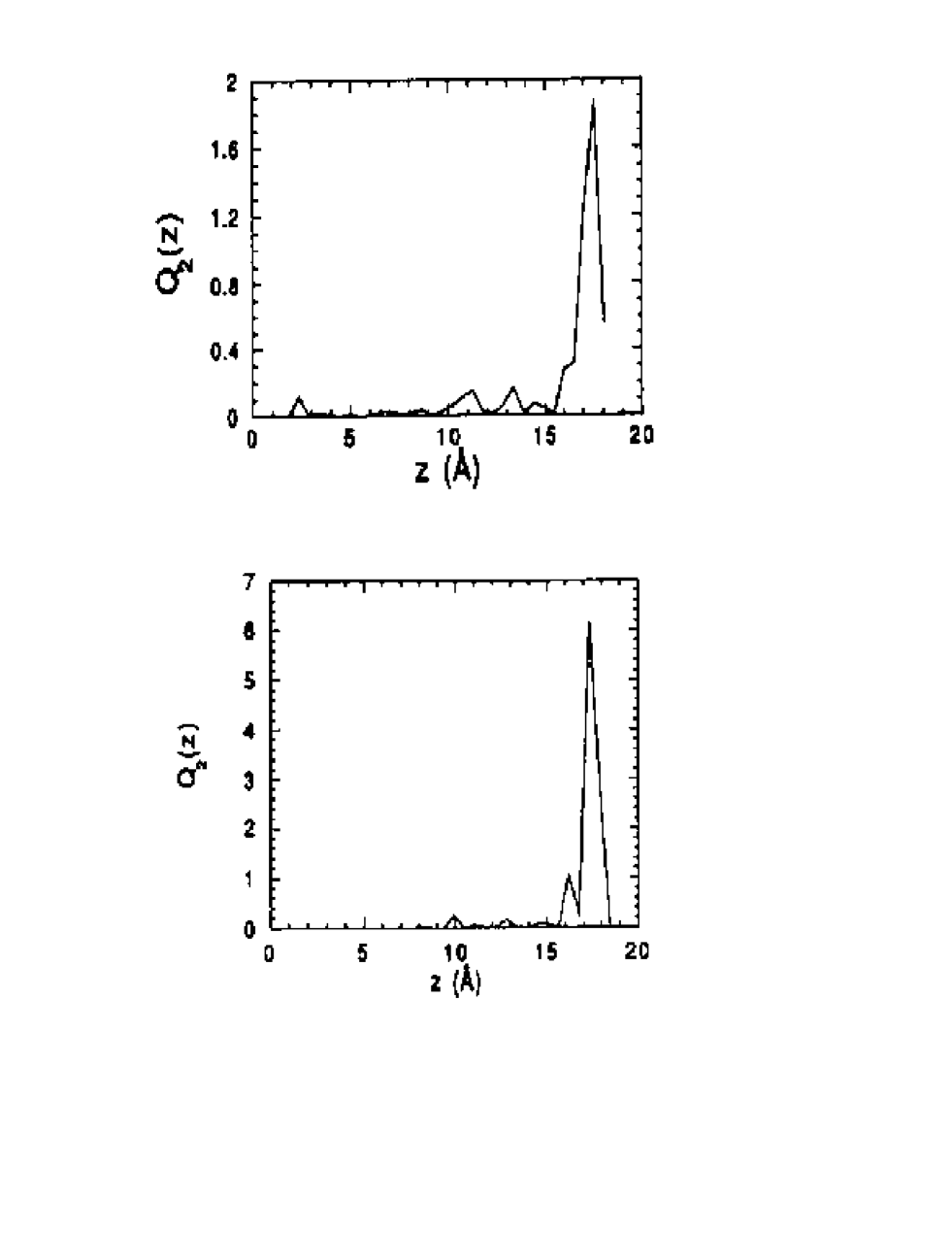
Kilian et al.[113] have used the ab initio TB scheme of Sankey and Drabold[78] to study the surface states of a-Si and a-Si:H. A 216-atom Wooten-Weiner-Weaire model of a-Si [65, 66] was first relaxed using TBMD. The periodic boundary condition was then removed along the direction and the bottom layer passivated with hydrogen; the top layer, finally, was relaxed with and without hydrogen in order to study localised electronic surface states and the effect of hydrogenation on them. In order to do this, a local charge for atom is defined, where E is the energy eigenstate. One may then calculate the mean square charge of a “layer” located at position and containing atoms:
Multiplying this quantity by gives a measure of the localisation of charge in the layer, ; in this way, the decay of surface states with depth can be monitored. Figs. 17 and 18 show some surface defects — not necessarily topological – and the corresponding spatial localisation of charge. Hydrogenating the surface does not eliminate these states, however, contrary to what often happens in the bulk: Fig. 18 shows that surface states are more localised by the addition of hydrogen but not otherwise affected. The study of other a-Si:H models [114] lead to similar conclusions: surface states seem to be difficult to eliminate. It should be noted however that, again because of computational limitations, the surfaces may not be fully relaxed. It remains to be seen if detailed thermal annealing would decrease the influence of localised surface states.
V Concluding remarks
Tight-binding molecular dynamics has contributed significantly to our understanding of defects in semiconductors. Because it is generally reliable, and yet economical from the computational viewpoint, the method constitutes an excellent complement to ab initio calculations. While the latter is limited to small unit cells, for which self-interaction of defects remains important, it is possible with TBMD to deal with systems containing many hundreds of atoms in a fully-relaxed configuration. With the advent of methods, it becomes feasible to carry out TBMD studies of more complex defects involving many tens of atoms, a task which is at present beyond the reach of ab initio approaches.
The study of amorphous semiconductors has also greatly benefited from TBMD calculations. With the wide range of local environments found in these materials, it is difficult to construct a fully satisfactory empirical potential; TB models have proved much more transferable. However, because of the computational cost of TB calculations, still much larger than classical potentials, and the difficulty of implementing methods for these materials, simulations have been limited to, principally, 64-atom cells with some noteworthy exceptions up to 512-atom cells. Using a mixture of hands-on or empirical approaches and TBMD for creating the initial structures can compensate for the increased computational cost. In spite of the biases that they possibly introduce, such mixed approaches appear to be the best, at present, for studying large, low-strain disordered structures.
The examples presented in this article underline the important contributions of TBMD calculations to the study of semiconductors. As the method becomes more widespread and fundamentals are established, it can be expected that several of the questions left unanswered in this review will be addressed in the coming years.
VI Acknowledgements
We are grateful the many people who have aroused our interest in this field and who have helped us in one way or another, in particular L. Colombo, E. Hernandez, I. Kwon, and H. Seong. This work was supported by grants from the Natural Sciences and Engineering Research Council (NSERC) of Canada and the “Fonds pour la formation de chercheurs et l’aide à la recherche” of the Province of Québec.
REFERENCES
- [1] E-mail: lewis@physcn.umontreal.ca
- [2] E-mail: mousseau@helios.phy.ohiou.edu
- [3] See for instance M.P. Allen and D.J. Tildesley, Computer Simulation of Liquids (Clarendon, Oxford 1987).
- [4] See for instance M.C. Payne, M.P. Teter, D.C. Allan, T.A. Arias, and J.D. Joannopoulos, Rev. Mod. Phys. 64, 1045 (1992).
- [5] G. Galli, Curr. Opin. in Sol. Sta. and Mater. Sci. 1, 864 (1996).
- [6] For a review of TB and other electronic structure methods, see, for example, W.A. Harrison, Electronic Structure and the Properties of Solids (Dover, New York, 1989).
- [7] C. M. Goringe, D. R. Bowler, and E. Hernandez, Rep. Prog. Phys. 60, 1447 (1997).
- [8] D. Porezag, Th. Frauenheim, Th. Köhler, G. Seifert, and R. Kaschner, Phys. Rev. B 51, 12947 (1995).
- [9] J. Harris, Phys. Rev. B 31, 1770 (1985).
- [10] M. Lannoo and J. Bourgoin, Point defects in semiconductors I (Springer, Berlin, 1981) vol. 22; J. Bourgoin and M. Lannoo, Point defects in semiconductors II (Springer, Berlin, 1983), vol. 35.
- [11] C.Z. Wang, C.T. Chan, and K.M. Ho, Phys. Rev. Lett. 66, 189 (1991).
- [12] L. Goodwin, A.J. Skinner, and D.G. Pettifor, Europhys. Lett. 9, 701 (1989).
- [13] J. L. Mercer and M. Y. Chou, Phys. Rev. B 43, 6768 (1991).
- [14] I. Kwon, R. Biswas, C.Z. Wang, K.M. Ho, and C.M. Soukoulis, Phys. Rev. B 49, 7242 (1994).
- [15] T.J. Lenosky, J.D. Kress, I. Kwon, A.F. Voter, B. Edwards, D.F. Richards, S. Yang, and J.B. Adams, Phys. Rev. B 55, 1528 (1997).
- [16] G.A. Baraff and M. Schlüter, Phys. Rev. B 30, 3460 (1984).
- [17] P.J. Kelly and R. Car, Phys. Rev. B 45, 6543 (1992).
- [18] H. Seong and L.J. Lewis, Phys. Rev. B 53, 9791 (1996).
- [19] E.G. Song, E. Kim, Y.H. Lee, and Y.G. Hwang, Phys. Rev. B 48, 1486 (1993).
- [20] G.D. Watkins, in Deep Centers in Semiconductors: A State-of-the-Art Approach, edited by S.T. Pantelides (Gordon and Breach, New York, 1986), p. 147.
- [21] G.A. Baraff, E.O. Kane, and M. Schlüter, Phys. Rev. B 21, 3562 (1980); 21, 5662 (1980).
- [22] M. Tang, L. Colombo, J. Zhu, and T. Diaz de la Rubia, Phys. Rev. B 55, 14279 (1997).
- [23] St. Bausch, H. Zillgen, and P. Ehrhart, unpublished.
- [24] N. Bernstein and E. Kaxiras, Phys. Rev. B 56, 10488 (1997).
- [25] P.B. Rasband, A.P. Horsfield, and P. Clancy, Philos. Mag. B 73, 71 (1996).
- [26] P.W. Anderson, Phys. Rev. Lett. 34, 953 (1975).
- [27] P.B. Rasband, P. Clancy, and M.O. Thompson, J. Appl. Phys. 79, 8998 (1996).
- [28] N.O. Lipari, J. Bernholc, and S.T. Pantelides, Phys. Rev. Lett. 43, 1354 (1979).
- [29] A. Bongiorno, L. Colombo, and T. Diaz de la Rubia, submitted.
- [30] S. Goedecker and L. Colombo, Phys. Rev. Lett. 73, 122 (1994).
- [31] W.G. Li and C.W. Myles, Phys. Rev. B 43, 9947 (1991).
- [32] H.P. Hjalmarson, P. Vogl, D.J. Wolford, and J.D. Dow, Phys. Rev. Lett. 44, 810 (1980).
- [33] W.A. Harrison, Phys. Rev. B 27, 3592 (1983); see also Ref. [6].
- [34] P. Vogl, H.P. Hjalmarson, and J.D. Dow, J. Phys. Chem. Solids 44, 365 (1983).
- [35] C.S. Nichols, C.G. Van de Walle, and S.T. Pantelides, Phys. Rev. B 40, 5484 (1989).
- [36] H. Seong and L.J. Lewis, Phys. Rev. B 52, 5675 (1995).
- [37] C. Molteni, L. Colombo, and L. Miglio, Europhys. Lett. 24, 659 (1993): Phys. Rev. B 50, 4371 (1994).
- [38] K. Laasonen, R.M. Nieminen, and M.J. Puska, Phys. Rev. B 45, 4122 (1992); L. Gilgien, G. Galli, F. Gygi, and R. Car, Phys. Rev. Lett. 72, 3214 (1994).
- [39] K. Saarinen, P. Hautojärvi, P. Lanki, and C. Corbel, Phys. Rev. B 44, 10585 (1991).
- [40] K. Saarinen, S. Kuisma, P. Hautojärvi, C. Corbel, and C. LeBerre, Phys. Rev. Lett. 70, 2794 (1993); J.P. Peng, K.G. Lynn, M.T. Umlor, D.J. Keeble, and D.R. Harshman, Phys. Rev. B 50 11 247 (1994).
- [41] J. Dabrowski and M. Scheffler, Phys. Rev. B 40, 10391 (1989).
- [42] D.J. Chadi and K.J. Chang, Phys. Rev. Lett. 60, 2187 (1988).
- [43] G.B. Bachelet and M. Scheffler, in Proceedings of the 17th International conference on the Physics of semiconductors, edited by D.J. Chadi and W.A. Harrison (Springer, Berlin, 1985), p. 755.
- [44] R.M. Feenstra, J.M. Woodall, and G.D. Pettit, Phys. Rev. Lett. 71, 1176 (1993).
- [45] S.B. Zhang and D.J. Chadi, Phys. Rev. Lett. 64, 1789 (1990).
- [46] D.J. Chadi and K.J. Chang, Phys. Rev. Lett. 60, 2187 (1988).
- [47] G.A. Baraff and M. Schlüter, Phys. Rev. Lett. 55, 2340 (1985).
- [48] H.J. von Bardeleben, D. Stievenard, D. Deresmes, A. Huber, and J.C. Bourgoin, Phys. Rev. B 34, 7192 (1986).
- [49] K. Saarinen, S. Kuisma, P. Hautojärvi, C. Corbel, and C. LeBerre, Phys. Rev. B 49, 8005 (1994).
- [50] C. Ziegler, U. Scherz, and M. Scheffler, Phys. Rev. B 47, 16624 (1993).
- [51] F.H. Stillinger and T.A. Weber, Phys. Rev. B 31, 5262 (1985).
- [52] U. Gosële, A. Plössl, and T.Y. Tan, in Process Physics and Modeling in Semiconductor Technology, edited by G.R. Srinivasan, C.S. Murthy, and S.T. Dunham (Electrochemical Society, Pennington, NJ, 1996), p. 309.
- [53] G. Boisvert, L.J. Lewis and A. Yelon, Phys. Rev. Lett. 53, 469, 1995.
- [54] F. Cargnoni, L. Colombo and C. Gatti, Nucl. Instr. Meth. in Phys. Res. B 127/128, 235 (1997).
- [55] F. Cargnoni, C. Gatti, and L. Colombo, Phys. Rev. B xx, xxxx (199x).
- [56] G. Panzarini and L. Colombo, Phys. Rev. Lett. 73, 1636 (1994); see also L. Colombo, in Annual Reviews of Computational Physics, vol.IV (edited by D. Stauffer, World Scientific, Singapore, 1996), p.147.
- [57] F. Buda, G.L. Chiarotti, R. Car, and M. Parrinello, Phys. Rev. Lett. 63, 294 (1989).
- [58] D.E. Boucher and G.G. DeLeo, Phys. Rev. B 50, 5247 (1994).
- [59] V.A. Gordeev et al., unpublished.
- [60] R.F. Kiefl et al., Phys. Rev. Lett 126, 516 (1986).
- [61] J. Tersoff, Phys. rev. B 38, 9902 (1988).
- [62] R. Biswas and D. R. Hamann, Phys. Rev. B 36, 6434 (1987).
- [63] M. Z. Bazant, E. Kaxiras and J. F. Justo, Phys. Rev. B 56, 8542 (1997).
- [64] D.E. Polk, J. Non-Cryst. Sol. 5, 365 (1971).
- [65] F. Wooten, K. Winer, and D. Weaire, Phys. Rev. Lett. 54, 1392 (1985).
- [66] F. Wooten and D. Weaire, Solid State Physics 40, 1 (1987).
- [67] G.T. Barkema and N. Mousseau, Phys. Rev. Lett. 77, 4358 (1996).
- [68] N. Mousseau and G. T. Barkema, Phys. Rev. E 57, 2419 (1998).
- [69] E. Kim and Y.H. Lee, Phys. Rev. B 49, 1743 (1994).
- [70] R. Virkunnen, K. Laasonen and R. M. Nieminen, J. Phys.: Cond. Mat. 3, 7455 (1991).
- [71] I. Stich, R. Car, and M. Parrinello, Phys. Rev. B 44, 11092 (1991).
- [72] C. Z. Wang, C. T. Chan and K. M. Ho, Phys. Rev. B 45, 12227 (1992).
- [73] S. Roorda, W. C. Sinke, J. M. Poate, D. C. Jacobson, S. Dierker, B. S. Dennis, D. J. Eaglesham, F. Spaepen and P. Fuoss, Phys. Rev. B 44, 3702 (1991).
- [74] G. Servalli and L. Colombo, Europhys. Lett. 22, 107 (1993).
- [75] N. Mousseau and L.J. Lewis, Phys. Rev. Lett. 78, 1484 (1997).
- [76] N. Mousseau and L. J. Lewis, Phys. Rev. B 56, 9461 (1997).
- [77] D. A. Drabold, P. A. Fedders, O. F. Sankey and J. D. Dow, Phys. Rev. B 42, 5135 (1990).
- [78] O. F. Sankey and D. J. Niklewski, Phys. Rev. B 40, 3979 (1989); O. F. Sankey, D. J. Niklewski, D. A. Drabold, and J. D. Dow, Phys. Rev B 41, 12750 (1990); O. F. Sankey and D. A. Drabold, Bull. Am. Phys. Soc. 36, 924 (1991).
- [79] D. A. Drabold, P. A. Fedders, S. Klemm and O. F. Sankey, Phys. Rev. Lett. 67, 2179 (1991).
- [80] P. A. Fedders, D. A. Drabold and S. Klemm, Phys. Rev. B 45, 4048 (1992).
- [81] G. De Sandre, L. Colombo and C. Bottani, Phys. Rev. B 54, 11857 (1996).
- [82] J. M. Holender and G. J. Morgan, J. Cond. Mat. 4, 4473 (1992).
- [83] J. Dong and D. A. Drabold, Phys. Rev. Lett. 80, 1928 (1998).
- [84] B.R. Djordjević, M.F. Thorpe, and F. Wooten, Phys. Rev. B 52, 5685 (1995).
- [85] C. Z. Wang, K. M. Ho and C. T. Chan, Phys. Rev. Lett. 70, 611 (1993).
- [86] F. Li and J. S. Lannin, Phys. Rev. Lett. 65, 1905 (1990).
- [87] C. Z. Wang and K. M. Ho, Phys. Rev. Lett. 71, 1184 (1993).
- [88] D. A. Drabold, P. A. Fedders, P. Stumm, Phys. Rev. B 49, 16415 (1994).
- [89] I.-H. Lee and K. J. Chang, Phys. Rev. B 50, 18083 (1994).
- [90] Th. Köhler, Th. Frauenheim and G. Jungnickel, Phys. Rev. B 52, 11837 (1995).
- [91] J. M. Holender, G. J. Morgan and R. Jones, Phys. Rev. B 47, 3991 (1993).
- [92] Q. Li and R. Biswas, Phys. Rev. B 50, 18090 (1994).
- [93] P. A. Fedders and D. A. Drabold, Phys. Rev. B 47, 13227 (1993).
- [94] Y. K. Park and C. W. Myles, Phys. Rev. B 51, 1671 (1995).
- [95] B. Tuttle and J. B. Adams, Phys. Rev. B 53, 16265 (1996).
- [96] S. Lanzavecchia and L. Colombo, Europhys. Lett. 36, 295 (1996).
- [97] A. Menelle, Ph. D. Thesis, Université Pierre et Marie Curie (Paris IV), 1987.
- [98] D.L. Staebler and C. R. Wronski, Appl. Phys. Lett. 31, 292 (1997).
- [99] P. A. Fedders, Phys. Rev. B 52, 1729 (1995).
- [100] R. Biswas, Q. Li, Y. Yoon and H. M. Branz, Phys. Rev B 56, 9197 (1997).
- [101] L. Guttman and C. F. Fong, Phys. Rev. B 26, 6756 (1982).
- [102] P. A. Fedders and D. A. Drabold, Phys. Rev. B 53, 3841 (1996).
- [103] B. Tuttle and J. B. Adams, Phys. Rev. B 56, 4565 (1997).
- [104] R. Biswas, Q. Li, B. C. Pan and Y. Yoon, Phys. Rev. B 57, 2253 (1998).
- [105] P. Stumm and D. A. Drabold, Phys. Rev. Lett. 79, 677 (1997).
- [106] C. Molteni, L. Colombo, and L. Miglio, J. Phys.: Condens. Matter 6, 5243 (1994).
- [107] H. Seong and L.J. Lewis, Phys. Rev. B 53, 4408 (1996).
- [108] R. L. Cappelletti, M. Cobb, D. A. Drabold and W. A. Kamitakahara, Phys. Rev. B 52, 9133 (1995).
- [109] M. Cobb, D. A. Drabold, and R. L. Cappelletti, Phys. Rev. B 54, 12162 (1996).
- [110] G.A.N. Connell and R.J. Temkin, Phys. Rev. B 9, 5323 (1974).
- [111] E. Fois, A. Selloni, G. Pastore, Q.-M. Zhang, and R. Car, Phys. Rev. B 45, 13 378 (1992).
- [112] F. Buda, G. L. Chiarotti, R. Car, and M. Parrinello, Phys. Rev. B 44, 5908 (1991).
- [113] K. A. Kilian, D. A. Drabold, and J. B. Adams, Phys. Rev. B 48, 17393 (1993).
- [114] K. A. Kilian, Mod. Sim. Mater. Scien. Eng. 5, 549 (1997).
| GSP | GSP | GSP | MC | KBHS | KBHS | LKKVERYA | LKKVERYA | LDA | |
| References | [11, 19] | [11] | [11] | [13] | [14] | [14] | [15] | [15] | [16, 17, 18] |
| Defect | |||||||||
| Monoacancy | 3.67 (1.35) | 3.96 (1.86) | 4.12 (1.91) | 3.76 | 3.46 (1.26) | 3.93 (1.64) | 3.40 (0.24) | 3.78 (0.20) | 3.3–4.3 (0.4–0.6) |
| T interstitial | 4.39 (2.13) | 4.40 (2.14) | 4.41 (2.14) | 4.95 | 3.61 (0.51) | 4.42 (0.49) | 3.55 (0.59) | 3.7–4.8 (0.1–0.2) | |
| H interstitial | 5.78 (4.30) | 5.90 (4.42) | 5.93 (4.42) | 4.75 (1.17) | 5.13 (1.23) | 3.56 (0.89) | 4.3–5.0 (0.6–1.1) | ||
| Divacancy | 5.68 (1.73) | 4.32 (0.27) | |||||||
| Split divacancy | 6.54 (2.43) | 5.90 (0.57) | |||||||
| Frenkel pair | 6.55 (3.89) |
| Defect | GSP-TBMD | LDA |
|---|---|---|
| Monoacancy | 0.76 | 0.23 |
| T interstitial | 0.52, 0.12 | |
| Divacancy | 1.00, 0.46 | 0.04 |
| Split divacancy | 0.76, 0.46, 0.34 | 0.08 |
| Frenkel pair | 0.76, 0.52 |
| System | Bond length | TB | TBMD | Experiment |
|---|---|---|---|---|
| Å | eV | eV | eV | |
| GaP:N | 2.15 | 2.10 | 2.25 | 2.34 |
| GaP:O | 2.78 | 1.85 | 1.70 | 1.46 |
| GaP:PGa | 2.28 | 1.03 | 1.09 | 1.10 |
| GaP:Ge | 2.24 | 1.85 | 1.95 | 2.16 |
| GaP:Se | 2.22 | 2.32 | C.B. | |
| Si:S | 2.23 | 0.58 | 0.63 | 0.85 |
| Si:Se | 2.03 | 0.65 | 0.83 | 0.86 |
| Si:Te | 2.60 | 1.12 | 1.05 | 1.01 |
| Si:C | 1.98 | 1.09 | C.B. |
| Defect | Breathing (Å) | Average (Å) | Average (%) | ||||
|---|---|---|---|---|---|---|---|
| 1 | 2 | 3 | 4 | ||||
| -0.31 | -0.35 | -0.31 | -0.31 | -0.32 | -13.1 | -34.3 | |
| -0.33 | -0.33 | -0.31 | -0.30 | -0.32 | -13.0 | -34.1 | |
| -0.32 | -0.32 | -0.32 | -0.29 | -0.32 | -12.9 | -33.9 | |
| -0.32 | -0.32 | -0.32 | -0.30 | -0.31 | -12.8 | -33.7 | |
| -0.31 | -0.31 | -0.31 | -0.31 | -0.31 | -12.8 | -33.7 | |
| 0.38 | 0.38 | 0.38 | 0.38 | 0.38 | 15.5 | 54.0 | |
| 0.44 | 0.44 | 0.44 | -0.49 | 0.21 | 8.5 | 24.2 | |
| 0.39 | 0.39 | 0.39 | -0.50 | 0.17 | 6.8 | 18.9 | |
| 0.45 | -0.42 | 0.45 | -0.42 | 0.02 | 0.8 | -3.3 | |
| Ga | 0.49 | 0.49 | 0.21 | 0.21 | 0.35 | 14.4 | 50.0 |
| Ga | 0.48 | 0.17 | 0.13 | 0.13 | 0.23 | 9.2 | 30.0 |
| Ga | 0.48 | 0.07 | 0.07 | 0.07 | 0.17 | 7.0 | 22.2 |
| Ga | 0.11 | 0.02 | 0.02 | 0.02 | 0.04 | 1.8 | 5.5 |
| Ga | -0.01 | -0.01 | -0.01 | -0.01 | -0.01 | -0.3 | -1.0 |
| As | 0.06 | 0.06 | 0.06 | 0.06 | 0.06 | 2.5 | 7.6 |
| As | 0.06 | 0.06 | 0.06 | 0.06 | 0.06 | 2.4 | 7.5 |
| As | 0.06 | 0.06 | 0.06 | 0.06 | 0.06 | 2.4 | 7.5 |
| As | 0.06 | 0.06 | 0.06 | 0.06 | 0.06 | 2.5 | 7.8 |
| Defect | Pairing 1 (Å) | Pairing 2 (Å) | ||||||
|---|---|---|---|---|---|---|---|---|
| 1 | 2 | 3 | 4 | 1 | 2 | 3 | 4 | |
| 0 | 0 | 0 | 0 | 0 | 0 | 0 | 0 | |
| -0.01 | -0.01 | 0.03 | 0 | 0.02 | 0.02 | 0 | 0 | |
| -0.01 | -0.01 | 0.02 | 0 | 0 | 0 | 0 | 0 | |
| 0.01 | -0.01 | 0.01 | -0.01 | -0.01 | 0.01 | -0.01 | 0.01 | |
| Ga | -0.02 | -0.02 | -0.21 | -0.21 | 0 | 0 | 0 | 0 |
| Ga | 0.03 | -0.01 | -0.12 | -0.12 | 0 | 0 | -0.03 | 0.03 |
| Ga | 0 | 0.08 | -0.04 | -0.04 | 0 | 0 | -0.06 | 0.06 |
| Ga | 0 | 0.05 | -0.03 | -0.03 | 0 | 0 | -0.05 | 0.05 |
| Ga | 0 | 0 | 0 | 0 | 0 | 0 | 0 | 0 |
| CP | ML | KL | DFSD | SCA | SCB | |
| 0.002 | 0.032 | 0.032 | 0.063 | 0.049 | 0.009 | |
| 0.966 | 0.954 | 0.828 | 0.877 | 0.904 | 0.958 | |
| 0.032 | 0.014 | 0.125 | 0.060 | 0.047 | 0.033 | |
| 0 | 0 | 0.016 | 0 | |||
| Z | 4.03 | 3.98 | 4.28 | 4.00 | 3.99 | 4.02 |
| 3.0 | 3.0 | 2.75 | 2.70 | 2.82 | 2.82 | |
| 106.7 | 109.4 | 108.3 | ||||
| 16.3 | 9.4 | 15.5 | ||||
| # atoms | 64 | 216 | 64 | 63 | 64 | 64 |
| CRN-P | CRN-CT | SL | MCM | CP | |||
| 0 K | 300 K | 0 K | 300 K | 0 K | 0 K | 0 K | |
| 3 | 0.046 | 0.128 | 0.051 | 0.118 | 0.242 | 0.14 | 0.219 |
| 4 | 0.954 | 0.845 | 0.944 | 0.830 | 0.598 | 0.66 | 0.781 |
| 5 | 0 | 0.026 | 0.005 | 0.045 | 0.129 | 0.18 | 0 |
| 6 | 0 | 0.001 | 0 | 0.004 | 0.024 | 0 | |
| 7 | 0 | 0.000 | 0 | 0.002 | 0.007 | 0 | |
| 3.95 | 3.90 | 3.95 | 3.95 | 3.94 | 4.09 | 3.83 | |
| (Å) | 3.0 | 3.1 | 3.0 | 3.1 | 3.0 | 3.0 | 2.8 |
| (Å) | 2.508 | 2.505 | 2.517 | 2.507 | |||
| (Å) | 0.075 | 0.117 | 0.073 | 0.103 | |||
| Wrong bonds (%) | 14.1 | 14.2 | 3.9 | 5.2 | 12.2 | 12.9 | 10.0 |
| (deg.) | 11.0 | 14.1 | 10.8 | 15.0 | 17.0 | 17.0 | |
| Network | Si | GaAs | GaAs (SL) |
|---|---|---|---|
| CRN-P | -13.172 | -13.450 | |
| CRN-CT | -13.163 | -13.561 | -13.450 |
| Crystal | -13.389 | -13.802 | -13.802 |
![[Uncaptioned image]](/html/cond-mat/9803330/assets/x1.png)
![[Uncaptioned image]](/html/cond-mat/9803330/assets/x2.png)
![[Uncaptioned image]](/html/cond-mat/9803330/assets/x3.png)
![[Uncaptioned image]](/html/cond-mat/9803330/assets/x4.png)
![[Uncaptioned image]](/html/cond-mat/9803330/assets/x5.png)
![[Uncaptioned image]](/html/cond-mat/9803330/assets/x6.png)
![[Uncaptioned image]](/html/cond-mat/9803330/assets/x7.png)
![[Uncaptioned image]](/html/cond-mat/9803330/assets/x8.png)
![[Uncaptioned image]](/html/cond-mat/9803330/assets/x9.png)