Electrical properties of a-antimony selenide
Abstract
This paper reports conduction mechanism in a-Sb2Se3over a wide range of temperature (238K to 338K) and frequency (5Hz to 100kHz). The d.c. conductivity measured as a function of temperature shows semiconducting behaviour with activation energy E= 0.42 eV. Thermally induced changes in the electrical and dielectric properties of a-Sb2Se3have been examined. The a.c. conductivity in the material has been explained using modified CBH model. The band conduction and single polaron hopping is dominant above room temperature. However, in the lower temperature range the bipolaron hopping dominates.
Keywords. Chalcogenides glasses; amorphous
semiconductors; a.c. conductivity; electrical properties.
PAC Nos 72-20; 71-55
I Introduction
During the last few years amorphous semiconductors have been used in the manufacture of solar cells, batteries and phototransistors as well as in some steps of technological processing of very large scale integration (VLSI) microelectronics circuits [1]. Thermally induced structural and electrical effects are known to be important in inducing the memory phenomenon in semiconducting chalcogenide glasses [2]-[6]. Alzewel et al., [7, 8] have studied the electrical conductivity of powdered antimony chalcogenides. Antimony alloys have recieved great attention in the past due to semiconductivity of Sb concentration. It was reported by Mott and Devis [9] that the effect of Sb in Se is even greater than in Te in promoting crystallisation. Recently, study has been made on thin and thick films of the system ( 35, 40 and 45) [10]. Crystalline Sb2Se3has been prepared and studied by several workers [11, 12]. Antimony triselenide (band gap 1.2 eV), [13] a p-type semiconductor having an orthorhombic structure with unit cell dimensions [14] is used in preparation of recording optical laser disc and as an insulating material in MIS solar cells. The preparation and study of amorphous-Sb2Se3can throw light on the possible applications of this material in that form. Measurements of electrical properties of a-Sb2Se3are reported in this paper over a wide temperature and frequency range. Results indicate that electrical properties can be explained on the basis of widely accepted modified-Correlated Barrier Hopping (m-CBH) model for chalcogenide glasses.
II Experimental Details
Ingots of glassy material Sb2Se3were prepared by melt quench method. The 99.99% pure elements were sealed in an evacuated ( torr) quartz ampoule (12mm diameter and 160mm long). The ampoule was heated in a muffle furnace at the reaction temperature (630 C for 24 hr). The composition (Sb:Se:1:1) of the glasses was determined by EDAX and amorphous nature was verified by X-ray diffraction pattern obtained using by X-ray diffractometer (Philips PW 1130/60). The pellets of 0.677 cm diameter were prepared in the hydraulic press at a pressure of .
The measurements were carried out in a specially designed vacuum cell in the temperature range 233 to 313 K and frequencies from 6 Hz to 100 kHz. A sophisticated computer controlled ac-impedance system (Model 5206, EG & G, PARC USA) was used for the measurements [17]. Polished samples with a thickness 0.04-0.10 cm and area 0.36 cm2 were put in contact with aquadag (a conducting emulsion) in a sandwich configuration. The sample was kept in vacuum in a copper sample holder ensuring no temperature gradient between the electrods and the sample. The effect of temperature is studied by using a closed cycle refrigerator (Model F-70, Julabo) was used to obtain different temperatures, which can maintain constant temperature within 1 K for all the measurements. Ohmic contacts were confirmed through linear I-V characterstics in the voltage range. All electrical measurements of real and imaginary components of impedance parameters ( and ) and real and imaginary component of admittance parameters ( and ) were made over a wide range of temperature (233 to 313 K ) and frequency (6 Hz to 100 kHz).
III Results and Discussion
A Dipolar behaviour of Sb2Se3
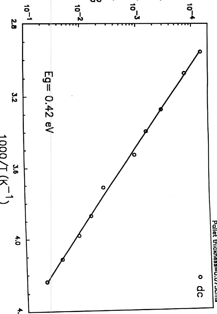
Figure 1 shows the plot of versus 1000/T which was obtained using the expression
| (1) |
The plots in Fig. 1 are found to be linear over the temperature range studied. In the above expression and is the temperature coefficient of the band gap. From the figure, the activation energy E and for the sample are found to be 0.43 eV and respectively. It has also been observed that E is constant for different pellets ( thickness = 0.04cm to 0.08 cm) with a statistical error of 0.3%.
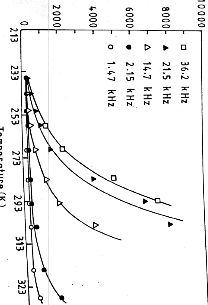
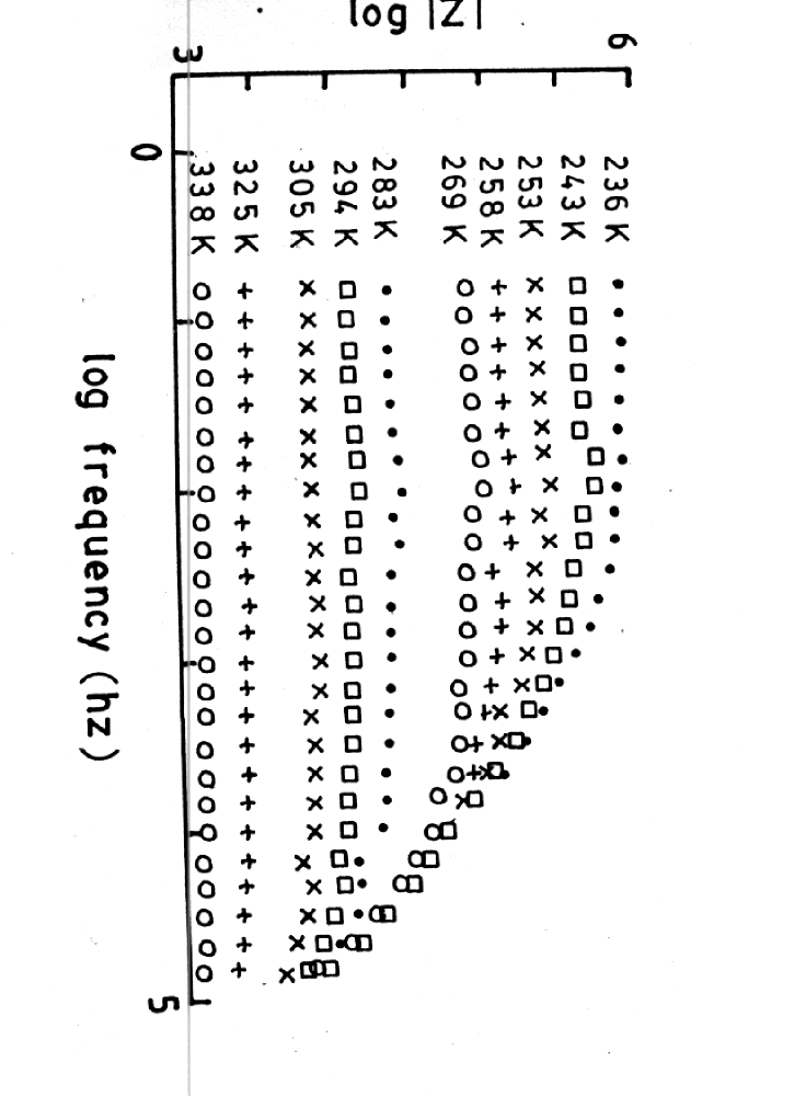
The variation of versus (Fig. 2) indicates that the impedance is sensitive to frequency at lower temperatures and gradually becomes independent of frequency with increase in temperature. This type of behaviour indicates dominance of band conduction at higher temperatures.
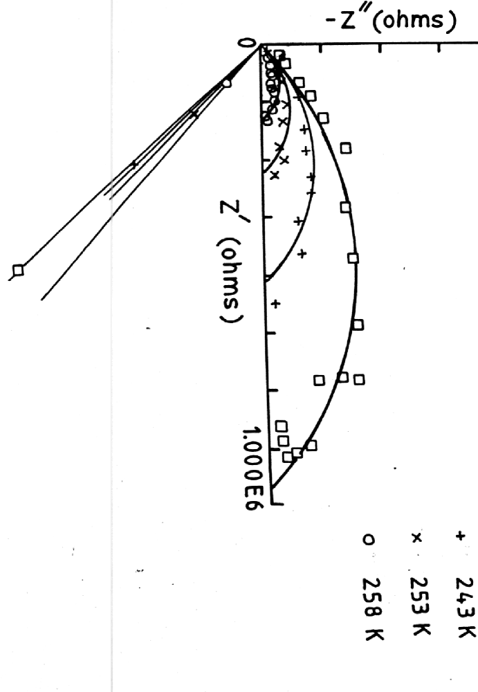
The sensitivity of Sb2Se3to temperature is shown in Fig. 3. The figure gives the Nyquist plots ( versus ) for Sb2Se3at different temperatures over the frequency range studied. The semicircular Nyquist plots indicate dipolar nature of the sample, which may be due to hopping back and forth of bipolarons between charged defects states ( D+ and D- ) reported to be present in chalcogenides [14]. The size of the Nyquist plots reduces with rise in temperature and regain their original size when temperature is increased.
The Nyquist plots for Sb2Se3form a perfect arc of a semicircle with its centre lying considerably below the abscissa (i.e., distribution parameter ). Figure 3 also gives the value of calculated at different temperatures. In dielectric materials, the finite value of the distribution parameter and a depressed arc are typical for a dipolar system involving multirelaxation processes [14]-[17]. But the dependence of on temperature indicates that the mean position of the dipole is varying with variation in temperature. The dipolar nature of Sb2Se3is further confirmed by investigating the variation of capacitance with temperature at different frequencies. It is clear from Fig. 4 that in the lower temperature range the value of C is nearly constant and it increases with increase in temperature. However the rate of change of capacitance (i.e., dC/dT) is higher for lower frequencies and decreases with increasing temperature. These results can be explained by the fact that thermally assisted hopping results in increasing the capacitance of the material. In other words, in the lower temperature range, the dipoles remain frozen and attain rotational freedom when the temperature is increased. Thus the relaxation effects are confirmed by the rate of increase in capacitance with frequency.
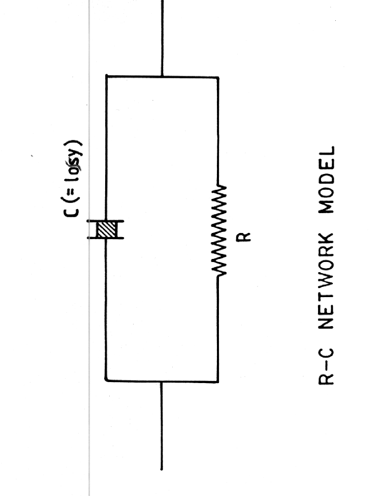
The inversion of Nyquist plots in the admittance plane are shown in the Fig. 5. It is clear from the figure that the angle of inclination is less than . This type of behaviour has been explained on the basis of R-C network model (Fig. 6), such that total impedance is given by [18]
| (2) | |||||
| (3) |
Moreover, this angle (shown in Fig. 5) is also temperature dependent. At lower temperatures (below 273 K ) it is almost constant, while after a certain temperature (276 - 278 K) it shows a sudden decrease, which implies a change in the conduction mechanism.
B CBH model for a-Sb2Se3
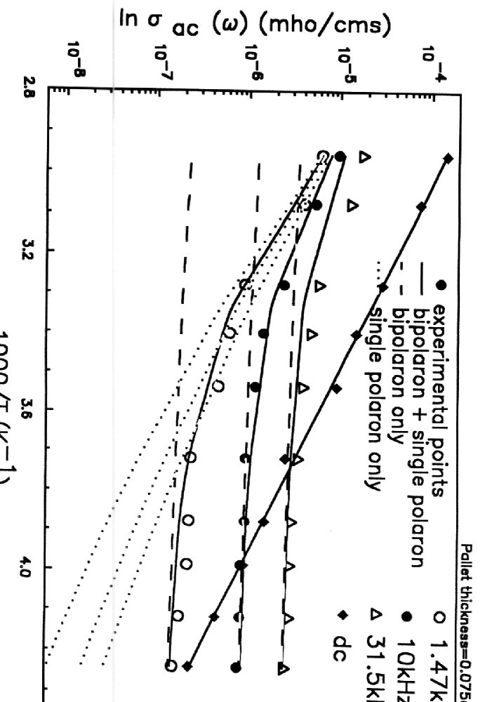
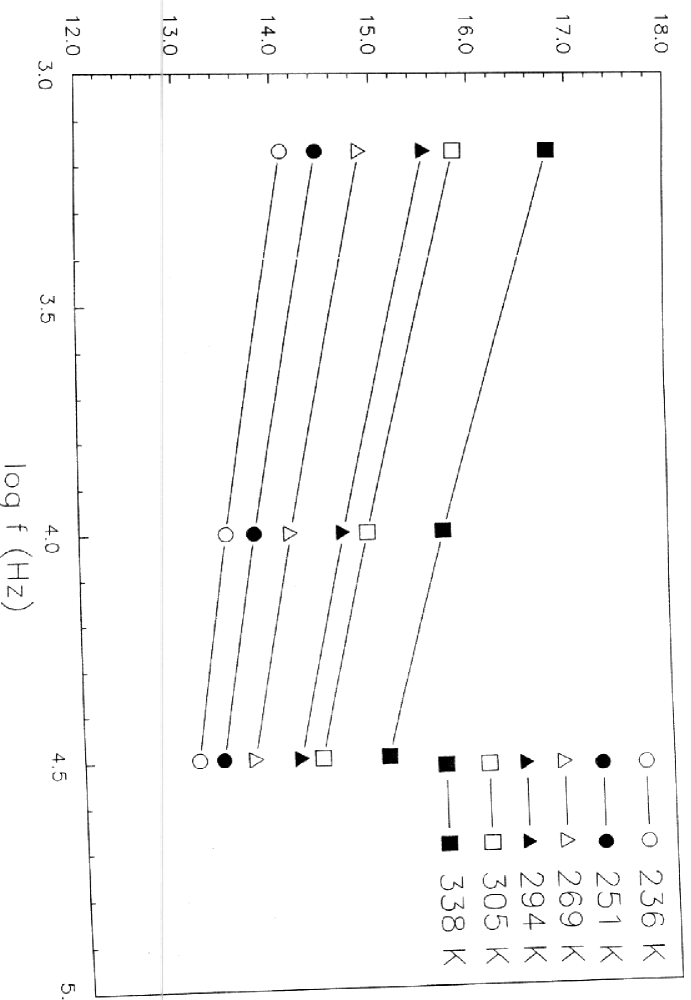
The complex impedance plots show the dipolar multi-relaxation nature of a-Sb2Se3. This behaviour is explained by the R-C network model (Fig. 6). However, this does not further elucidate the nature of conduction mechanism in this sample. Therefore a.c. conductivity at different temperatures is calculated. It is found that dispersion in the temperature dependence of curves increases at lower frequencies while it merges at higher frequencies (Fig. 7).
From the expression
| (4) |
the a.c. conductivity is obtained, where is given by Eqn.1 and its behaviour is shown in the Fig. 1. The is measured directly from lock-in-analyser (Section II). The dominates over at lower temperatures, while dominates at higher temperatures (Fig. 7).
The modified Correlated Barrier Hopping (m-CBH) model explains the experimental results reported in this paper. It states that bipolaron hopping between the charged defects states D+ and D- is responsible for the a.c. conductivity in these semiconductors. Dipolar multi-relaxation behaviour of this sample is already indicated from the Nyquist plots described in the last subsection. So the charged defect states are expected to be present in a-Sb2Se3. According to CBH model a.c. conductivity is given by [19, 20]
| (5) |
where is the number of polarons involved in the hopping process, is proportional to the square of the concentration of the states and is the dielectric constant. is the hopping distance for the conduction and is given as
| (6) |
where is the maximum barrier height and is the characteristic relaxation time for the material.
Figure 7 shows the variation of a.c. conductivity with temperature at different frequencies. It is evident from the figure that is very sensitive to temperature in the higher temperature regime. The low temperature a.c. conduction can be explained by considering bipolaron hopping between D+ and D- centers whereas the higher temperature behaviour is due to thermally activated single polaron hopping. At higher temperatures a number of thermally generated D0 centers are produced with a temperature dependent concentration [21]
| (7) |
where is the concentration of D+ or D- centers at . The defect concentration factor in Eqn. 5 is replaced by :
| (8) | |||||
| (9) |
Thus for single bipolaron hopping this factor is thermally activated and hence is also activated.
According to CBH model [22]
| (10) |
where is optical band gap, is the maximum band width and behaviour with frequency is as
| (11) |
Here [[19]],
| (12) |
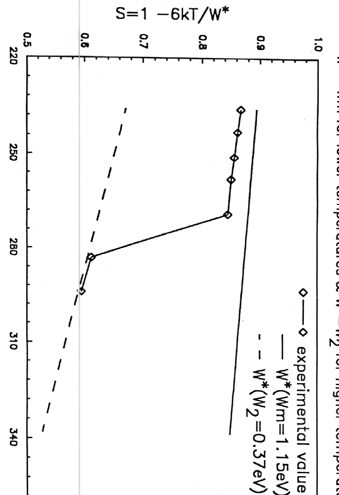
While for bipolaron hopping and for single polaron hopping. Therefore, is estimated from the values at lower temperatures. Values of , and were estimated from the values of at higher temperatures. These parameters are then fed to CBH model to fit the a.c. conductivity data calculated from the experiments. The behaviour of Eqn.12 () can be seen in the Fig. 8. This indicates that follows for lower temperatures and for higher temperatures. Figure 8 also shows a sudden change in conduction mechanism at a certain temperature (276-278K). The similar behaviour is noticed in the admittance plots (Fig. 5). The different parameters used for CBH model calculations are as following
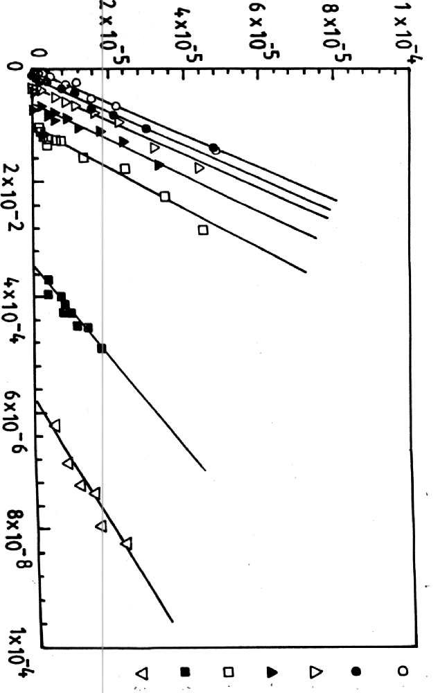
Further, the effect of temperature and frequency on the hopping length , which is a measure of the effective length of a dipole can be studied using CBH model. The variation of with frequency at different temperature is shown in the Fig. 9. The figure indicates that is more sensitive to frequency in the high temperature regime and the sensitivity decreases with decreasing temperature. Thus at low temperature, is constant with frequency, which implies a constant value of capacitance which is found to be true from the Fig. 4.
IV Conclusion
Nyquist plots or complex impedance studies confirm the dipolar nature of Sb2Se3and multi-relaxation behaviour as seen in most chalcogenide glasses. These plots also indicate that the capacitive nature dominates over the resistive nature of the sample at lower temperature ( K ), while the resistive nature is dominant at higher temperatures. The conduction mechanism has a sudden change from bipolaron to single polaron hopping (276-278 K). The temperature and frequency dependence of a.c. conductivity is well explained by the m-CBH model. The contribution to a.c. conductivity from single polaron hopping is dominant at higher temperatures.
Acknowledgements
The authors are grateful to University Grant Commission for providing funds under COSIST and CAS programmes for purchase of measurement system which was essential for investigations reported in this paper.
REFERENCES
- [1] A C Adams in Plasma Deposited Thin Films edited by J Mort and F Jansen (CRC, Boca Raton, 1986).
- [2] A D Pearson, J. Non-Cryst. Solids 2, 1 (1970).
- [3] D L Eaton, J. Am. Caram Soc. 477, 554 (1964).
- [4] H J Stocker, Appl. Phys. Lett. 15, 55 (1969).
- [5] B G Bagley & H E Bar, J. Non-Cryst. Solids 2, 155 (1970).
- [6] H Fritzsche & S R Ovshinsky, J. Non-Cryst. Solids 2, 148 (1970).
- [7] K Alzewl, M M Sekkina and Z M Hanafi, Z. Phys. Chem 94, 235 (1975).
- [8] K Alzewl, M M Sekkina and Z M Hanafi, Egypt. J. Phys. 12, 51 (1981).
- [9] Mott N F & Davis E A in Electronic processes in Noncrystalline materials (Clarendon, Oxford, 1971) p. 371.
- [10] M Fadel, K M Sharaf & N A Hegab, Indian J. Pure & Appl. Phys. 34, 810-814 (1996).
- [11] B R Chakraborty, B Ray, R Bhattacharya and A K Dutta, J. Phys. Chem. Solids 41, 913 (1980).
- [12] F Kosek, J Tulka and L Stourac, Czech. J. Phys. B28, 325 (1978).
- [13] C Wood, Z Hurych and J C Shaffer, J. Non. Cryst. Solid, 209 (1972).
- [14] W E Pearson in Handbook of Lattice Spacing and Crystal Structure of metals (Pergamon Press, New York, 1964) p. 843.
- [15] Vohra A and Srivastva K K, Philos. Mag. 61, 201 (1990).
- [16] Shukla R, Khurana P and Srivastva K K, J. Mat. Sci : Mat in electr; 3, 132 (1992).
- [17] Navdeep Goyal, Parmana J. Phys. 40, 97 (1993).
- [18] A K Jonscher in Dielectric relaxation in solids (Chelsea Dielectric Press, London, 1983) p. 90.
- [19] S R Elliott, Phil. Mag. 36, 1291 (1977).
- [20] S R Elliott, Phil. Mag. B36, 135 (1977).
- [21] S R Elliott, Adv. Phys. 36, 135 (1989).
- [22] K Shimakawa, Phil. Mag. 46, 123 (1982).
List of Figures
lof