Electronic and structural properties of vacancies on and below the GaP(110) surface
Abstract
We have performed total-energy density-functional calculations using first-principles pseudopotentials to determine the atomic and electronic structure of neutral surface and subsurface vacancies at the GaP (110) surface. The cation as well as the anion surface vacancy show a pronounced inward relaxation of the three nearest-neighbor atoms towards the vacancy while the surface point-group symmetry is maintained. For both types of vacancies we find a singly occupied level at midgap. Subsurface vacancies below the second layer display essentially the same properties as bulk defects. Our results for vacancies in the second layer show features not observed for either surface or bulk vacancies: Large relaxations occur and both defects are unstable against the formation of antisite vacancy complexes. Simulating scanning tunneling microscope pictures of the different vacancies, we find excellent agreement with experimental data for the surface vacancies and predict the signatures of subsurface vacancies.
pacs:
PACS numbers: 68.35.Dv, 71.15.Mb, 73.20.HbI Introduction
Native defects at and near surfaces are commonly invoked in explaining various electrical and structural properties of surfaces and interfaces such as Fermi-level pinning at clean and metal covered surfaces. [1, 2, 3] Also properties such as the surface chemical reactivity, nucleation processes, or diffusion at surfaces and interfaces [4] depend to a large extent on the presence and properties of native defects. Motivation for the study of surface defects also arises from the investigation of bulk impurities: Cleaving crystals in ultrahigh vacuum offers the opportunity to study defects at and near the cleavage plane. Previous investigations on dopant atoms, [5, 6, 7] antisites, [8] and defect complexes [9] have shown that the concentration of such impurities corresponds well to the measured bulk concentrations. However, it is by no means obvious how the structural and optical properties of the defects are changed if they are close to or within the surface. We therefore compare theoretically the properties of defects at and below surfaces with their corresponding bulk defects in order to interpret the experimental data measured on cleavage planes.
The aim of the present paper is to analyze how the properties and behavior of native defects change with their distance from the surface. In particular, we focus on vacancies since these defects have been experimentally studied in bulk systems [10, 11, 12] as well as at the (110) surface. [13, 14, 15, 16, 17] The atomic as well as the electronic structure of cation and anion vacancies in different surface layers and in a bulk environment are discussed. We also present results concerning the formation energies of the different vacancies as well as theoretical STM pictures that can be directly compared to experiment. We will show that subsurface vacancies are significantly different from surface or bulk vacancies: Vacancies in the second surface layer are unstable against the formation of antisite vacancy pairs.
The paper is organized as follows: First we briefly describe our method. In Sec. III we present the atomic and electronic structure for gallium and phosphorus surface vacancies. In Sec. IV these results are compared with calculations of vacancies below the surface and in the bulk. We discuss further the formation energies and conclude on the abundance in thermal equilibrium in Sec. V. Based on the calculated atomic and electronic structure, STM images of the various surface and subsurface defects are simulated and will be discussed in Sec. VI. Finally we will summarize our results.
II Calculational method
Our calculations employ density-functional theory using the local-density approximation (LDA) for the exchange-correlation functional. [18, 19] Fully separable, norm-conserving pseudopotentials [20] are used to describe the interaction of electrons and ions. The eigenfunctions of the Kohn-Sham operator are expanded in plane waves [21] using a cutoff energy of 8 Ry. Tests were performed for the electronic structure using a cutoff up to 15 Ry. They did not result in significant changes in the character of the wave functions or the formation energies of the defects. For the integration in reciprocal space one special k-point in the () surface Brillouin zone (point-group ) is used. [22] With this choice of basis set we find the theoretical lattice constant to be Å. This value is % smaller than the experimental result, [23] which is typical for a III-V semiconductor calculated within the LDA (Ref. [24]) and neglecting zero-point vibrations.
The calculations of the bulk defects are performed in a 64-atom cubic supercell. A 96-atom supercell with six layers of GaP and a vacuum region corresponding to four layers is used for the simulation of defects on and below the (110) surface. The surface cell in these calculations has a geometry in the and directions and the defect is created on one side of the slab. For the calculation of defects, structure optimization is performed to the first two outermost layers for the surface defects, to the first three layers for defects in the second surface layer, and to nearest and second nearest neighbors for all other vacancies. In order to quantify the errors due to the finite thickness of our slab and surface unit cell, we calculated the gallium surface vacancy also in larger and surface cells as well as for up to eight layers in the cell. These tests resulted in a variation of defect formation energies less than 50 meV (Table I) while the character and eigenvalues of the defect states remained almost unchanged. Also the simulation of STM images proved to be well converged within these variations of cell size and cutoff energy.
| surface unit cell | ||||
|---|---|---|---|---|
| slab layers | 6 | 8 | 6 | 6 |
| 1.95 | 1.97 | 2.00 | 1.99 | |
III Surface vacancies
A The gallium vacancy
First let us briefly recall the properties of the defect-free GaP(110) surface, which has been extensively studied. [25] The point-group of this surface consists of a single mirror plane in the direction and the relaxation of surface atoms is characterized by a pronounced outwards movement of the anion and an inward shift of the cation in the surface layer. The result is a characteristic buckling of the surface atoms, which is commonly described by a tilting angle . We find this angle to be and the height difference between gallium and phosphorus surface atoms to be Å, in good agreement with previous theoretical [26, 27] and LEED data. [28] The relaxation is driven by the lowering of the filled surface state located at the surface anions. As a result of the surface relaxation, the back bonds of the anions are nearly perpendicular while the cations show a planar bonding configuration indicating that these atoms are and bonded. The gain in surface energy due to relaxation is meV per surface unit cell.
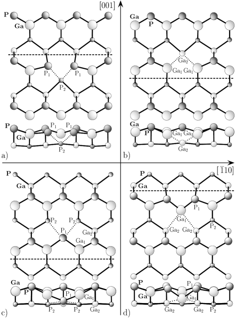
Let us now consider a gallium vacancy at the surface: Removing a cation from the surface layer results in creating dangling orbitals at the two neighboring phosphorus atoms at the surface and one at the neighboring atom in the second layer of the slab [Fig. 1(a)]. The phosphorus atoms in the first layer are twofold and the atom in the second layer is threefold coordinated. The calculated equilibrium positions are summarized in Table II. It is interesting to note that only the nearest neighbors around the defect significantly relax. All other atoms remain close to the positions of the unperturbed surface with a maximum relaxation smaller than Å. The relaxation of the nearest neighbors is characterized by a strong inward relaxation towards the vacancy. The atoms move inwards and lift the surface buckling locally almost completely. We also looked in detail for asymmetric distortions by starting from various low-symmetry configurations with equivalent k-point sampling. However, for neutral vacancies the energetically most stable structure maintains the symmetry of the (110) surface.
| (Å) | . | . | . | . | |||||
|---|---|---|---|---|---|---|---|---|---|
| (Å) | . | . | |||||||
| (Å) | . | . | . | . | |||||
| (Å) | . | . | . | . | |||||
| (deg.) | 90.1 | 93.1 | 120.3 | 98.6 | |||||
Due to the large relaxation of the phosphorus atoms towards the center of the vacancy, the distance between these atoms is strongly reduced. We find Å between and and Å for the separation, as compared to Å for the second nearest-neighbor distance in bulk GaP or Å in black phosphorus. [29] This indicates that the driving force behind the strong relaxation is the tendency to form phosphorus-phosphorus bonds. For the twofold-coordinated atoms we find a bond angle of , which is slightly closer to an ideal configuration than for the anions at the surface without a defect.
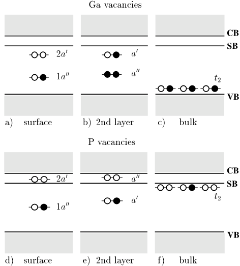
Figure 2(a) summarizes the results for the single-particle energies of the gallium surface vacancy. We find two defect-related states in the fundamental band gap: [30] One that we call is located eV above the valence band, the other called is close to the upper surface band. For the neutral charge state, is singly occupied and is empty. From analyzing the wave functions and the local density of states (LDOS), we find that both and consist mainly of -states centered at the three neighbors. From this analysis we find further a resonance at about eV also consisting mainly of -states centered at the three -neighbors. The lowest-lying localized level is determined at about eV and can be characterized as back bonds of the three nearest-neighbor atoms.
The symmetry and nature of these defect states can be qualitatively understood in terms of a simple model: [31] Creating a vacancy results in three dangling orbitals at the two surface atoms and at the atom in the second layer. Rehybridization of these orbitals will give rise to three nondegenerated defect states. According to the point symmetry of the (110) surface, these defect states are either symmetric or antisymmetric with respect to the mirror plane. This is different from the bulk system, where symmetry gives rise to and states formed by the dangling orbitals of four nearest-neighbor atoms. [32, 33] Analyzing the character of defect-related wave functions, we find the state to be symmetric while the singly occupied state is antisymmetric. The highest level is symmetric again.
To our knowledge this is the first ab initio calculation of cation surface vacancies. Allen, Sankey, and Dow [34] calculated the neutral gallium surface vacancy in an empirical tight-binding scheme: Neglecting atomic relaxations and electronic self-consistency, they found a singly occupied level eV above the valence-band maximum and an empty level at eV. These results contrast ours: Without including structural optimization, we find two nearly degenerate levels above the valence-band maximum, but upon atomic relaxation the levels split and take the energies shown in Fig. 2(a).
The electronic structure of surface defects can be investigated experimentally by scanning tunneling microscopy (STM) and scanning tunneling spectroscopy (STS). In STM, the charge states can be estimated by examining defects on - and -type doped crystals and comparing the local surface band bending caused by the charged defects with that of other charged impurities such as ionized dopants. [17] In STS, a tunneling spectrum at the defect site gives directly the position of ionization energies in the band gap as has been done for antisite defects at the GaAs (110) surface. [8] From our results, a first estimate of ionization energies of the defect can be obtained by the positions of the defect levels in the neutral charge state. As the gallium surface vacancy has a singly occupied state at midgap, we expect at least three charge states (). While we are not aware of STS measurements on surface vacancies, this result appears to be in contrast to STM measurements by Ebert, [35, 36] where the gallium surface vacancy was found to be neutral for both - and -type material. However, it is important to take into account that the charge state of a surface defect is not determined by the position of the bulk Fermi level but by the position of the surface Fermi energy. Indeed, photoelectron spectroscopy experiments [37] on GaP(110) indicate that the Fermi level at the surface is pinned near midgap, which might stabilize the neutral charge state. Further theoretical and experimental studies are necessary to clarify this issue.
B The phosphorus vacancy
The phosphorus surface vacancy, , is surrounded by three low-coordinated gallium atoms; two in the first layer () and one in the second layer (). The calculated equilibrium geometry of the defect is summarized in Table II and Fig. 1(b). As for the gallium vacancy, the equilibrium structure maintains the symmetry of the defect-free surface and atomic relaxations are mainly restricted to nearest-neighbor atoms. Second nearest neighbors relax less than Å. However, the inward relaxation of the surface atoms is clearly less pronounced than for the gallium vacancy. The origin of this is the different configuration of surface cations and anions on the defect-free surface: Since surface gallium atoms at the relaxed but unperturbed surface are located deeper in the surface than phosphorus atoms, the initial volume spanned by the nearest-neighbor atoms is much smaller for than for . As a consequence, the relaxation results in an increase of the surface buckling near the defect ( Å as compared to Å) and not in a decrease as for .
The distances between the atoms surrounding the defect are Å for the and Å for separation. This compares to Å in bulk GaP and Å in bulk gallium. [38] The angle between the back bonds of the surface gallium atoms is as compared to for the relaxed unperturbed surface. Thus, like the cations at the surface without a vacancy, the atoms prefer an bonding configuration. While this is the first ab initio calculation of anion surface vacancies at GaP (110), there have been several publications for anion vacancies at the (110) surface of GaAs: Calculating in a surface cell, Yi et al. [39] determined the height difference between surface gallium atoms for the neutral vacancy to be Å and for the negatively charged defect to be Å. Zhang and Zunger [40] calculated the inward relaxation of the atom towards to be Å and Å in the negative and positive charge state. The positively charged vacancy at GaAs (110) has also been calculated by Kim and Chelikowsky, [41] who give an inward relaxation of Å. Keeping in mind that GaP has a slightly smaller lattice constant than GaAs, these values are in close agreement with our result of Å.
The analysis of the electronic structure reveals also similarities between cation and anion surface vacancies. Again, we find two defect levels in the fundamental band gap [Fig. 2(d)]. The level is located 0.8 eV above the valence-band maximum and the level mixes with the unoccupied surface bands close to the conduction-band minimum. The occupation numbers are again one and zero for these defect states. In the valence band we find two localized states at about eV and eV. Since these are resonances in the valence band, they are not shown in Fig. 2(d). The levels and consist mainly of -states centered at the gallium neighbors, while the lower-lying resonance is mostly -like in character. As for , the energetically lowest level is symmetric with respect to the surface mirror plane, is antisymmetric, and is symmetric. The electronic structure of the anion surface vacancy has been previously calculated by Daw and Smith [42, 43] using a tight-binding method combined with Green’s-function techniques. Without considering atomic relaxations, they found the same sequence of electronic states for GaAs, [42] namely a symmetric level near the valence-band maximum and two levels in the band gap, where the lower, antisymmetric level is below midgap and the symmetric level is near the bottom of the conduction band. In the calculations for GaP, [43] the authors determined the position of the highest occupied level to be at eV, which is in good agreement with our value of eV for the unrelaxed surface vacancy. In contrast to these results, tight-binding calculations by Allen, Sankey, and Dow [34] predicted three deep levels at , , and eV.
Comparing our results with recent ab initio calculations for GaAs (110), we find qualitative agreement for the position and character of levels: Kim and Chelikowsky [41] obtained for the positively charged vacancy the same symmetry of the vacancy states and very similar positions of levels to those we find for the neutral vacancy at GaP (110). Yi et al. [39] determined the half-filled level above the center of the band gap while Zhang and Zunger [40] calculated this level to be and eV above the valence-band maximum for the positive and negative charge state.
Similar to the gallium surface vacancy, we expect also for the phosphorus surface vacancy at least two charge-transfer levels corresponding to the possible charge states (). This result is consistent with STM measurements by Ebert et al., [16, 35] who determined the phosphorus surface vacancy to be positively charged on -type material and neutral or negatively charged under -type conditions.
IV Subsurface vacancies
| Vacancy | Subsurface | Bulk | ||||||
| layer 1 | layer 2 | layer 3 | ||||||
| 7. | 0 | 2. | 1 | 4. | 5 | 3. | 8 | |
| . | 0 | 8. | 8 | 5. | 1 | 6. | 1 | |
Defects at and near the surface differ from their corresponding bulk defects due to changes in coordination number as well as in symmetry. In order to compare defects at different positions relative to the surface in a systematic way, we have calculated both types of vacancies in a bulk system as well as in the second and third layer of a surface cell. We will first focus on bulk defects and vacancies in the third layer. Vacancies in the second layer will be discussed separately: They exhibit features observed neither for bulk defects nor for surface defects.
A Bulk defects
Bulk vacancies in a zinc-blende semiconductor are characterized by a bonding level and a threefold-degenerate level . [32, 33, 44, 45, 46, 47, 48, 49, 50] For vacancies in the neutral charge state, the level lies in the valence band and the states are located above the valence-band maximum for the cation vacancy and near the conduction-band minimum for the anionic defect. Table III summarizes our results for structural changes and Figs. 2(c) and 2(f) show the position of levels for the relaxed defects. Atomic relaxation is mainly governed by an inward breathing relaxation conserving the tetrahedral symmetry of the lattice. We find the inward relaxation of the gallium vacancy to be 3.7% of the bulk bond distance ( Å). For the unrelaxed vacancy the resonance is located eV below the valence-band maximum as compared to eV calculated by Scheffler et al. [33] with a self-consistent pseudopotential Green’s-function method. The level lies at eV, in fair agreement with Ref. [33] ( eV). Allowing for atomic relaxation, the level shifts to eV while the level gains eV.
Calculating the atomic relaxations of , we find an inward relaxation of 6.1% (Table III). For the ideal atomic positions, the resonance is found at about eV below the valence-band maximum. Including atomic relaxations lowers the energy by eV. The level is found within the conduction band for the unrelaxed defect and lies below the band edge after relaxation.
An analysis of our bulk and slab calculations shows that these results are almost insensitive to whether the vacancies are in a bulk cell or in the third layer of a surface cell. Both the positions of the defect levels and and the formation energies (which will be discussed in Sec. V) agree well. The main differences are slight modifications in the atomic geometry. The origin of this is the changes in symmetry due to the presence of the surface (Table III).
B Defects in the second layer

| 0. | 47 | . | 06 | . | 10 | 0. | 21 | 0. | 09 | ||
| 0. | 09 | . | 03 | 0. | 02 | ||||||
| . | 70 | . | 03 | 0. | 08 | . | 40 | . | 03 | ||
| 1. | 76 | 0. | 11 | 0. | 13 | 0. | 45 | 0. | 10 | ||
| . | 58 | 0. | 01 | 0. | 02 | . | 41 | . | 05 | ||
| 0. | 06 | 0. | 21 | 0. | 02 | ||||||
| . | 85 | 0. | 03 | 0. | 02 | . | 28 | . | 05 | ||
| 1. | 03 | 0. | 07 | 0. | 03 | 0. | 54 | 0. | 07 | ||
Let us now focus on neutral vacancies in the second layer. The results for the equilibrium structure are summarized in Table IV and Figs. 1(c) and 1(d). As for surface vacancies, the atomic structure of cation and anion vacancies maintains the symmetry of the defect-free surface. Analyzing the atomic relaxations, we find significant displacements for the nearest-neighbor atom at the surface. For both defects this atom moves almost into the center of the vacancy. Therefore, vacancies in the second layer could also be considered as vacancy-antisite complexes ( - and - ). In contrast to previous calculations for bulk vacancies (e.g., and - in GaAs), [51, 52, 53] we do not find the second-layer subsurface vacancies to be metastable. Figure 3 shows the energy of the defects as a function of the -coordinate of the nearest-neighbor atom () at the surface. At this atom is confined to the plane of the surface anions (cations), and at it is placed in the plane of the cations (anions) in the second layer. In the equilibrium structure, we find the total displacement of the atom next to to be Å, and that of the atom next to is Å. These values can be compared to Å for the bond length between atoms in the first and second layer on the relaxed unperturbed surface. In contrast to the surface vacancies, we find a substantial displacement also for the second nearest-neighbor atoms in the surface layer. The two nearest-neighbor atoms in the second and the one in the third layer of the slab undergo almost no relaxation (Table IV).
The gallium vacancy has two levels within the fundamental band gap [Fig. 2(b)]: one doubly occupied at eV and one singly occupied at about eV. These states are antisymmetric and symmetric with respect to the surface mirror. For the phosphorus vacancy, we find a symmetric and singly occupied defect state at the middle of the band gap and an empty and antisymmetric state below the conduction-band minimum [Fig. 2(e)]. As for surface vacancies, we expect the cation and the anion vacancy in the second layer to show an amphoteric behavior: While under -type conditions they should act as a donor, -type conditions might stabilize a negatively charged state. Thus cation and anion vacancies in the first and second layer are possible candidates for pinning the surface Fermi level.
We conclude that the equilibrium structure of subsurface vacancies is mainly determined by the coordination of the nearest-neighbor atoms: Twofold-coordinated atoms in the surface layer can alter their position significantly without breaking the remaining bonds. However, threefold-coordinated atoms as completely surrounding a vacancy in the third or a deeper layer are strongly bound to their positions in the unperturbed lattice. Thus the ability of atoms in the second layer to relax is comparable to that of bulk atoms. Consequently, vacancies with only threefold neighbors (i.e., vacancies below the second layer) show very similar properties to bulk defects, while vacancies that have twofold-coordinated neighbors (i.e., vacancies at the surface and in the second layer) show a very different geometry and electronic structure.
V Defect formation energies
| surface | second layer | third layer | bulk | |
| unrelaxed | 0.99 | 1.06 | 1.06 | 1.02 |
| relaxed | 0.65 | 0.55 | 1.01 | 0.97 |
| surface | second layer | third layer | bulk | |
| unrelaxed | 1.05 | 1.05 | 1.08 | 1.09 |
| relaxed | 0.82 | 0.81 | 1.03 | 1.05 |
In the preceeding sections we have focused on the atomic geometry and the electronic structure of the defects, and how these properties are modified if a bulk defect is brought to the surface. We will now discuss how the energy required to create a vacancy in thermodynamic equilibrium (i.e., the formation energy) is affected by the surface. The formation energy of a defect is given by
| (1) |
and are the number of cations and anions with chemical potentials and , and is the number of excess electrons in exchange with the electron reservoir . Since we are focusing on neutral defects (), the formation energies are independent of the Fermi level. The Ga and P chemical potentials are related to each other by the condition of chemical equilibrium with the bulk GaP crystal:
| (2) |
The formation energy thus can be written as [47]
| (3) |
Moreover, we can approximate the upper limit of the chemical potential of each species by their corresponding bulk phases (). With the definition of the heat of formation of the crystal,
| (4) |
we get a range in which the chemical potential can be varied from gallium-rich to phosphorus-rich conditions:
| (5) |
Assuming metallic orthorhombic gallium [38, 54] and black phosphorus in an orthorhombic unit cell [29] to be the equilibrium structures of the condensed elemental phases, we get eV. This value is slightly higher than the experimental result ( eV). [55]
Figure 4 summarizes our results for the different relaxed defects. Over a wide range of the chemical potential, the anion surface vacancy is the energetically most favored defect. Only under very phosphorus-rich conditions is the cation surface vacancy preferred. Vacancies in the second and third layer show a significantly higher formation energy. Creating a gallium vacancy in the second layer takes eV more than at the surface while the other subsurface vacancies are even less favored.
Table V lists the formation energies with and without considering atomic relaxations. Note that all energies in Table V are given per broken bond and not per defect. This allows us to compare directly bulk and surface vacancies that have different coordinations. For simplicity, all formation energies are given under phosphorus-rich conditions. According to Eq. (3), the following discussion remains unaffected by considering a different chemical environment. Let us first discuss the case without any atomic relaxation: The most striking feature is the fact that the energy per broken bond is almost unchanged with respect to the position of the vacancy (surface, subsurface, bulk). [56] The deviations are smaller than eV, i.e., close to the estimated error of our method. The largest difference ( meV) is found for between the first and second surface layer.
However, if we consider atomic relaxation, the picture changes qualitatively: For vacancies in the first and second layer, we find a strong relaxation. Due to this relaxation the formation energy is largely reduced (up to eV, i.e., the energy gained by atomic relaxation is one order of magnitude larger than for bulk vacancies). It is further interesting to note that the relaxation energy for is about twice as large as for .
For bulk vacancies and vacancies in the third surface layer, the lowering of the formation energy due to atomic relaxation is small and almost independent of the type of defect. It has been shown in Sec. IV A that these defects are very similar with respect to defect levels and atomic equilibrium positions. The presence of the surface also induces differences in formation energy that are less than meV indicating the bulklike nature of the subsurface vacancies.

VI Simulation of STM images
A Method
For simulating STM images we employ the Tersoff-Hamann approach. [57, 58] In this approach the tunneling current is proportional to the local density of states at the tip position, , integrated over the interval between the Fermi surface and the applied bias :
| (6) |
A positive bias results in imaging the empty states in the specified energy range at position and negative bias in imaging the filled states. By mapping surfaces of constant an isocurrent picture can be simulated. Alternatively the integration might be evaluated for fixed tip height. Calculations of various reconstructed semiconductor surfaces [59, 60, 61, 62] as well as surfaces with impurities and adsorbates [40, 41, 63, 64] have proven this approach to be very useful for the interpretation of experimental results.

B Results
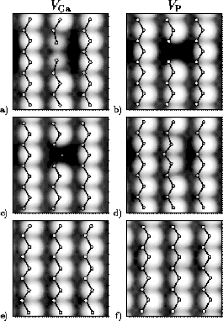
Figures 5(a) and 5(b) display our results for the occupied states of the gallium and phosphorus surface vacancy. The plots were taken at a distance of 3 Å from the outermost anion layer and include all occupied defect and surface states as well as surface resonances down to eV below the valence-band maximum. The pictures are dominated by the filled dangling bonds above the anions. Thus, for the defect-free surface the STM picture shows the periodicity of the surface lattice and the maxima of the charge density are close to the positions of the surface anions.
If we focus on the cation vacancy [Fig. 5(a)] we find a localized perturbation in the lattice: the dangling bonds of the two neighboring atoms along the direction are laterally displaced according to the relaxation of the atoms and clearly appear less intense than the ones farther away from the defect. This signature of the defect has also been identified in STM experiments. [35, 36] However, from the experimental data it is not clear whether this effect is due to atomic relaxation or due to changes in the electronic structure near the vacancy. We therefore compared the LDOS above the surface dangling bonds of the neighboring atoms with that of dangling bonds farther away from the defect. The results are shown in Fig. 6 together with an inset defining the lateral positions where the tip height has been varied. In the investigated interval above the surface we find an exponential decay of the density into the vacuum. The decay constants at the two maxima are virtually identical (). We therefore expect that in constant current STM the height difference between the two maxima is not a function of the tunneling current. From Fig. 6 we find this height difference to be Å, which is very close to the difference in the atomic structure ( Å, Table II). We note that the good agreement between the height corrugation in the electronic and atomic structure is related to the specific structure of the (110) surface and that of the defect: Both rehybridization and charge transfer for this system are small, and our STM simulation mainly shows the filled surface dangling bonds, which are not significantly changed by the presence of the vacancy. This is true even for nearest-neighbor atoms. We expect larger deviations for charged surface defects or for more complex systems where defect states are less localized or where rehybridization of atoms near the defect is more prominent.
The STM simulation of the anion surface vacancy is characterized by a depletion of the density of states due to the missing dangling bond [Fig. 5(b)]. The perturbation is very localized above the defect site and already the dangling bonds located at the second nearest neighbors are not influenced by the defect. This agrees well with experimental data for the neutral defect [16] and with the short-range character of the defect’s perturbation of the surface as discussed in Sec. III.
Simulating the vacancies in the second layer, we get the results shown in Figs. 5(c) and 5(d). Due to the large relaxation of the anion in the surface layer, the gallium vacancy displays features similar to the surface phosphorus vacancy: The phosphorus atom above the vacancy has no states within the simulated energy range at that location, which can be explained by the large vertical displacement of this atom. For the phosphorus vacancy the dangling bonds of the second nearest neighbors are slightly displaced and depressed. As for the cation surface vacancy, we analyzed this behavior as a function of the tip height. We find the height difference of the tip to be Å as compared to Å structural relaxation. Thus, also the signature of this vacancy is mainly governed by the relaxation of the surface atoms. We note that the STM simulations of the gallium surface vacancy [Fig. 5(a)] and of the phosphorus vacancy in the second layer [Fig. 5(d)] show a remarkable resemblance. The same holds for the anion surface vacancy [Fig. 5(b)] and the cation vacancy in the second layer [Fig. 5(c)]. Therefore, we expect these defects to be hardly discernible in STM measurements of the occupied states. However, for the gallium vacancy at the surface and in the second layer, the highest occupied defect state has a different symmetry [Figs. 2(a) and 2(e)]. Thus, both defects should be distinguishable in experiment. Also at the surface and in the second layer should be distinguishable in experiments such as scanning tunneling spectroscopy because they exhibit very different positions of the highest occupied defect state [Figs. 2(b) and 2(d)].
The simulation of a gallium vacancy in the third layer is virtually identical to that of a defect-free surface [Fig. 5(e)]. For the phosphorus vacancy, a slight depression above the missing atom is found [Fig. 5(f)], which, however, might be too weak to be resolved in experiment. We therefore expect that neutral vacancies below the second surface layer cannot be detected by STM measurements. For charged defects the local surface band bending induced by the impurity might change this result qualitatively. [5, 7]
VII Summary
Using first-principles total-energy calculations we investigated neutral surface and subsurface vacancies on both sublattices at GaP (110). Atomic relaxations, electronic structure, as well as formation energies were analyzed, and STM pictures of the various vacancies were simulated.
For both the gallium and the phosphorus surface vacancy, we find a pronounced inward relaxation of nearest neighbors into the defect. The electronic structure is characterized by a singly occupied deep level for and . Thus we expect them to be amphoteric, indicating that surface vacancies are electrically active and potentially a source of compensation. From the third surface layer on, the defects show essentially the same properties as bulk vacancies, namely a breathing-mode-like relaxation of the nearest-neighbor atoms and a triply degenerate acceptor () and donor level (), respectively. Vacancies in the second surface layer are found to be unstable against the formation of vacancy antisite complexes where the nearest-neighbor surface atom moves towards the vacancy site. For , the highest occupied level lies near the empty surface band while for it is found at a midgap position.
As can be expected from their lower coordination number, surface vacancies are energetically preferred as compared to subsurface and bulk vacancies. Our results show that, especially at and near the surface, the formation energy of defects is significantly affected by rather large atomic relaxations. For all vacancies with nearest-neighbor atoms in the surface layer we find relaxation energies that are at least six times higher than for defects with four threefold-coordinated nearest-neighbor atoms.
Our calculated STM images of the surface vacancies agree well with available experimental data. The comparison of the STM simulation with the atomic structure shows that neutral vacancies at this surface exhibit a close relation between atomic relaxation and height corrugation in the STM picture. To our knowledge, unlike charged subsurface defects, which have been frequently observed using STM, uncharged subsurface vacancies have not been reported by experimental groups so far. This is consistent with our results for vacancies from the third layer on, which exhibit virtually no interaction with the surface. However, vacancies in the second layer look like surface vacancies in our simulation. In experiment they might be discerned from surface vacancies by spectroscopic methods.
Acknowledgements.
The authors would like to thank Ph. Ebert for stimulating discussions and unpublished data. This work was supported by the Deutsche Forschungsgemeinschaft.REFERENCES
- [1] W. E. Spicer, P. W. Chye, P. R. Skeath, C. Y. Su, and I. Lindau, J. Vac. Sci. Technol. 16, 1422 (1979).
- [2] W. E. Spicer, I. Lindau, P. R. Skeath, C. Y. Su, and P. Chye, Phys. Rev. Lett. 44, 420 (1980).
- [3] W. Walukiewicz, J. Vac. Sci. Technol. B 5, 1062 (1987).
- [4] W. Walukiewicz, Appl. Phys. Lett. 54, 2094 (1989).
- [5] M. B. Johnson, O. Albrektsen, R. M. Feenstra, and H. W. M. Salemink, Appl. Phys. Lett. 63, 2923 (1993); Appl. Phys. Lett. 64, 1454(E) (1993).
- [6] J. F. Zheng, X. Liu, N. Newman, E. R. Weber, D. F. Ogletree, and M. Salmeron, Phys. Rev. Lett. 72, 1490 (1994).
- [7] C. Domke, Ph. Ebert, M. Heinrich, and K. Urban, Phys. Rev. B 54, 10 288 (1996).
- [8] R. M. Feenstra, J. M. Woodall, and G. D. Pettit, Phys. Rev. Lett. 71, 1176 (1993).
- [9] J. Gebauer, R. Krause-Rehberg, C. Domke, Ph. Ebert, and K. Urban, Phys. Rev. Lett. 78, 3334 (1997).
- [10] T. A. Kennedy, N. D. Wilsey, J. J. Krebs, and G. H. Stauss, Phys. Rev. Lett. 50, 1281 (1983).
- [11] K. Saarinen, S. Kuisma, P. Hautojärvi, C. Corbel, and C. LeBerre, Phys. Rev. Lett. 70, 2794 (1993).
- [12] T. Laine, K. Saarinen, J. Mäkinen, P. Hautojärvi, C. Corbel, L. N. Pfeiffer, and P. H. Citrin, Phys. Rev. B 54, R11 050 (1996).
- [13] G. Cox, K. H. Graf, D. Szynka, U. Poppe, and K. Urban, Vacuum 41, 591 (1990).
- [14] S. Gwo, A. R. Smith, and C. K. Shih, J. Vac. Sci. Technol. A 11, 1644 (1993).
- [15] G. Lengel, R. Wilkins, and M. Weimer, Phys. Rev. Lett. 72, 836 (1994).
- [16] Ph. Ebert, K. Urban, and M. G. Lagally, Phys. Rev. Lett. 72, 840 (1994).
- [17] K.-J. Chao, A. R. Smith, and C.-K. Shih, Phys. Rev. B 53, 6935 (1996).
- [18] D. M. Ceperley and B. J. Alder, Phys. Rev. Lett. 45, 566 (1980).
- [19] J. P. Perdew and A. Zunger, Phys. Rev. B 23, 5048 (1981).
- [20] M. Fuchs and M. Scheffler, Comput. Phys. Commun. (to be published).
- [21] J. Ihm, A. Zunger, and M. L. Cohen, J. Phys. C 12, 4409 (1979).
- [22] H. J. Monkhorst and J. D. Pack, Phys. Rev. B 13, 5188 (1976).
- [23] R. Poerschke and O. Madelung, Semiconductors; Group IV-Elements and III-V-Components, Data in Science and Technology (Springer, Berlin, 1991).
- [24] C. Filippi, D. J. Singh, and C. J. Umrigar, Phys. Rev. B 50, 14 947 (1994).
- [25] C. B. Duke, J. Vac. Sci. Technol. B 11, 1336 (1993).
- [26] J. L. A. Alves, J. Hebenstreit, and M. Scheffler, Phys. Rev. B 44, 6188 (1991).
- [27] J. E. Klepeis, C. Mailhiot, M. van Schilfgaarde, and M. Methfessel, J. Vac. Sci. Technol. B 11, 1463 (1993).
- [28] C. Mailhiot, C. B. Duke, and D. J. Chadi, Surf. Sci. 149, 366 (1985).
- [29] Gmelins Handbuch der anorganischen Chemie - Phosphor (Verlag Chemie, Weinheim, 1964), Vol. 16B.
- [30] Following the notation for the irreducible representation of the point group, we label the states () if they are symmetric (antisymmetric) with respect to the surface mirror plane.
- [31] W. A. Harrison, Electronic Structure and the Properties of Solids - The Physics of the Chemical Bond (Dover, New York, 1989).
- [32] G. B. Bachelet, G. A. Baraff, and M. Schlüter, Phys. Rev. B 24, 915 (1981).
- [33] M. Scheffler, S. T. Pantelides, N. O. Lipari, and J. Bernholc, Phys. Rev. Lett. 47, 413 (1981).
- [34] R. E. Allen, O. F. Sankey, and J. D. Dow, Surf. Sci. 168, 376 (1986).
- [35] Ph. Ebert, Quantitative Untersuchung von Defekten auf Oberflächen von III-V-Verbindungshalbleitern mit dem Rastertunnelmikroskop (Berichte des Forschungszentrums Jülich, Jülich, 1993).
- [36] Ph. Ebert and K. Urban, Phys. Rev. B (to be published).
- [37] M. Leblans, R. K. R. Thoma, J. L. LoPresti, M. Reichling, and R. T. Wiliams, in Optical Inorganic Dielectric Materials and Devices, SPIE - The International Society for Optical Engineering, edited by A. Krumins, D. K.Millers, A. Sternberg, and J. Spigulis (SPIE, Bellingham, 1996), p. 2.
- [38] Landolt-Börnstein, in Numerical Data and Functional Relationships in Science and Technology, New Series, edited by K. H. Hellwege and O. Madelung (Springer, Berlin, 1984).
- [39] J.-Y. Yi, J. S. Ha, S.-J. Park, and E.-H. Lee, Phys. Rev. B 51, 11 198 (1995).
- [40] S. B. Zhang and A. Zunger, Phys. Rev. Lett. 77, 119 (1996).
- [41] H. Kim and J. R. Chelikowsky, Phys. Rev. Lett. 77, 1063 (1996).
- [42] M. S. Daw and D. L. Smith, Phys. Rev. B 20, 5150 (1979).
- [43] M. S. Daw and D. L. Smith, Solid State Commun. 37, 205 (1981).
- [44] G. A. Baraff and M. Schlüter, Phys. Rev. Lett. 55, 1327 (1985).
- [45] M. Scheffler, J. Bernholc, N. O. Lipari, and S. T. Pantelides, Phys. Rev. B 29, 3269 (1984).
- [46] M. Scheffler and J. Da̧browski, Philos. Mag. A 58, 107 (1988).
- [47] U. Scherz and M. Scheffler, in Imperfections in III-V Materials, Semiconductors and Semimetals Vol. 38, edited by E. R. Weber (Academic Press, New York, 1993), Chap. 1 p. 1.
- [48] K. Laasonen, R. M. Nieminen, and M. J. Puska, Phys. Rev. B 45, 4122 (1992).
- [49] A. P. Seitsonen, R. Virkkunen, M. J. Puska, and R. M. Nieminen, Phys. Rev. B 49, 5253 (1994).
- [50] J. E. Northrup and S. B. Zhang, Phys. Rev. B 50, 4962 (1994).
- [51] G. A. Baraff and M. Schlüter, Phys. Rev. Lett. 55, 2340 (1985).
- [52] Y. Bar-Yam and J. D. Joannopoulos, Phys. Rev. Lett. 56, 1213 (1986).
- [53] M. Bockstedte and M. Scheffler, Z. Phys. Chem, Neue Folge 200, 195 (1997).
- [54] M. Bernasconi, G. L. Chiarotti, and E. Tosatti, Phys. Rev. B 52, 9988 (1995).
- [55] F. Bechstedt and R. Enderlein, Semiconductor Surfaces and Interfaces (Akademie Verlag, Berlin, 1988).
- [56] Note that the relative formation energy of cationic and anionic vacancies depends on chemical potential as illustrated in Fig. (4).
- [57] J. Bardeen, Phys. Rev. Lett. 6, 56 (1961).
- [58] J. Tersoff and D. R. Hamann, Phys. Rev. B 31, 805 (1985).
- [59] R. M. Feenstra, J. A. Stroscio, J. Tersoff, and A. P. Fein, Phys. Rev. Lett. 58, 1192 (1987).
- [60] J. H. Wilson, D. A. McInnes, J. Knall, A. P. Sutton, and J. B. Pethica, Ultramicroscopy 42–44, 801 (1992).
- [61] J. Da̧browski, H. J. Müssing, and G. Wolff, Surf. Sci. 331-333, 1022 (1995).
- [62] Ph. Ebert, B. Engels, P. Richard, K. Schröder, S. Blügel, C. Dohmke, M. Heinrich, and K. Urban, Phys. Rev. Lett. 77, 2997 (1996).
- [63] H. Lim, K. Cho, I. Park, and J. D. Joannopoulos, Phys. Rev. B 52, 17 231 (1995).
- [64] R. Capaz, K. Cho, and J. D. Joannopoulos, Phys. Rev. Lett. 75, 1811 (1995).