Reentrant behavior in the superconducting phase-dependent resistance
of a disordered two-dimensional electron gas
Abstract
We have investigated the bias-voltage dependence of the phase-dependent differential resistance of a disordered -shaped two-dimensional electron gas coupled to two superconducting terminals. The resistance oscillations first increase upon lowering the energy. For bias voltages below the Thouless energy, the resistance oscillations are suppressed and disappear almost completely at zero bias voltage. We find a qualitative agreement with the calculated reentrant behavior of the resistance and discuss quantitative deviations.
pacs:
74.50.+r, 74.25.-q, 73.23.-bOver the past years experimental and theoretical investigations have revealed how the resistance of a normal conductor () strongly coupled to a superconductor () is modified due to the superconducting proximity effect. At the interface electrons are converted in Andreev reflected holes incorporating the macroscopic phase of the superconductor. Superconducting correlation between electrons and holes penetrates a distance into the disordered normal conductor with diffusion constant , where denotes the relevant energy (maximum of temperature or bias voltage ). A striking prediction by Artemenko et al. [1] in 1979 was that the resistance of a disordered normal conductor at low energies () returns to its full normal-state resistance , despite the presence of superconducting correlation. Originally, this prediction was valid for short disordered normal conductors [length , with superconducting energy gap ]. Recently, its validity has been extended to long disordered normal conductors coupled to superconductors [2, 3, 4]. Theoretical analysis based on impurity-averaged Keldysh Green’s function techniques [2, 3] has shown that transport can be described by an effective diffusion constant, which depends on energy and position. At low and high energies this effective diffusion constant returns to , its value in the normal state, and for intermediate energies it is enhanced at position . Therefore, the reduction in resistance should vanish for both low and high energies and thus display a reentrant behavior. The maximum reduction depends on the particular shape of the normal conductor and occurs around an energy of a few times the Thouless energy .
Several experimental observations regarding the reentrance of the resistance have been reported using different geometries of the normal conductor. We have reported a suppression at low energies of the superconducting phase-dependent resistance of a -shaped two-dimensional electron gas (2DEG) coupled to two superconductors employing an Andreev interferometry technique [5]. In a cross-shaped 2DEG interferometer [6], we observed a similar behavior. Charlat et al. [7] have studied the magnetoresistance of a normal metal Aharonov-Bohm ring coupled to a single superconductor. Recently, they have also studied a single -shaped metal wire connected to a single superconductor [8]. Finally, Petrashov et al. [9] have observed a reentrant behavior in a cross-shaped normal metal interferometer. Note, however, that their interpretation is hindered by the presence of a circulating supercurrent [10], which drastically modifies both the magnitude of the superconducting phase-dependent resistance oscillations as well as its shape. In Ref. [6] we were able to conclude that the effect of a circulating supercurrent was negligible, which also holds for the -shaped 2DEG interferometer reported here.
So far the zero-energy limit where the resistance should return fully to has not been reached. The experiments [5, 8, 9] have only reported an increase in resistance at low energies of about 55% of the maximum reduction in resistance.
In this paper, we will report a reentrant behavior observed in the bias-voltage dependence of the resistance of a -shaped 2DEG coupled to two superconducting terminals. Around zero energy the resistance oscillations due to the superconducting phase are almost completely suppressed, confirming the theoretical predictions [1, 2, 3, 4]. We will compare our data with theoretically calculated resistances, which will highlight the consequences of using a low electron-density semiconductor instead of a normal metal.
We have reinvestigated the same devices ( and ) as studied in Ref. [5]. Instead of focussing on the sample-specific resistance oscillations in higher magnetic fields, we will focus on the energy dependence of the low magnetic field resistance oscillations. For this purpose, we have included additional filtering in the leads connected to the device at cryogenic temperatures [11].
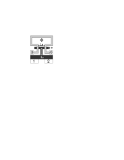
Our interferometer consists of a -shaped 2DEG attached to two superconducting terminals (see Fig. 1). These superconducting terminals (0) are the ends of an interrupted superconducting loop, which forces the electrochemical potential of the superconducting terminals to be equal. The superconducting phase difference , with , between both terminals can be varied linearly by an applied magnetic flux through this interrupted superconducting loop (area ).
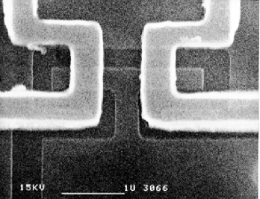
The -shaped 2DEG has been formed in an InAs/AlSb heterostructure, since highly transparent interfaces can be obtained between superconductors and the 2DEG in the underlying InAs layer. After removing the AlSb top layer, insulating trenches were defined in the InAs layer by wet chemical etching. Subsequently, 50 nm Nb superconducting electrodes were deposited after in situ Ar cleaning of the exposed InAs surface [12]. The transport properties of the InAs channel are roughly characterized by an electron density and an elastic mean free path m. The length of the vertical arm of the T-shaped 2DEG is m, the separation between both superconducting terminals is m, and the width of the horizontal arm is m.
The differential resistance is plotted versus applied magnetic field in Fig. 2. The period of the resistance oscillations corresponds with the expected flux quantum through the area of the interrupted Nb loop. The magnetic flux is not only present in this interrupted Nb loop, but also in the -shaped 2DEG itself. The additional phase-shifts due to this magnetic flux are expected to destroy superconducting correlations, and, consequently, the resistance oscillations when roughly one flux quantum penetrates the -shaped 2DEG (area 0.52 m2), which corresponds to about 50 G including a magnetic flux enlargement of about 1.7 due to the Meissner effect. For devices and the resistance oscillations disappeared around respectively 80 and 120 G, or equivalently an actual magnetic flux of about 1.6 and 2.4 .
We have investigated the energy dependence of the phase-dependent differential resistance by varying the applied dc bias voltage (see Fig. 2). Upon decreasing from 0.35 mV to 0.16 mV the magnitude of the resistance oscillations increases. The magnetoresistance oscillations plotted in the upper trace are almost disappeared, which was recorded when all relevant energies were smaller than : =0 mV and 0.02 meV.

The complete energy dependence of the magnitude of these resistance oscillations for device is collected in Fig. 3 (a). Note that the bias-voltage dependence directly reflects the energy dependence, whereas the temperature dependence corresponds to a convolution of the bias-voltage dependence with the Fermi-Dirac distribution. The oscillations appear below a dc bias voltage of about mV, which is well below the superconducting energy gap of 1.3 mV. The resistance oscillations reach a maximum magnitude around 0.1 mV, which is suppressed by about 80% at zero bias voltage. For comparison, we have plotted the bias-voltage dependence for the other device in Figs. 3 (b) and 3 (c). The data of Fig. 3 (c) are copied from Ref. [5] and were obtained without using cryogenic filtering. The main difference is visible around zero bias voltage, where the resistance oscillations are less suppressed due to an elevated noise temperature. However, the energy dependence of the resistance oscillations is qualitatively identical for both devices and displays the predicted reentrant behavior in the resistance.
The calculated energy dependence of the resistance for a -shaped interferometer is shown in Fig. 4. The length of the vertical and horizontal arms was assumed to be the same (==). The procedure is based on evaluating nonequilibrium quasiclassical Green’s functions for diffusive superconductors using the Keldysh technique. For detailed information about the calculations we refer to Ref. [2]. Here, we will only emphasize the assumptions which are made. First, the effective diffusion coefficient varies only in one dimension (along the wire length), transport is fully diffusive (), and phase-breaking events are neglected (). Second, the energy-dependent phase-shift during Andreev reflection is disregarded, which implies that all relevant energies () are assumed to be small compared to . Third, the pair potential in the normal conductor is neglected, which means that the electron-electron interaction strength is assumed to be zero.

In Fig. 3 (a) the resistance at =0 (solid line) describes the reentrant behavior of the resistance in zero magnetic field. The total resistance comprises the resistance of the vertical arm and the resistances of both horizontal arms in parallel. The small reduction in resistance at = (dashed line) below solely arises from the horizontal arms, which disappears when . In Fig. 3 (b) the magnitude of the resistance oscillations is plotted, which is the difference between the two curves of Fig. (3 (a). Figure 3 (b) also shows that the contribution of the vertical arm dominates over the contribution of both horizontal arms in parallel. The resistance oscillations are thus expected to have a maximum magnitude of about 18% around an energy .
Let us now proceed with a quantitative comparison between experiment and theory. The Thouless energy corresponding with the vertical arm of the -shaped 2DEG amounts to =0.06 meV for both devices, since the normal-state resistances are roughly identical. For devices and the maximum magnitude of the resistance oscillations are, respectively, about 0.5% and 2.2% of at an energy of 2.4 and 1.2. Although two nominally identical devices show a variation in both energy dependence and magnitude of the resistance oscillations, they do differ significantly from the theoretical expectation. In principle a nonideal -interface could be responsible for a reduction in magnitude. However, the interface resistance is small compared to the diffusive resistance of the -shaped 2DEG. In general the resistance at =0 is reduced below for , which implies that the probability for Andreev reflection dominates over normal reflection.

When we correct for the finite temperature in this experiment, the estimated magnitude of the resistance oscillations at zero bias voltage for device A will be slightly reduced and for device D will become negative. This nonzero magnitude at zero temperature and bias voltage results from the presence of sample-specific conductance fluctuations modulated by the superconducting phase [5, 6]. These oscillations are present at all energies and magnetic fields. Their rms magnitude is about 1 for device and 2 for device . The magnitude of the observed resistance oscillations at zero bias voltage is for both devices suppressed to this sample-specific magnitude. Therefore, we have confirmed the theoretical prediction [1, 2, 3, 4] that the nonsample-specific phase-dependent resistance vanishes at zero energy. Note that we have also reinvestigated the reentrant behavior in the two-terminal resistance of the cross-shaped 2DEG interferometer [6] using cryogenic filtering. Here, the oscillation magnitude around zero bias voltage was reduced by a factor of 2, which was limited by an enhanced magnitude of sample-specific oscillations due to an higher resistance of these devices.
Another contribution to the resistance oscillations at zero bias voltage could originate from the fact that our devices are not precisely diffusive, since . We can correct for that in the calculation by including a quantum point contact (QPC) with a resistance of about 350 in front of diffusive resistors modeling the -shaped 2DEG [13]. Note that this QPC resistance does not exhibit a reentrant behavior and is predicted to show phase-induced oscillations at zero energy [13]. We have calculated that for our geometry the expected magnitude for these QPC resistance oscillations should be less than 10% of the maximum resistance oscillations around 2.7. Therefore, we do not believe that for this device these QPC resistance oscillations could be responsible for a significant contribution to the observed oscillations around zero bias voltage [14].
So far we did not mention the energy dependence of the resistance at =0. Figure 2 shows that an increase in applied bias voltage causes a decrease in resistance. The resistance well above (bottom trace) does not show an increase, which seems to be in contrast with the reentrant behavior. However, a similar-sized 2DEG wire without superconducting terminals also shows an increase in resistance around zero bias voltage [15], which was attributed to be the Coulomb anomaly in the resistance caused by electron-electron interactions (EEI’s). Apparently, the contribution to the resistance caused by EEI’s masks the reentrant behavior in the resistance. An interesting remark is that EEI’s can give rise to a finite superconducting pair potential in the normal conductor, which can be modulated by the superconducting phase [2]. The resulting magnitude of the resistance oscillations depends on the strength of EEI’s and is in general much smaller compared to the reentrant behavior in the resistance. In this experiment, the magnitude of these resistance oscillations caused by EEI’s is smaller than the magnitude of the sample-specific oscillations.
The last issue we adress is the shape of the resistance oscillations, which for a slightly different geometry was predicted to develop a strong nonsinusoidal shape [2]. However, we observe only a very small contribution of higher harmonics. Around energies where the total magnitude exhibits a maximum the magnitude of the first higher harmonic (period ) is about 1.5 for device . For device we could not detect the second harmonic. Note that also Petrashov et al. [9] observed that the resistance oscillations are sinusoidal after correcting for the extrinsic deformation caused by the circulating supercurrent. Presently, we do not have a good understanding why certain geometries favor sinusoidal oscillations.
In conclusion, we have investigated in detail the reentrant behavior of the superconducting phase-dependent resistance of a -shaped 2DEG interferometer. The magnitude of the resistance oscillations at zero energy was shown to be suppressed to the magnitude of the phase-dependent sample-specific conductance fluctuations. The shape of the phase-dependent resistance strongly deviates from the theoretical predictions, which remains an open issue.
This work was part of the research program of the stichting voor Fundamenteel Onderzoek der Materie (FOM), which was financially supported by the Nederlandse organisatie voor Wetenschappelijk Onderzoek (NWO). B.J. van Wees acknowledges support from the Royal Dutch Academy of Sciences (KNAW).
REFERENCES
- [1] S.N. Artemenko, A.F. Volkov, and A.V. Zaitsev, Solid State Commun. 30, 771 (1979).
- [2] Y.V. Nazarov and T.H. Stoof, Phys. Rev. Lett. 76, 823 (1996); T.H. Stoof and Yu.V. Nazarov, Phys. Rev. B 53, 14 496 (1996).
- [3] A.F. Volkov, Phys. Lett. A 187, 404 (1994); S. Yip, Phys. Rev. B 52, 15 504 (1995); A.F. Volkov, N. Allsopp, and C.J. Lambert, J.Phys.:Condens. Matter 8, 45 (1996); A.A. Golubov, F.K. Wilhelm, and A.D. Zaikin, Phys. Rev. B. 55, 1123 (1997).
- [4] C.W.J. Beenakker, Phys. Rev B 46, 12 841 (1992); Y. Takane and H. Ebisawa, J. Phys. Soc. Jpn. 61, 2858 (1992); Y.V. Nazarov, Phys. Rev. Lett. 73, 1420 (1994); N. Argaman, Europhys. Lett. 38, 231 (1997).
- [5] S.G. den Hartog et al., Phys. Rev. Lett. 76, 4592 (1996).
- [6] S.G. den Hartog et al., Phys. Rev. Lett. 77, 4954 (1996).
- [7] P. Charlat et al., Phys. Rev. Lett. 77, 4950 (1996).
- [8] P. Charlat et al., Czech. J. Phys. 46, 3107 (1996).
- [9] V.T. Petrashov et al., JETP Lett. 64, 839 (1996).
- [10] B.J. van Wees, S.G. den Hartog, and A.F. Morpurgo, Phys. Rev. Lett. 76, 1402 (1996).
- [11] The present filtering setup contains in each lead a unit of three low-pass RC-filters attached to the mixing chamber of the dilution refrigerator, after which it passes a cylinder filled with Cu powder and is connected to the device: J.M. Martinis, M.H. Devoret, and J. Clarke, Phys. Rev. B 35, 4682 (1987).
- [12] P.H.C. Magnée et al., Phys. Rev. B 52, 11 630 (1995); P.H.C. Magnée et al., Appl. Phys. Lett. 67, 3569 (1995).
- [13] C.W.J. Beenakker and J.A. Melsen, Phys. Rev B 50, 2450 (1994); C.W.J. Beenakker, J.A. Melsen, and P.W. Brouwer, Phys. Rev. B 51, 13 883 (1995).
- [14] S.G. den Hartog et al., Phys. Rev. Lett. 79, 3250 (1997).
- [15] S.G. den Hartog et al., cond-mat/9710283.