Coulomb blockade effects in anodised niobium nanostructures
to be published in Supercond. Sci. Technol.)
Abstract
Niobium thin film wires were fabricated using electron beam lithography with a four layer liftoff mask system, and subsequently thinned by anodisation. The resistance along the wire was monitored in situ and trimmed by controlling the anodisation voltage. Depending on the room temperature sheet resistance, samples showed either superconducting or insulating behaviour at low temperatures. A Coulomb blockade was observed for samples exceeding 6 k per square. Samples were also made in a single electron transistor-like geometry with two weak links made by combined angular evaporation and anodisation. Their current-voltage characteristics could be modulated by a voltage applied to an overlapping gate.
1 Introduction
The properties of single electron devices [1] depend strongly on the electromagnetic environment [2, 3, 4]. Often it is important to bias the single electron device with a constant current rather than with a constant voltage, over a wide frequency range. This can in principle be achieved by isolating the device from the large capacitance of the biasing leads by closely surrounding it with high ohmic, low capacitance resistors [5]. Evaporated thin film alloy resistors [6] have the disadvantage of not allowing a tuning of the resistance in situ.
We have investigated a process where niobium wires were transformed to thin film resistors by anodisation [7, 8, 9]. The use of anodisation to tune metal film resistors has been mentioned first in 1959 [10]. Anodisation is frequently used to pattern prefabricated multilayers of niobium and barrier material for junction applications [11]. It has been used to weaken niobium strips into Josephson junctions [12], and to make variable thickness weak links in combination with a submicron sized anodisation mask [13]. Recently, prefabricated single electron transistors have been miniaturised by anodisation [14].
Ultrathin niobium films show transport properties typical for granular films [15]. In such systems, charging effects are expected to reduce the conductivity in the low bias region at low temperatures [16]. We have found experimentally that a Coulomb blockade occurs in samples that have been thinned sufficiently, and fabricated a device based on anodised niobium weak links that showed a modulation of current-voltage characteristics with an applied gate voltage. We refer to these samples as samples with two weak links in single electron transistor (SET)-like geometry.
2 Sample fabrication
2.1 Anodisation
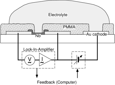
Figure 1 shows the experimental setup we used for the anodisation of microstructures. We spin coated the chip with a 1.8 m thick layer of PMMA and patterned it into an anodisation mask. Using e-beam lithography for this step provided precision alignment to the samples. Windows of about ten micrometre width were opened over the niobium strips that were to be anodised, and over a gold contact lead electrically isolated from the niobium pattern. This lead could then be used as cathode for the anodisation. Having such an integrated cathode near the chip centre reduced the amount of electrolyte needed to a small droplet of about 1 mm diameter, which minimised the risk for current leaks and made the handling of the chip much easier.
The design of the anodisation mask was chosen such that it could be used as a liftoff mask for the deposition of metal forming an overlapping gate electrode (for the samples in SET-like geometry).
As electrolyte, we used a mixture of 30.5 mmol ammonium pentaborate, 0.87 mol ethylene glycole and 2.22 mol water [17], which we found to work well at room temperature although it was originally intended for use at 120∘C.
To monitor the resistance of the sample during anodisation, we applied an AC excitation voltage with typical frequency kHz and amplitude mV and measured the resulting current with a lock-in amplifier. The voltage had to be kept small, and especially the DC component at zero, to avoid skewing the potential and thus the anodisation profile along the sample.
2.2 Resistance trimming
The formation of the anodic oxide film, and hence the increase of the sample resistance, is irreversible and could be controlled by regulating the cell voltage. Zeroing the voltage holds the resistance.
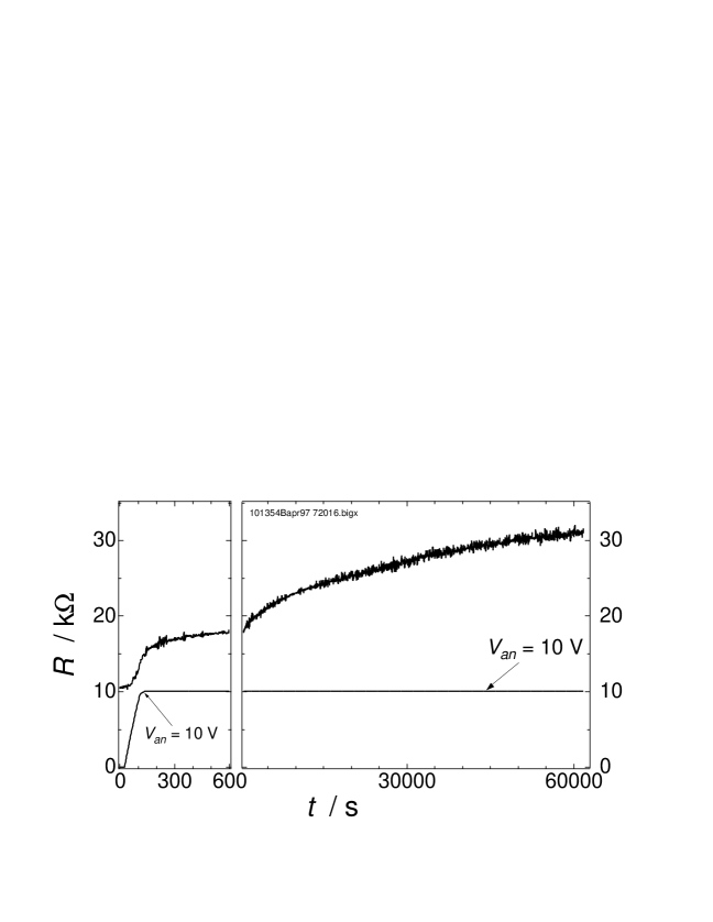
Since our anodised areas were very small, we did not attempt to anodise with a constant current. Instead, we adjusted the cell voltage and its ramping rate based on the reading of the sample resistance and its time derivative. Under such conditions, the oxide thickness is known to depend not only on the cell voltage, but also on time [18]; an estimation of the oxide film thickness from an ‘anodisation constant’ of 2.3 nm/V applicable under constant current conditions [19] is incorrect. Depending on the voltage ramping rate, our 20 nm thick films were anodised to practically infinite resistance at voltages between (15…25) V. The nonlinear behaviour of the oxide thickness is evident from figure 2. Here we quickly ramped the anodisation voltage up to 10 V and held it constant for more than sixteen hours. During this time, the resistance increased steadily. This behaviour can be exploited to achieve a precision in resistance trimming that is in principle only limited by the accuracy of the resistance measurement. We have tried different anodisation strategies and found that a total process time of a few hundred seconds gave the most stable and uniform samples, while providing sufficient trimming precision.
Our geometry for the resistor samples were strips about (120…180) nm wide and 10 m long, either individual or grouped as 120 m long wire equipped with equidistantly spaced leads allowing four probe measurements on each segment. The initially 20 nm thick Nb films had a sheet resistance of (50…120) , which by anodisation could be raised to several tens of kiloohms per square. Strips anodised simultaneously showed the same ratio between inital and final resistance within ten percent accuracy, up to sheet resistances of 20 k. For higher resistivities, the uniformity degraded, and at values of 40 k, similar strips could differ in resistance by a factor of 4 or more.
2.3 Patterning
The patterning of niobium with a lift-off process requires masks that can withstand the heat during the niobium deposition. Metal stencils supported by a sturdy polymer [20] have been reported as a suitable replacement for conventional all-polymer masks. We employed here a modification of a four layer resist [21] which had been used for the fabrication of Nb based single electron transistors. It consists of a PMMA top layer (50 nm), a germanium mask (20 nm) supported by hard baked photoresist (250 nm), and a PMMA bottom layer (50 nm) allowing liftoff. The top layer was patterned by electron beam lithography at 50 kV acceleration voltage and 20 pA beam current, and developed in a mixture of 400 mmol isopropanole and 170 mmol water. The pattern was then transferred to the Ge mask by rective ion etching (RIE) with carbon tetrafluoride CF4 as process gas. Subsequent RIE with oxygen through the photoresist and bottom PMMA layers gave the undercut profile and suspended bridges necessary for the angular evaporation technique. Etching times were estimated with some margin since we had no etch end detection.
The niobium was deposited in a multipurpose high vacuum system with an electron gun at a rate of (0.6…0.8) nm/s. The sample was neither cooled nor heated during evaporation, except by the evaporation itself. Due to the poor background pressure of Pa, the niobium had a residual resistance ratio of only 1.12 between room temperature and 4.2 K, and a superconducting transition temperature of the order of 1.5 K. With the same evaporation system and using a similar resist, Nb based single electron transistors had been fabricated earlier [21].
After the anodisation was completed, the samples were rinsed with deionised water. For the samples with two weak links in a SET-like geometry, a gate electrode of 50 nm gold was evaporated, and the mask removed prior to the low temperature measurements.
2.4 Angular evaporation
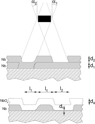
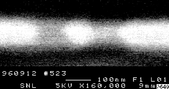
The shadow evaporation technique we used for the fabrication of samples with two weak links in SET geometry is shown schematically in figure 3. We evaporated two times 20 nm of Nb, tilting the sample to the substrate normal. Figure 4 is a scanning electron micrograph of a structure produced by this method, before anodisation.
Typical dimensions for these samples were line widths of (90…120) nm, length of the weak links nm and a length of the island separating these weak links nm. This method is capable of producing smaller islands than could be defined lithographically with similar processing. On the other hand, the symmetry of the two weak links depends on the equality in thickness of the two metal layers deposited in sequential evaporations. The film thicknesses were monitored with a water cooled crystal monitor. A reproducibility in thickness of about 10 % was estimated from control evaporations under similar conditions and stylus-method profilometry of the control samples.
3 Results
3.1 Resistor samples
Transport measurements were carried out in a dilution refrigerator at base temperature well below 50 mK. Details about the cryostat regarding the filtering of leads have been published elsewhere [22]. The bias voltage was applied symmetrically with respect to ground and fed to the sample via high ohmic bias resistors on top of the cryostat. The voltages over these resistors and over the sample were picked up by low noise amplifiers [23] and registered with digital voltmeters.

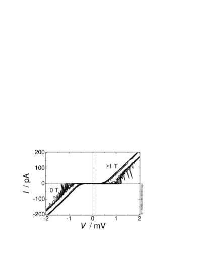
Figure 5 summarises the kinds of current-voltage characteristics (IVC) we observed in our resistor wire samples. Low resistive strips showed a remnant of a supercurrent (trace a). For higher (sheet) resistance, we observed a Coulomb blockade (trace b). Very high resistive samples showed not only a sharp threshold voltage, but a backbending IVC (trace c). Such a backbending is a characteristic of the Coulomb blockade of Cooper pair tunnelling [24] in arrays of Josephson junction arrays [25]. The backbending alone could be attributed to heating effects, but we also regularly observed a vivid switching of the IVC along the bias load line (figure 6, traces labelled ‘0 T’) that is typical in arrays of Josephson junctions [22]. This switching is random, but occurs between reproducible envelopes in subsequent sweeps. Further evidence for an influence of superconductivity on the IVC near the Coulomb blockade threshold threshold is the fact that a magnetic field suppressing superconductivity also suppresses the switching, as we see in figure 6.
To quantify the Coulomb blockade, we considered the offset voltage. Since the current-voltage characteristics were nonlinear over many decades in voltage, it was not enough to simply extrapolate the tangent to the IVC at the edges of the sweep range. Instead, we computed the local offset voltage [26] as the voltage value at the intersection of the tangent to the IVC in with the voltage axis,
| (1) |
Around zero bias, was approximately a linear function of . The extrapolation of to zero bias, , is a measure for the strength of the Coulomb blockade. For single ultrasmall junctions, this gives the Coulomb blockade in the global rule, where the whole electromagnetic environment influences the blockade.
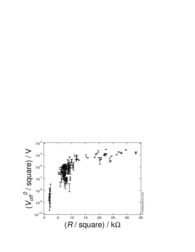
For 187 strips with lengths between ten and 120 m, we have measured the IVC without applied external magnetic field. The relation between and the sample resistance is shown in figure 7, where both quantities are normalised to the number of squares in the film and plotted against each other. The Coulomb blockade set in around a sheet resistance per square compatible with the quantum resistance
| (2) |
This supports the notion that there should be a universal sheet resistance for the superconductor-insulator transition in thin metallic films [27, 28].
3.2 Samples in SET-like geometry
Although our resistor wire samples showed a Coulomb blockade, we did not observe a modulation of the conductance with an applied gate voltage, as reported e. g. for high resistance In2O3-x wires [29]. We assume that the analogy between our wire samples and an array of junctions holds, and that the number of islands involved was so large that such effects averaged out below the measurement noise level.
Therefore, we fabricated the samples with two weak links and an overlapping gate described above, whose geometry resembles that of a single electron transistor (SET), where the oxide barriers have been replaced by short strips of niobium thinned by anodisation.
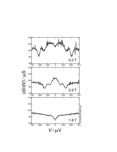
Samples that had a complicated current-voltage characteristic were susceptible to a modulation of this characteristic by a gate voltage. Figure 8 is a plot of the differential conductivity of such a sample as a function of bias voltage. The off-zero bias conductance peaks and dips moved towards zero bias with an increasing magnetic field and converged into a single conductance dip at an external field of 1.4 T. The latter zero bias conductivity dip is obviously indicating the Coulomb blockade of single electron tunnelling, while the off-zero bias structures are presumably caused by the superconducting gap. The reduction of the differential conductivity at zero bias in the field free case (top panel in figure 8) may be attributed to the Coulomb blockade of Cooper pairs [5].
On the other hand, samples that showed a Coulomb blockade with a very sharp threshold had current-voltage characteristics that could not be modulated with a gate voltage. Samples that had a very weak Coulomb blockade, resulting in a simple dip in the differential conductivity versus bias voltage characteristic around zero bias without further structure, were insensitive to a gate voltage as well. Scanning microscope inspection of these samples often suggested that the asymmetry between the two weak links was non-negligible.
To measure the response of the sample from figure 8 to the gate voltage, we quenched superconductivity by applying a field of 2 T, and biased the sample via high ohmic resistors at a series of practically constant drain-source currents. We then measured the drain-source voltage drop while sweeping the gate voltage up and down. Figure 9 gives the resulting control curves ( vs. at constant ).

The influence of the gate voltage is obvious for low drain-source currents (bottom panel). At other points along the - characteristic, namely for oppositely directed current, or higher current (top panel), the correlation between the control curves resulting from upward and downward sweep in gate voltage was less pronounced.
The large period of the observed sawtooth oscillations would correspond to a total island capacitance of only 3 aF, if one assumed that the sample acted as a single electron transistor. This capacitance estimate is unrealistically low. Control curves with such a large periodicity in gate voltage are, however, typical for systems of multiple tunnel junctions, e. g. those produced by the step-edge cutoff technique [30], or nanofabricated silicon wires [31].
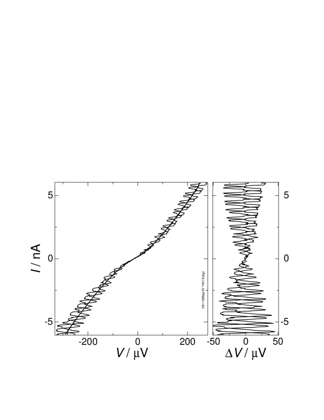
In another sample, we managed to modulate the drain-source current-voltage characteristic by applying a gate voltage. For the measurement shown in figure 10, we ramped the bias current up and down over one period with a frequency of 8 mHz. Simultaneously, a sine shaped gate voltage with an amplitude of 120 mV and a frequency of 322 mHz was applied. At this amplitude, the whole modulation range of the IVC was covered. The left panel of figure 10 shows the modulated and the unmodulated IVC for comparison, and the difference in drain-source voltage between unmodulated and modulated IVC is plotted in the right panel. Unfortunately, this sample was destroyed before we could map out the modulation range to higher drain-source voltages. At 50 mK and a gate voltage amplitude of 200 mV, the measured modulation of the IVC translates into an average transistor gain of about 1/700 at the edges of the measured bias region.
The voltage swing dropped to about one fourth when the temperature was raised from 50 mK to 1.1 K.
The insulation resistance between drain-source and gate was at least 30 G, our measurement limit, for gate voltages up to V. There, a measurable current flow through the gate set in, reaching about 5 nA at V.
4 Conclusion
We have demonstrated that anodic oxidation of nanofabricated niobium thin film wires can be used to produce resistors of several hundred kiloohms on a length of ten micrometres. This technique is intrinsically limited by the onset of a Coulomb blockade when the sheet resistance per square exceeds the quantum resistance 6 k. The anodised wires show transport properties typical of an array of ultrasmall Josephson junctions, where superconducting effects coexist with charging effects. The low temperature current-voltage characteristics of these samples show a superconductor-insulator transition where the degree of anodisation is the tuning parameter.
Placing short anodised areas with the aid of lithographic techniques, one can fabricate transistor-like samples whose current-voltage characteristics can be modulated by a gate voltage. More efforts are needed to further characterise the complex niobium-niobium oxides system created by anodisation and comprising the resistors and single electron transistor-like structures.
Acknowledgements
Samples were fabricated in the Swedish Nanometer Laboratory, Göteborg. T. H. gratefully acknowledges financial support by the German Academic Exchange Service trough HSP II. This research is part of ESPRIT project 9005 SETTRON. We were supported by Swedish NFR, TFR, the Wallenberg Foundation, and the Commission of the European Communities.
References
- [1] Edited by Hermann Grabert and Michel H. Devoret. Single Charge Tunneling. Coulomb Blockade Phenomena in Nanostructures, volume 294 of NATO ASI Series. (Plenum Press, New York, 1992). ISBN 0-306-44229-9.
- [2] P. Delsing, K. K. Likharev, L. S. Kuzmin and T. Claeson. Phys. Rev. Lett. 63, 1180–1183 (1989).
- [3] M. H. Devoret, D. Esteve, H. Grabert, G.-L. Ingold, H. Pothier and C. Urbina. Phys. Rev. Lett. 64, 1824–1827 (1990).
- [4] Gert-Ludwig Ingold and Yu. V. Nazarov. Charge Tunneling Rates in Ultrasmall Junctions. In Single Charge Tunneling. Coulomb Blockade Phenomena in Nanostructures, Edited by Hermann Grabert and Michel H. Devoret, volume 294 of NATO ASI Series, chapter 2, p. 21–107. Plenum Press, New York, 1992. ISBN 0-306-44229-9.
- [5] D. B. Haviland, L. S. Kuzmin, P. Delsing, K. K. Likharev and T. Claeson. Z. Phys. B – Condensed Matter 85, 339–347 (1991).
- [6] L. S. Kuzmin, Yu. V. Nazarov, D. B. Haviland, P. Delsing and T. Claeson. Phys. Rev. Lett. 67, 1161–1164 (1991).
- [7] Herman A. Johansen, George B. Adams, Jr. and Pierre Van Rysselberghe. J. Electrochem. Soc. 104, 339–346 (1957).
- [8] L. Young. Anodic Oxide Films. (Academic Press, London, 1961).
- [9] C. V. d’Alkaine, L. M. M. deSouza and C. F. Nart. Corrosion Science 34, 109–115 (1993).
- [10] Improvements in or relating to Electrical Resistance Elements. Patent Specification (Complete Specification) 896,071, The Patent Office, London. Filed 1960-09-22 (in the United States 1959-10-12), published 1962-05-09.
- [11] H. Kroger, L. N. Smith and D. W. Jillie. Appl. Phys. Lett. 39, 280–282 (1981).
- [12] Hiroshi Ohta, Mitsuhiro Takahata, Yasuharu Yamada and Yoshiaki Takahashi. Jap. J. Appl. Phys. 26, 1613–1614 (1987). Proc. 18th Int. Conf. on Low Temperature Physics, Kyoto, 1987.
- [13] Toshinari Goto. Jap. J. Appl. Phys. 20, L19–L21 (1981).
- [14] Y. Nakamura, D. L. Klein and J. S. Tsai. Appl. Phys. Lett. 68, 275–277 (1996).
- [15] S. Wolf and W. H. Lowrey. Phys. Rev. Lett. 39, 1038–1041 (1977).
- [16] C. J. Gorter. Physica 17, 777–780 (1951).
- [17] R. E. Joynson, C. A. Neugebauer and J. R. Rairden. J. Vac. Sci. Technol. 4, 171–178 (1967).
- [18] Y. L. Chiou. Thin Solid Films 8, R37–R39 (1971).
- [19] L. Young. Can. J. Chem. 38, 1141–1147 (1960).
- [20] A. K. Jain, J. E. Sauvageau, D. B. Schwartz, K. T. Springer and J. E. Lukens. IEEE Trans. Magnetics MAG-21, 955–958 (1985).
- [21] Y. Harada, D. B. Haviland, P. Delsing, C. D. Chen and T. Claeson. Appl. Phys. Lett. 65, 636–638 (1994).
- [22] D. B. Haviland, S. H. M. Persson, P. Delsing and C. D. Chen. J. Vac. Sci. Technol. A 14, 1839–1843 (1996).
- [23] Per Delsing. Single Electron Tunneling in Ultrasmall Tunnel Junctions. Ph.D. thesis, Department of Physics, Chalmers University of Technology, Göteborg, 1990. ISBN 91-7032-509-x.
- [24] L. J. Geerligs, M. Peters, L. E. M. de Groot, A. Verbruggen and J. E. Mooij. Phys. Rev. Lett. 63, 326–329 (1989).
- [25] C. D. Chen, P. Delsing, D. B. Haviland and T. Claeson. Physica Scripta T42, 182–188 (1992).
- [26] P. Wahlgren, P. Delsing and D. B. Haviland. Phys. Rev. B 52, R2293–R2296 (1995).
- [27] D. Belitz and T. R. Kirkpatrick. Rev. Mod. Phys. 66, 261–380 (1994).
- [28] Y. Liu, D. B. Haviland, B. Nease and A. M. Goldman. Phys. Rev. B 47, 5931–5946 (1993).
- [29] V. Chandrasekhar and R. A. Webb. J. Low Temp. Phys. 97, 9–54 (1994).
- [30] S. Altmeyer, B. Spangenberg and H. Kurz. Appl. Phys. Lett. 67, 569–571 (1995).
- [31] R. A. Smith and H. Ahmed. Gate controlled Coulomb blockade effects in the conduction of a silicon quantum wire. to appear in J. Appl. Phys. 81 (6), 15 March, 1997.