Mobility of dislocations in semiconductors
Atomic-scale calculations for the dynamics of the 900 partial glide dislocation in silicon are made using the effective-medium tight-binding theory. Kink formation and migration energies for the reconstructed partial dislocation are compared with experimental results for the mobility of this dislocation. The results confirm the theory that the partial moves in the dissociated state via the formation of stable kinks. The correlation between glide activation energy and band gap in semiconducting systems is discussed.
Metallic systems are often ductile even at low temperatures, which is due to the high mobility of dislocations in these systems. In semi-conducting systems, on the other hand, there are large Peierls barriers which must be overcome in order to move a dislocation and these materials therefore behave brittle. The low mobility of the dislocations is due to the electronic structure in the semiconducting systems, and a direct proportionality between the band gap and the dislocation glide activation energy has been observed. Another difference between the metallic and the semiconducting systems, is that in the diamond cubic lattice there are two distinct (1,1,1) glide planes, giving rise to two different sets of dislocations, called the glide set and the shuffle set. Figure 1 shows the position of the two different slip planes, and we see that while the glide plane breaks three nearest neighbour bonds per atom the shuffle plane only breaks one nearest neighbour bond per atom.
In this paper we will address the problem of which slip plane is important for dislocation glide in semiconductors. Our interest for this problem arose from a paper by Gilman, where he based on the empirical relation between the dislocation glide activation energy and the band gap, argues that the shuffle set is the relevant dislocations in semiconductors. However, this seems to contradict high resolution transmission electron microscopy images of dislocations in silicon, since these show dissociated dislocations and this is only consistent with models of glide dislocations.
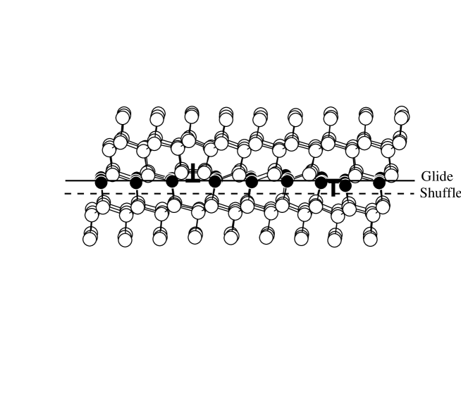
To investigate whether the mobilities of the glide dislocations are in accordance with experimentally observed dislocation mobilities in semiconductors, we have used the effective-medium tight-binding model(EMTB) to calculate the mobility of a particular glide dislocation, the 900 edge dislocation in silicon. The EMTB model is a total energy tight-binding method based on Effective-Medium Theory using a first-order Linear Muffin-Tin Orbital(LMTO) tight-binding model to calculate the band-structure energy. The model gives a quantum mechanical description of silicon and previous studies have demonstrated the ability of the model to accurately describe dislocations in silicon. For the atomic simulation we have used a atom unit cell containing two 900 partial edge dislocations with opposite Burgers vector (b=2.18Å), such that periodic boundary conditions can be used. Figure 1 shows a sideview of the unit cell, and Fig. 2(a) shows a top view of one of the partials. Note that the atoms in the core region(along the solid line) relax asymmetrically to obtain fourfold coordination. We find that this structure has an energy that is 0.18 eV/Å lower than a symmetric arrangement, where the atoms have “quasi fivefold” coordination, in good agreement with the ab initio result by Bigger et. al. of 0.2 eV/Å.
Dislocation glide is believed to proceed via the formation of stable kink pairs and their subsequent spreading along the dislocation line. At low stresses the velocity of the steady state motion of the dislocation is in this theory given by
| (1) |
where is the formation energy for a double kink, and is the migration energy.
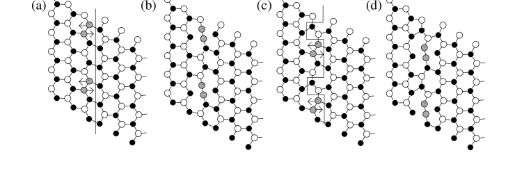
To find these energies we first create a kink by moving the shaded atoms in Fig. 2(a) in the direction of the arrows. The reaction coordinate is chosen as the difference between the coordinates of the two moving atoms in the direction of the arrows, and all other degrees of freedom in the unit cell is allowed to relax. The double kink of separation Å is shown in Fig. 2(c), and we find the formation energy to be eV. Standard elasticity theory predicts an elastic attraction between the kinks of eV at this separation, and we therefore estimate eV. Next we calculate the kink migration barrier, using the reaction path indicated by the arrows in Fig. 2(c). Figure 2(d) shows the transition state, and from the energy we find eV. The best experimental estimates give values eV and eV, and another tight-binding calculation by Nunes et. al. have found the values eV and eV. Our calculated migration barrier is in good agreement with these values, while the kink formation energy is too low. We believe that the latter is due to a strong attraction between the two kinks, which due to their close proximity is not described by elasticity theory. We also note that the atomic structure in the transition state is very similar to the symmetric reconstruction of the core structure, and from this analogy we estimate a barrier of eV in good agreement with the actual calculated value.
If we use the experimental value for the kink formation energy, we find an effective barrier for dislocation glide of eV, nearly twice the silicon bandgap ( eV). Since the same relation is found for other semiconductors it is tempting to search for a simple explanation for this proportionality. By inspecting our calculation we find that the main contribution to the migration barrier is from the one-electron term, i.e. the barrier is due to the electronic structure in the transition state. At the transition state there are states in the band gap(the same is the case for the symmetric reconstruction of the core structure,) and we therefore expect a proportionality between the bandgap and the migration barrier. Work is in progress to make a more quantitative model of the relation between the dislocation activation energy and bandgap of semiconductors.
In conclusion we have used the EMTB model to calculate the effective barrier for dislocation glide of the 900 partial in silicon. The calculated barrier is in good agreement with experimental findings, and we therefore conclude that the glide set is the relevant dislocations in silicon. Furthermore, inspection of the different contributions to the total energy suggests a proportionality between the semiconductor bandgap and the migration barrier of this dislocation, and the results might therefore have implications for other semiconductors as well.
References
References
- [1] J. J. Gilman, J. Appl. Phys 46, 5110 (1975).
- [2] J. J. Gilman, Science 261, 1436 (1993).
- [3] K. Stokbro, N. Chetty, K. W. Jacobsen, and J. K. Nørskov, Phys. Rev. B 50, 10727 (1994).
- [4] K. W. Jacobsen, J. K. Nørskov, and M. J. Puska, Phys. Rev. B 35, 7423 (1987).
- [5] O. K. Andersen, O. Jepsen, and M. Sob, in Electronic Bandstructure and its applications, Springer Lecture Notes, edited by M. Yussouff (Springer, Berlin, 1987).
- [6] L. B. Hansen et al., Phys. Rev. Lett. 75, 4444 (1995).
- [7] J. R. K. Bigger et al., Phys. Rev. Lett. 69, 2224 (1992).
- [8] J. P. Hirth and J. Lothe, Theory of Dislocations (Wiley, New York, 2nd edn., 1982).
- [9] H. Gottschalk et al., Phys. Stat. Sol. (a) 138, 547 (1993).
- [10] B. Y. Farber, Y. L. Iunin, and V. I. Nikitenko, Phys. Stat. Sol. (a) 97, 469 (1986).
- [11] R. W. Nunes, J. Bennetto, and D. Vanderbilt (unpublished).
- [12] J. C. Phillips, Bonds and Bands in Semiconductors (Academic Press, New York, 1973).
- [13] L. B. Hansen et al., (Work in Progress).