A New Class of Resonances at the Edge of the Two Dimensional Electron Gas
Abstract
We measure the frequency dependent capacitance of a gate covering the edge and part of a two-dimensional electron gas in the quantum Hall regime. In applying a positive gate bias, we create a metallic puddle under the gate surrounded by an insulating region. Charging of the puddle occurs via electron tunneling from a metallic edge channel. Analysis of the data allows direct extraction of this tunneling conductance. Novel conductance resonances appear as a function of gate bias. Samples with gates ranging from 1-170 m along the edge display strikingly similar resonance spectra. The data suggest the existence of unexpected structure, homogeneous over long length scales, at the sample edge.
pacs:
PACS 73.40.Gk, 73.40.HmRecieved
Edge states of the quantum Hall effect can be thought of as ideal channels that carry a net current only in one direction. Under conditions of the quantum Hall effect (QHE), the bulk of a two-dimensional electron gas (2DEG) is insulating, and gapless excitations appear only near the sample edges. The conductance associated with an edge state resulting from spin-split Landau level is precisely .[1] This result is true independent of the interactions between electrons and the details of the self- consistent potential which forms at the edge. However, interactions between electrons may lead to novel quantum phenomena reflected in the microscopic structure of the of the electron gas near the sample edges.
In a model including a self-consistent confining potential,[2, 3] the edge region breaks up into alternating sets of conducting strips which are the compressible EC and narrower insulating (rather incompressible) strips. This picture appears to be in reasonable qualitative agreement with recent experiments[4, 5, 6] under conditions of the integer QHE. However, it may miss important modifications that result from exchange[7, 8] and correlations.[9] More recent theoretical investigations have developed a significantly different picture when electron correlations are included. New effects such as spontaneous spin polarization[7] and edge reconstructions which develop abruptly with increasing magnetic field have been predicted.[8, 10]
While transport along the edge is rather insensitive to edge structure, transport across the edge is quite sensitive to it. Strong variations in this conductance arise from the presence of the incompressible strips (IS) separating EC associated with different Landau levels and the EC from the bulk. Prior investigations of the resistance of the edge incompressible strips were based mostly on the study of the non- equilibrium quasi-dc transport in 2DEG (for a review see Ref. [11]).
In this letter, we report an experiment which isolates the 2DEG edges and yields a powerful probe of their structure. A metallic island forms when the local 2DEG density is enhanced by adjusting the voltage on a gate covering the edge and part of a 2DEG. This island is spatially separated from a conducting edge and the bulk by a narrow (0.1 m wide) insulating strip. Using frequency dependent capacitance measurements, we probe equilibrium electron tunneling across the narrow quantum Hall insulator. This technique allows us to accurately measure resistances of the strip in the range of . As the gate bias is varied, we observe a series of sharp resonances in the tunneling conductance. This resonant structure is qualitatively indistinguishable for samples created using 1 m or 170 m long gates. We contend that these resonances arise from abrupt transitions in structure in or near edge incompressible strips. The sharpness of the resonances in the case of long gates indicates an unusual ubiquity of the transitions, despite the expected inhomogeneity of the sample edge.
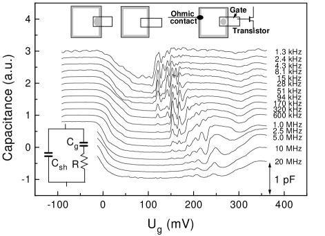
Five samples in the form of Hall bars defined by wet etching on a Al1-xGaxAs/GaAs wafer with mobility =700,000 cm2/Vs and concentration cm-2 were used for the measurements. The metal gate covering the edge of the Hall bar and part of the sample is depicted in the inset to Fig. 1. The gate dimensions (where is the length along the edge and is the width) were , , , , and for samples #1 through #5 respectively.
To measure the small capacitance between the 2DEG and the gate (geometrical values 3fF-1pF) in the frequency range Hz, an ac bridge scheme[12] is implemented. The input of a high electron mobility transistor is connected to the sample’s gate which forms the balancing point of the bridge. The circuit element consisting of the impedance between the 2DEG and the gate forms one arm of the bridge, and its value is precisely determined from the amplitude and the phase of a nulling ac voltage applied to a standard capacitor (10-100fF) connected as the bridge’s second arm.[12] Care was taken to set the measurement excitation level small enough (100 V) so that the data are observed to be amplitude independent. In addition, a dc gate voltage is applied to the gate through a 10M thin-film resistor. It allows us to vary electron density under the gate, with larger positive yielding larger .
In a first experiment we determine the impedance between the gate and the ohmic contact to the 2DEG as a function of in zero magnetic field. We model this impedance as a resistance in series with a capacitance between the gate and the 2DEG. A shunt parallel capacitance is included in the model (see bottom inset to Fig. 1). At low enough frequencies, becomes fully charged through during one cycle of the excitation. In this case, the measured impedance is a capacitance of value . When the 2DEG under the gate is fully depleted, this area no longer charges, and the measured impedance is just .
In magnetic field B the overall behavior becomes more complicated and interesting. First, we consider the case of integer Landau level filling factor in the bulk. Fig. 1 shows the dependence of the capacitance with the gate voltage at different frequencies for bulk filling factor in sample #1. The measured capacitance is large at small negative , and drops by an amount very nearly at small positive . It returns to the larger value at greater positive , albeit in a very nonmonotonic fashion. For higher frequencies, the capacitance minimum is widened, mostly from the high density (positive ) side.
The overall picture can be simply described as follows. The bulk of the 2DEG is effectively insulating at low temperature and, even for our lowest frequencies, charge cannot penetrate the bulk. Therefore, charge only appears in the compressible edge channel. Negative values of decrease the filling factor under the gate relative to the bulk value, and this conductive area merges with the edge channel (left inset to Fig. 1). Correspondingly, the measured capacitance is large in the whole frequency range. As is increased toward , the entire area under the gate, except that associated with edge channels, is insulating and the capacitance drops (middle inset). When exceeds , a conducting “puddle” of electrons in the next Landau level appears under the gate (right inset), but now this puddle is separated from the edge channel by an IS with filling factor . Electrons must tunnel across the IS to charge the puddle.[13]
The effective resistance of IS can be determined by fitting the frequency dependence of the capacitance to the model of the inset of Fig. 2. The capacitance has the form , where is the difference in the measured capacitance in the low and high frequency limits respectively. Fig. 1 thus demonstrates that conductance resonances give rise to the observed capacitance peaks.
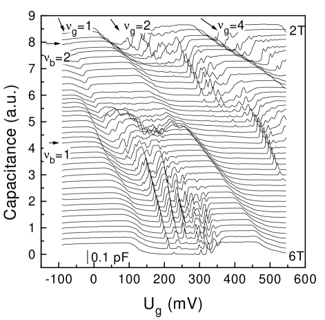
In Fig. 2, the capacitance of sample #2 at a frequency of 100 kHz is plotted as a function of for a range of B. Valleys clearly seen in the capacitance are associated with different integer (1,2,4). Let us follow the evolution of the valley around . At low B (2.5 T3.5 T), , and minima are seen only at , when part of the area under the gate is insulating. In the intermediate B region (3.5 T5 T) the bulk conducts poorly since . The situation is essentially the same as discussed for Fig. 1, and the mimima broaden on the side. For the largest fields (5 T6 T) shown in Fig. 2, the bulk is highly conducting, but now the conducting puddle under the gate with is separated from the bulk with and from the edge channel by an IS with . The other capacitance minima evolve in much the same fashion on the - B plane.
In Fig. 2, the same resonance structure seen in Fig. 1 can be followed over a wide range of B. We believe that these resonances arise from tunneling between the edge and the puddle. They persist even for B at which the bulk acts as an insulator. Additionally, a steeper density gradient on the side of the puddle nearest the edge leads to a narrower IS there than on the bulk side[2].
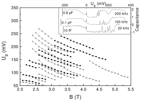
We have found striking similarity in the overall resonance structure in all of the investigated samples. This semblance is particularly manifest for resonances in the strip with . Fig. 3 shows the resonance positions detected on samples #1, #2, and #3. The positions are plotted as a function of the gate voltage, measured from the sharp structure observed on the low density side of the capacitance minimum (see the inset to Fig. 3.) Our lowest frequency measurements indicate that the sharp structure is immediately followed by the appearance of the compressible puddle under the gate. As the inset illustrates, smaller samples display a wider capacitance minimum, and the average conductance per unit gate length is smaller. Our technique is thus most sensitive in different regions of gate voltage for each sample. Nonetheless, there is no doubt that the resonances displayed in each sample arise from similar origins. An average spacing of 40 mV is clearly observed in each case. The strength and exact positions of the resonances change as any individual sample is thermally cycled to room temperature, but the qualitative features of the resonant structure (average spacings and resonance widths) remain.
Higher temperatures smear the resonances both by increasing the non-resonant background conductance and by broadening the resonances. The temperature dependence of one of the resonances, characteristic for all observed resonances for , is shown in the top inset to Fig. 4 for sample #3. The resonance broadens in an asymmetric fashion with increasing temperature, moving its center towards larger gate voltages, and the resonance width grows roughly linearly with the temperature.
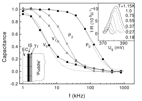
The detailed frequency dependence of the capacitance is different at resonance positions and between resonances. Fig. 4 shows the capacitance measured at a resonance peak () and at nearby valley () as a function of frequency together with the best fit by simple -model (dashed lines) as described above. While on resonance the experimental points are fit well with characteristic frequency 100kHz, the frequency dependence at the valley deviates significantly from the best fit with kHz at high frequencies. Such deviation is characteristic for all valleys.
To illustrate this point better and to exclude possible systematic error over any given frequency range, we also plot in Fig. 4 data for a different peak () and valley () chosen so that the corresponding characteristic frequencies are nearly the same. This deviation at the valleys indicates that a distributed resistance model should be used to fit the data rather than the simple form described above. The simplest form for this model includes two resistances: one associated with tunneling through the IS () and the other describing charge transfer through a transition region near the IS which separates it from the highly conducting interior of the puddle (see bottom inset to Fig. 4). Indeed, the shape of the experimental curves in the valleys is indicative of charging of two regions. One small region charges quickly, creating a high frequency tail, and a second region which is about 10 times larger charges more slowly. The curve is fit based on this model (see Fig. 4). The parameters inferred from the fit are and , where () is the resistance at the resonance .
Present models do not predict the observed resonant structure. According the electrostatic model of the edge developed by Chklovskii et al.[2] the width of the IS is a monotonically decreasing function of the density gradient. As the filling factor in the “puddle” increases beyond the integer value, the width of the strip and consequently the tunneling resistance must decrease.
One might consider the presence of favorably situated impurities as the origin of the tunneling resonances. Increasing the electron density under the gate causes the IS to move toward the edge. Even if the energy of an impurity state differs strongly from the Fermi energy, tunneling may be facilitated due to the presence of a virtual state each time the strip crosses the impurity location. Hence, each individual resonance trace could be assigned to a single “good” impurity. We find however that this portrait is inadequate to describe our results.
The data of Fig. 3 show that samples with vastly different dimensions show nearly identical resonances, strongly implying a common origin. It is very unlikely that in each case only one impurity is important over similar gate bias intervals. Most probably, impurity assisted tunneling averaged over many sites causes the growth of the non-resonant background with gate length.
The observed asymmetric growth of the resonances with increased temperature also discounts the impurity-assisted tunneling model. For resonant tunneling the conductance peak is expected to be both narrower and, in contrast to the observed behavior, higher with decreased temperature. For non-resonant impurity assisted tunneling, conductance peaks should remain unchanged at temperatures below the energy difference between the Fermi energy and the impurity energy level, whereas all observed resonances continue to narrow at the lowest experimental temperatures.
In our opinion, to account for the similarity of the resonances in the different samples it is necessary to assume that the tunneling conditions are modified homogeneously along the length of the strip. One possible origin of the resonances may be reconstruction of the electron gas at the edge due to the competition between the repulsive Coulomb interaction and the effectively attractive exchange interaction [8, 14, 15]. As of yet, there is no theory for these reconstructions in the “soft edge” regime of our samples. Another idea centers on the fact that the electron density across the IS is not perfectly constant. Nazarov[16] has predicted that such a density gradient may give rise to a crystalline ordering of electrons in regions in and adjoining the IS. We speculate that for gate biases off resonance, electrons in these regions are localized, impeding charge transfer to the puddle and leading to the charging process described in the bottom inset of Fig. 4. The positions of the resonances may correspond to particular density gradients at the location of the IS when one crystalline structure evolves into another, and regions adjoining the IS become more conductive.
Two basic facts are known about the resonances. One, they are no broader and appear no more frequently in large samples than small ones. This suggests a phenomenon occurring ubiquitously along the edge. Two, their exact positions and heights differ upon thermal cycling of samples and are therefore sensitive to the microscopic configuration of the sample. We conclude with the notion that these two facts are compatible only if a phenomenon exists which forces large regions of the edge to behave as a single structure.
We gratefully acknowledge helpful discussions with D.B. Chklovskii, B.I. Halperin, M.A. Kastner, A.H. MacDonald, K. Matveev, S. Simon, and X.-G. Wen and the assistance of H.B. Chan and D. Berman. This work is supported by the ONR, the Packard Foundation, and NSF DMR-9357226 and DMR- 9400415.
REFERENCES
- [1] B.I. Halperin, Phys. Rev. B. 25, 2185 (1982).
- [2] D.B. Chklovskii, B.I. Shklovskii, and L.I. Glazman, Phys. Rev. B. 46, 4026 (1992).
- [3] P.L. McEuen, et al., Phys. Rev. B. 45, 11419 (1992).
- [4] N.B. Zhitenev, et al., Phys. Rev. Lett. 71, 2292 (1993); Phys. Rev. B. 49, 7809 (1994).
- [5] S. Takaoka, et al., Phys. Rev. Lett. 72, 3080 (1994).
- [6] S.W. Hwang, D.C. Tsui, and M. Shayegan, Phys. Rev. B. 48, 8161 (1993).
- [7] J.G. Dempsey, B.Y.Gelfand, and B.I. Halperin, Phys. Rev. Lett. 70, 3639 (1993).
- [8] C.d.C. Chamon and X.G. Wen, Phys. Rev. B. 49, 8227 (1994); S.- R.E.M. Yang, A.H. MacDonald, and M.D. Johnson, Phys. Rev. Lett. 71, 3194 (1993).
- [9] L. Brey, Phys. Rev. B. 50, 11861 (1994); D.B. Chklovskii, Phys. Rev. B. 51, 9895 (1995).
- [10] H.A. Fertig, et al., Phys. Rev. Lett. 69, 816 (1992).
- [11] C.W.J. Beenakker and H. van Houten, Quantum Transport in Semiconductor Nanostructures (Academic, New-York, 1991).
- [12] R.C. Ashoori, et al., Phys. Rev. Lett. 68, 3088 (1992).
- [13] N.C. van der Vaart, et al., Phys. Rev. Lett. 73, 320 (1994).
- [14] O. Klein, et al., Phys. Rev. Lett. 74, 785 (1995).
- [15] R.C. Ashoori, Nature 379, 413 (1996). R.C. Ashoori, et al., Phys. Rev. Lett.71, 613 (1993).
- [16] Y.V. Nazarov, preprint cond-mat/9509133 (1995).