Resolution in Focused Electron- and Ion-Beam Induced Chemical Vapor Deposition
Abstract
The key physical processes governing resolution of focused electron-beam and ion-beam-assisted chemical vapor deposition are analyzed via an adsorption rate model. We quantify for the first time how the balance of molecule depletion and replenishment determines the resolution inside the locally irradiated area. Scaling laws are derived relating the resolution of the deposits to molecule dissociation, surface diffusion, adsorption, and desorption. Supporting results from deposition experiments with a copper metalorganic precursor gas on a silicon substrate are presented and discussed.
pacs:
Local electron-beam induced chemical vapor deposition (CVD) is a physical phenomenon well known from the build up of carbon contamination since the beginning of electron microscopy Oatley (1982). Recent research has spent tremendous efforts on the systematic creation of functional nanoscale deposits by means of focused electron beams and - with the development of scanning ion microscopes - of focused ion beams. Organic, organo-metallic, and inorganic precursor gas molecules were supplied into the microscope chamber. Upon irradiation, deposition results from non-volatile dissociation products whereas etching occurs when a reaction of dissociation products with the substrate leads to the formation of volatile species. These local deposition and etching techniques have numerous potential applications in nanosciences including fabrication of attachments in mechanics Yu et al. (2000), high-resolution sensors in magnetic, thermal, and optical scanning probe microscopy Utke et al. (2002); Edinger et al. (2000); Castagne et al. (1999), optical elements in nanooptics Sanchez et al. (2002); Nagata et al. (2005), contacts in electronics Gopal et al. (2004), and nanopores for ionic current measurements of cells and DNA in biology Nilsson et al. (2006); Danelon et al. (2006).
Few experiments analyze the physics of focused electron-beam (FEB) and focused ion-beam (FIB) induced deposition and etching. For FEB, Allen et al. Allen et al. (1988) noted that the spatial flux distribution of electrons passing through the adsorbed molecule layer consists of the incident primary beam (of up to several keV) and the emitted electrons: back scattered primaries and low-energy () secondary electrons. The entire energy spectrum is responsible for the dissociation process. For FIB, Dubner et al. Dubner and Wagner (1998) showed that this spectrum is associated to the energy deposited into the substrate surface through the collision cascade generated by the primary ion beam.
Our work is motivated by the fact that focused particle beam induced chemical vapor deposition and etching processes are widely used in nanoscale fabrication, but there are only very few attempts to describe the spatial resolution of this process theoretically. For a singular primary electron beam Silvis-Cividjian et al. Silvis-Cividjian et al. (2005) and Hagen et al. Hagen et al. (2006) concluded from Monte Carlo simulations that the ultimate resolution depends on the emitted secondary electron distribution. However, their assumption that the irradiated area is permanently covered with a monolayer of adsorbed molecules is idealized. In fact, as we will show, this coverage results from a balance of molecule depletion by dissociation and molecule replenishment strongly depending on adsorption, desorption, and diffusion. This is also White’s et al. conclusion White et al. (2006) who studied the gas transport phenomena at the microscope chamber scale affecting the overall deposition rate. Müller’s model Muller (1971) for FEB induced deposition, which was later adapted by Haraichi et al. Haraichi et al. (1993) to gas-assisted ion-beam induced etching, takes the key processes of surface diffusion, dissociation, desorption, and adsorption into account via an adsorption rate equation. However, he used a flat-top beam distribution which allows no conclusions about resolution.
In this letter we present an adsorption rate model without the above mentioned limitations, considering two relevant peak distributions for the incident beam and for the emitted spectrum, and a non-dissociative Langmuir adsorption term. It allows to derive two scaling laws for resolution and to estimate important physical parameters of the process. Finally, we discuss results of carefully designed experiments, clearly supporting the theoretical conclusions.
The model assumes second-order kinetics of molecule dissociation by electrons. In a system with rotational symmetry the vertical FEB deposition or etch rate (in units of dimension per unit time) as function of the distance from the centre of the primary electron (PE) beam is thus:
| (1) |
where is the volume of the decomposed molecule or etched atom, is the number of adsorbed molecules per surface unit, is the energy dependent electron impact dissociation cross section, is the energy of the PEs, and describes the spatial flux distribution of the electron energy spectrum generated by the PEs. Since the energy integral can be solved only approximatively due to missing data of adsorbed molecules and uncertain parameter estimates entering in the Monte Carlo simulation of the emitted electron distribution Allen et al. (1988), we use the simplified expression in Eq. 1, where represents an integrated value over the energy spectrum. Such cross sections were measured for several relevant molecules Kohlmannvonplaten et al. (1992); Scheuer et al. (1986); Kunze et al. (1967); Petzold and Heard (1991); Blauner et al. (1989); Lipp et al. (1996). The spatial distribution is a convolution of the Gaussian incident beam distribution with a peak function for the emitted spectrum which can be approximated by . Full widths at half maximum (FWHM) of the emitted distributions range between Hagen et al. (2006) and Allen et al. (1988). Similar considerations apply for FIB where the spatial distribution being responsible for molecule dissociation is a convolution of the primary beam distribution with the distribution of excited surface atoms generated by the collision cascade Dubner and Wagner (1998). Table 1 summarizes typical FWHM values of primary Gaussian beams.
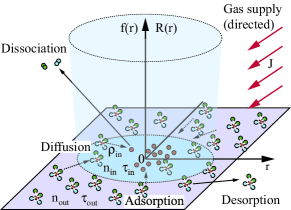
Four key processes as depicted in Fig. 1 are considered to determine the surface density of adsorbed molecules: a) adsorption from the gas phase governed by the precursor flux , the sticking probability , and coverage ; b) surface diffusion from the surrounding area to the irradiated area governed by the diffusion coefficient and the concentration gradient; c) desorption of physisorbed molecules after a residence time ; d) molecule dissociation governed by the product . For the molecule adsorption rate follows:
| (2) | |||||
The adsorption term in Eq. 2 describes a non-dissociative Langmuir adsorption, where is the maximum monolayer density given by the inverse of the molecule size. This adsorption type accounts for surface sites already occupied by non-dissociated precursor molecules and limits the coverage to . All parameters other than and are considered constant.
Solving eq. 2 for steady-state () and neglecting the diffusion term we obtain with the effective residence time of the molecules . The deposition or etch rate becomes
| (3) |
and represents the deposit or etch shape at a given time. For any peak function with a peak value , we can define the effective residence time in the center of the eletron beam and the effective residence time far away from the electron beam center . The dimensionless ratio represents a measure for depletion of precursor molecules due to dissociation at the center of the beam. With a Gaussian beam we derive the first scaling law of deposit size as function of depletion:
| (4) |
where and are the full widths at half maximum of and or, in other words, the FWHMs of the incident beam and the deposit. The idealized case of zero depletion, i.e. permanent monolayer coverage, corresponds to . Then deposition or etching proceeds in the electron-limited regime and the deposit (or etch) size corresponds to the electron beam distribution since the logarithmic term becomes 1. With increasing depletion the deposit (or etch) size becomes steadily larger than the beam size. For the peak function the expononent in eq. 4 becomes 1. The degree of depletion strongly depends on the dissociation frequencies summarized for FEB and FIB in Table 1. In order to replenish the dissociated molecules inside the continuously irradiated area by gas transport only, we need , i.e. the precursor supply frequency should exceed , being equivalent to (monolayers per second) for FEB. This corresponds to a precursor flux on the substrate of , setting and taking as typical value. For FIB several orders of magnitude larger gas supply would be needed. Desorption frequencies are situated around Edinger and Kraus (2000); Scheuer et al. (1986). Above estimations clearly suggest that most of the FEB and FIB processing experiments were performed in the precursor-limited regime limiting the minimum deposit or etch size.
| [1/nm2s] | [nm] | [nm2] | [1/s] | |
|---|---|---|---|---|
| FEB | ||||
| FIB | ||||
| 50 |
In the following we show under which conditions substantial replenishment by surface diffusion can be expected. Solving equation 2 numerically with MATLAB for steady-state (), the boundary conditions and , and with a Gaussian distribution we get and finally . A plot against the dimensionless variable for a given depletion and diffusive replenishment results in a unified representation of deposit shapes for any , see Fig. 2. Replenishment by diffusion is described by the dimensionless ratio , relating the diffusion path in the center of the beam with D being the diffusion coefficient, to the beam size. For , the flat top shape is defined by Eq. 3. With increasing diffusive replenishment deposits change into indented and round apex shapes, since adsorbed molecules increasingly reach the centre of the irradiated area before being dissociated. Hence both deposition rate and resolution increase. The maximum diffusion enhancement in deposition rate becomes at . For , Eq. 3 simplifies to since any depletion is entirely compensated by diffusion and a permanent monolayer coverage provided. In other words, the electron-limited regime is established and the deposit shape corresponds to the electron beam distribution .
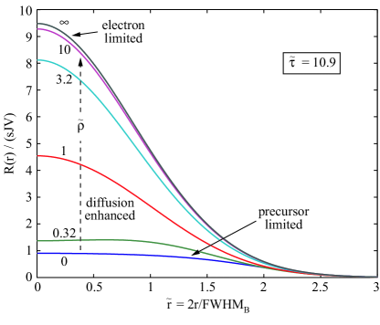
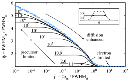
Figure 3 represents a graph relating the dimensioneless deposit size to irradiative depletion and diffusive replenishment. For any depletion with we get , i.e. the deposit size is within 3% close to when the related diffusion path inside the irradiated area becomes at least comparable to the size of the electron beam distribution. The deposits become broader than the electron beam for and small , branching out into constant maximum size given by Eq. 4 at negligible diffusive replenishment . Figure 3 holds independently of how diffusive replenishment is experimentally achieved: either via the beam size (using the focus of the beam) or via the diffusion path (changing precursor diffusion). The second scaling law of deposit size as function of diffusive replenishment is obtained as (circles in figure 3):
| (5) |
For the exponential peak function the expononent in Eq. 5 becomes again 1. Both Eq. 4 and Eq. 5 give upper limits for and . The smaller value of both defines the minimum deposit (or etch) size with respect to the beam size.
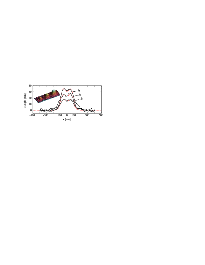
Now we present FEB deposit shape measurements obtained with a special designed SEM compatible atomic force microscope (AFM). The advantage is that AFM reveals three-dimensional topography features, like indented shapes, which are difficult to resolve in SEMs due to edge contrast effects. We used Cu(II)-hexafluoroacetylacetonate precursor molecules impinging on a native Silicon substrate with under irradiation with a 5 keV Gaussian electron beam ( and ). An indented shape with is observed, hence . Assuming and we get from Eq. 4 , i.e. . From Eq. 5 follows , i.e. . Using the relation for results in .
The values for the depletion, cross section, and diffusion coefficient represent lower limit estimations since the same FWHM-ratio can be obtained with larger depletion and larger diffusive replenishment, see figure 3. Taking as maximum dissociation cross section the molecule size Gromilov et al. (2004), we get . The corresponding upper limit estimate for the diffusion coefficient is derived from the shape fit in Fig. 4 to be .
Finally, we estimate diffusion coefficients needed for establishing the electron-limited regime under typical irradiation conditions summarized in table 1. Compensation of depletion by surface diffusion requires a beam focus smaller than the molecule diffusion path, , see figure 3. Together with the relation for we obtain for FEB and for FIB.
In conclusion, we quantified the crucial role of depletion and diffusive replenishment on deposit resolution for two relevant distributions: an incident Gaussian beam and an emitted distribution with exponential decay via an adsorption rate model. Our model is applicable to gas-assisted deposition and etching with focused electron- and ion beams and thus covers numerous applications in fundamental research and in nano-scale fabrication. We demonstrated how physical parameters can be determined from fitting experimental deposit shapes with our model. An extension of the studies to different beam shapes or experimental arrangements like pulsed beams at different temperatures is straightforward. It will enable the systematic determination of all physical key parameters involved in the process thus opening the door to the controlled fabrication of tailored nanoscale devices by charged particle beam induced CVD and etching.
We acknowledge financial support from the European Commission, FP6 Integrated Project NanoHand (IST-5-034274).
References
- Oatley (1982) C. V. Oatley, J Appl Phys 534, R1 (1982).
- Yu et al. (2000) M. F. Yu, O. Lourie, M. J. Dyer, K. Moloni, T. F. Kelly, and R. S. Ruoff, Science 287, 637 (2000).
- Utke et al. (2002) I. Utke, P. Hoffmann, R. Berger, and L. Scandella, Appl Phys Lett 80, 4792 (2002).
- Edinger et al. (2000) K. Edinger, T. Gotszalk, and I. Rangelow, J Vac Sci Technol B 19, 2856 (2001).
- Castagne et al. (1999) M. Castagne, M. Benfedda, S. Lahimer, P. Falgayrettes, J. P. Fillard, and Ultramicroscopy 76, 187 (1999).
- Sanchez et al. (2002) E. J. Sanchez, J. T. Krug, and X. S. Xie, Rev Sci Instrum 73, 3901 (2002).
- Nagata et al. (2005) T. Nagata, P. Ahmet, Y. Sakuma, T. Sekiguchi, and T. Chikyow, Appl Phys Lett 87 (2005).
- Gopal et al. (2004) V. Gopal, V. R. Radmilovic, C. Daraio, S. Jin, P. D. Yang, and E. A. Stach, Nano Lett 4, 2059 (2004).
- Nilsson et al. (2006) J. Nilsson, J. R. I. Lee, T. V. Ratto, and S. E. Letant, Adv Mater 18, 427 (2006).
- Danelon et al. (2006) C. Danelon, C. Santschi, J. Brugger, and H. Vogel, Langmuir 22, 10711 (2006).
- Allen et al. (1988) T. E. Allen, R. R. Kunz, and T. M. Mayer, J Vac Sci Technol B 6, 2057 (1988).
- Haraichi et al. (1993) S. Haraichi, and M. Komuro, Jpn J Appl Phys Part 1, 12, 6168 (1993).
- Silvis-Cividjian et al. (2005) N. Silvis-Cividjian, C. W. Hagen, and P. Kruit, J Appl Phys 98 (2005).
- Hagen et al. (2006) C. W. Hagen, N. Silvis-Cividjian, and P. Kruit, Scanning 28, 204 (2006).
- White et al. (2006) W. B. White, K. Rykaczewski, and A. G. Fedorov, Phys Rev Lett 97 , 086101 (2006).
- Muller (1971) K. H. Muller, Optik 33, 296 (1971).
- Dubner and Wagner (1998) A. D. Dubner and A. Wagner, J Vac Sci Technol B 7, 1950 (1998).
- Edinger and Kraus (2000) K. Edinger and T. Kraus, J Vac Sci Technol B 18, 3190 (2000).
- Scheuer et al. (1986) V. Scheuer, H. Koops, and T. Tschudi, Microelectron Eng 5, 423 (1986).
- Kohlmannvonplaten et al. (1992) K. T. Kohlmannvonplaten, L. M. Buchmann, H. C. Petzold, and W. H. Brunger, J Vac Sci Technol B 10, 2690 (1992).
- Kunze et al. (1967) D. Kunze, O. Peters, and G. Sauerbrey, Z Angew Physik 22, 69 (1967).
- Petzold and Heard (1991) H. C. Petzold and P. J. Heard, J Vac Sci Technol B 9, 2664 (1991).
- Blauner et al. (1989) P. G. Blauner, J. S. Ro, Y. Butt, and J. Melngailis, J Vac Sci Technol B 7, 609 (1989).
- Lipp et al. (1996) S. Lipp, L. Frey, C. Lehrer, B. Frank, E. Demm, S. Pauthner, and H. Ryssel, J Vac Sci Technol B 14, 3920 (1996).
- Gromilov et al. (2004) S. A. Gromilov, I. A. Baidina, P. A. Stabnikov, and G. V. Romanenko, J Struct Chem 45, 476 (2004).