Molecular Doping of Graphene
Graphene, a one-atom thick zero gap semiconductor Novoselov et al. (2004); Novoselov et al. (2005a), has been attracting an increasing interest due to its remarkable physical properties ranging from an electron spectrum resembling relativistic dynamics Novoselov et al. (2005b); Zhang et al. (2005); Gusynin and Sharapov (2005); Peres et al. (2006); Neto et al. (2006); Novoselov et al. (2006); Cheianov and Fal’ko (2006); Katsnelson (2006); Tworzydlo et al. (2006); Katsnelson et al. (2006) to ballistic transport under ambient conditions Novoselov et al. (2004); Novoselov et al. (2005a, b); Zhang et al. (2005). The latter makes graphene a promising material for future electronics and the recently demonstrated possibility of chemical doping without significant change in mobility has improved graphene’s prospects further Schedin et al. (2006). However, to find optimal dopants and, more generally, to progress towards graphene-based electronics requires understanding the physical mechanism behind the chemical doping, which has been lacking so far. Here, we present the first joint experimental and theoretical investigation of adsorbates on graphene. We elucidate a general relation between the doping strength and whether or not adsorbates have a magnetic moment: The paramagnetic single molecule is found to be a strong acceptor, whereas its diamagnetic dimer causes only weak doping. This effect is related to the peculiar density of states of graphene, which provides an ideal situation for model studies of doping effects in semiconductors. Furthermore, we explain recent results on its “chemical sensor” properties, in particular, the possibility to detect a single molecule Schedin et al. (2006).
Controlling the type and the concentration of charge carriers is at the heart of modern electronics: It is the ability of combining gate voltages and impurities for locally changing the density of electrons or holes that allows for the variety of nowadays available semiconductor based devices. However, the conventional Si-based electronics is expected to encounter fundamental limitations at the spatial scale below nm, according to the semiconductor industry roadmap, and this calls for novel materials that might substitute or complement Si. Being only one atomic layer thick, graphene exhibits ballistic transport on a submicron scale and can be doped heavily — either by gate voltages or molecular adsorbates — without significant loss of mobility Novoselov et al. (2004). In addition, later experiments Schedin et al. (2006) demonstrated its potential for solid state gas sensors and even the possibility of single molecule detection.
We show, that in graphene, aside from the donor-acceptor distinction, there are in general two different classes of dopants — paramagnetic and nonmagnetic. In contrast to ordinary semiconductors, the latter type of impurities act generally as rather weak dopants, whereas the paramagnetic impurities cause strong doping: Due to the linearly vanishing, electron-hole symmetric density of states (DOS) near the Dirac point of graphene, localised impurity states without spin polarisation are pinned to the centre of the pseudogap. Thus impurity states in graphene distinguish strongly from their counterparts in usual semiconductors, where the DOS in the valence and conduction bands are very different and impurity levels lie generally far away from the middle of the gap.
Impurity effects on the electronic structure of two-dimensional systems with Dirac spectrum were investigated in detail in connection with the problem of high-temperature superconductivity in copper-oxide compounds, and STM visualization of the order parameter around impurities is one of the most straightforward evidences of the -wave pairing in these systems Balatsky et al. (2006). For the case of a strong enough impurity potential, the formation of quasilocalized electron states in the pseudogap around the Dirac point is expected Balatsky et al. (2006), whereas a weak potential will not lead to the formation of quasilocalized states at all. This means that, in general, in this situation one can hardly expect a strong doping effect which requires existence of well-defined donor (or acceptor) levels several tenths of electron volt away from the Fermi level. However, if the impurity has a local magnetic moment its energy levels split more or less symmetrically by the Hund exchange, of the order of 1 eV, which provides exactly the situation favorable for a strong doping. To check this assumption we have chosen the system forming both paramagnetic single molecules and diamagnetic dimers . Note that magnetism of impurity atoms in graphene is interesting not only due to its effect on the electronic properties but also itself. As was shown recently Edwards and Katsnelson (2006) ferromagnetism based on spin polarization of -electrons in narrow impurity bands should be characterized by much higher Curie temperatures than typical for conventional magnetic semiconductors.
Doping and gas sensing effects in graphene related systems attracted a lot of research activity in the last years. Already the first experiments with graphene showed the possibility of inducing charge carriers to this material by the adsorption of various gases including , and Novoselov et al. (2004). Hall effect measurements proved, that induces electrons, whereas the latter two types of adsorbates result in holes as charge carriers. Furthermore, they showed that the detection of those gases at remarkably low concentrations or for even in the extreme limit of single molecules is possible Schedin et al. (2006).
Carbon nanotubes (CNT) being rolled up graphene sheets exhibit similar doping effects on gas exposure Kong et al. (2000) and stimulated first principles studies of these systems: DFT calculations for , and on nanotubes revealed possible physisorbed geometries on nondefective CNTs and developed a “standard model” to interpret this doping Peng and Cho (2000); Chang et al. (2001); Zhao et al. (2002): By considering of Mulliken or Löwdin charges of the adsorbed molecules, is found to accept 0.1 e- per molecule from the tube, whereas one molecule is predicted to donate between to e- Chang et al. (2001); Zhao et al. (2002). However, this “standard model” for CNTs fails for graphene, especially in explaining the qualitative difference between and the other adsorbates.
In this work we study the and adsorbate effects discussed above by combining ab-initio theory with transport measurements. Theoretically, the electronic properties of carbon related materials and the prediction of adsorbate geometries from first principles can be well addressed by the density functional theory (DFT). Although van der Waals forces are ill represented in the local density approximation (LDA) as well as in gradient corrected exchange correlation functionals (GGA) resulting in over- and underbonding, respectively Meijer and Sprik (1996), for polar molecules like these errors are of minor importance: In similar studies of on nanotubes both functionals yield qualitatively the same predictions of adsorption energies and geometries Yim et al. (2003). Here, we apply both functionals, so that we obtain upper and lower bounds for adsorption energies and related structural properties, such as the equilibrium distances between molecules and graphene plane.
All DFT calculations were carried out with the Vieanna Ab Initio Simulation Package (VASP) Kresse and Hafner (1994) using projector augmented waves (PAW) Kresse and Joubert (1999); Blöchl (1994) for describing the ion cores. The corresponding plane wave expansions of the Kohn-Sham orbitals were cut off at eV in the GGA Perdew (1991); Perdew et al. (1992) and at eV in the LDA-calculations. In this periodic scheme, single and adsorbates are modelled in and graphene supercells, respectively. The ionic configurations presented in this letter are fully relaxed, i.e. all forces being less than eV , and the convergence of subsequent total energy calculations is guaranteed by applying the tetrahedron method with Blöchl corrections on -centered k-meshes denser than , when folded back to the single graphene Brillouin zone.
In the spirit of Ref. Santucci et al. (2003), the DOS obtained in our DFT calculations are the central quantities in the following discussion of the adsorbate effects on the electronic properties of the graphene sheets. In particular, the occurrence of a strong acceptor level due to individual molecules is predicted in this way, as well as experimentally confirmed.
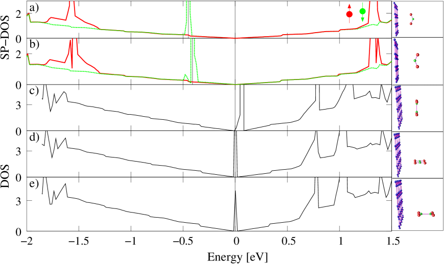
Gaseous stands in equilibrium with its dimer giving rise to various different adsorption mechanisms on graphene. For both, we obtained possible adsorption geometries as depicted in Fig. 1 right. The corresponding adsorption energies in GGA are meV (a), meV (b), meV (c), meV (d) and meV (e) per molecule with sheet-adsorbate distances of for the monomer and for the dimer. As usual, LDA yields higher adsorption energies - approximately meV for the monomer and meV for the dimer - and favours the adsorbates by nearer to the sheet.
The spin-polarized DOS of the supercells containing , shown in Fig. 1 a) and b), reveals a strong acceptor level at eV below the Dirac point due to these adsorbates in both adsorption geometries.
The molecular orbitals of correspond to flat bands and manifest themselves as peaks in the DOS. The energies of these peaks are virtually independent of the adsorbate orientation. Most important for doping effects is the partially occupied molecular orbital (POMO) of , which is split by a Hund like exchange interaction: The spin-up component of this orbital is approximately eV below the Dirac point and fully occupied, as it is also for the case of free molecule. The spin down component of the POMO is unoccupied for free , but eV below the Dirac point in the adsorbed configuration 111The energies of the POMO spin up and down orbitals relative to the Dirac points predicted by LDA are eV and eV, respectively, i.e. in almost quantitative agreement with the GGA results.. Hence, it can accept one electron from graphene.
In contrast to the paramagnetic monomer, the dimer, , has no unpaired electrons and is diamagnetic: on formation from two monomers the two POMOs hybridize. The resulting bonding orbital is the highest occupied molecular orbital (HOMO), whereas the antibonding combination forms the lowest unoccupied molecular orbital (LUMO) for free . The possibility of doping effects due to adsorbed dimers has been investigated using the DOS depicted in Fig. 1 c) - e).
Again, the molecular orbitals of the adsorbates are recognizable as sharp peaks in the supercell DOS. One finds that the HOMO is in all cases more than eV below the Fermi level and therefore does not give rise to any doping. However, the LUMO is always quite near to the Dirac point, i.e. between meV and meV above it 222LDA locates these LUMOs between meV and meV above the Dirac point..
These initially empty orbitals can be populated by the graphene electrons due to thermal excitations and act consequently as acceptor levels. Thus both, and , give rise to -type doping of graphene — with one decisive distinction: The affinity of the paramagnetic monomer to accept electrons from graphene is much stronger than for the dimer, manifesting itself in the energies of the acceptor levels being well below and near the Dirac point, respectively. This confirms exactly our estimations that magnetism is crucial for a strong doping effect. Without spin polarization, the quasilocalized states are typically formed in the pseudogap of the host DOS: The resonant energy of an impurity state is approximately located, where the real part of the denominator of the scattering -matrix vanishes Balatsky et al. (2006). Here, however, it is Hund exchange splitting which creates acceptor (or donor) peaks at distances of order of half of an eV which is optimal for strong doping, as we observed for the case of .
Experimentally, the existence of these two distinct types of impurity levels was confirmed by combining electric field effect and Hall measurements at different adsorbate concentrations. With the experimental setup described in Schedin et al. (2006) we measured the Hall resistance of an -exposed graphene sample as a function of the gate voltage , where different adsorbate concentrations are achieved by repeated annealing of the sample at K.
At magnetic fields T and room temperature K we obtained versus as depicted in Fig. 2. These measurements exhibit two characteristic features.
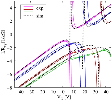
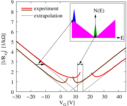
For gate voltages below V the curves are shifted in parallel towards lower values when increasing the absorbate concentration. Furthermore, the peak corresponding to is shifted to higher gate voltages, broadens and the minimal values increase with more adsorbates on the sheet. We argue that this behaviour, as a whole, is a direct evidence of the two distinct acceptor levels (See Fig. 3.).
Depending on the adsorbate concentration and the gate voltage there are in general three different types of charge carriers contributing to the Hall effect: electrons and holes in graphene as well as electrons in the impurity states. Assuming an equal electron and hole mobility in graphene, the inverse Hall resistance is given by , where () is the density of electrons (holes) in graphene, is the density of electrons in impurity states and their mobility in units of the graphene electron mobility.
We determined from our electric field effect measurements and the only adjustable is parameter density of impurity states yielding via the Fermi distribution. As the gate voltage is directly related to the total charge density of the sample , where the prefactor is determined by substrate properties as described in Novoselov et al. (2004), we can simulate the Hall resistance as a function of by assuming an explicit form of the impurity DOS.
It turns out, that for reasonable agreement of all experimental curves with the simulations has to be peaked around two distinct energies, meV and meV. Therefore, the experiment yields two types of acceptor levels, one rather close to the Dirac point and the other well below, in agreement with the DFT predictions. The simulations shown in Fig. 2 are according to these impurity level energies, in particular 333The broadness of the impurity levels does not strongly influence the simulations.. Fitting the number of impurity states () at meV ( meV) to each experimental curve yields the values for and depicted in Fig. 4.
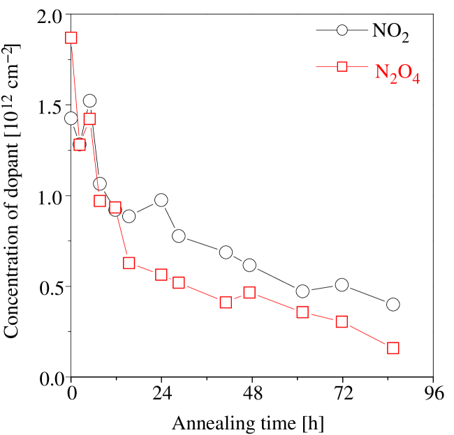
One sees that the adsorption of monomers and dimers is similarly likely, so that understanding the interplay of adsorbate and gate voltage effects on the transport properties of exposed graphene requires accounting for monomers as well as dimers. Note also, that the similar adsorption and annealing rates for and in experiment correspond nicely to the fact, that in both, GGA and LDA, the adsorption energies of the monomer are quite close to those of the dimer.
In conclusion, we have elucidated the microscopic origin of doping effects due to molecular adsorbates on graphene and work out the crucial relation between magnetic moments and doping strength in this context. In particular, we prove the occurrence of a strong acceptor level due to single molecules which is associated with the formation of local magnetic moment. Especially this strong acceptor level is the origin of many interesting phenomena and a promising candidate for tailoring the electronic and magnetic properties of future graphene devices. Besides explaining the effect of single molecule detection reported in Schedin et al. (2006) it is capable of controlling the occupancy of flat impurity bands in graphene near the Dirac point and can give rise to exchange scattering. This earns future attention, as it can result in strongly spin-polarized impurity states Wehling et al. (2006) and guides a possible pathway Edwards and Katsnelson (2006) to high temperature magnetic order in this material.
References
- Novoselov et al. (2004) K. S. Novoselov, A. K. Geim, S. V. Morozov, D. Jiang, Y. Zhang, S. V. Dubonos, I. V. Grigorieva, and A. A. Firsov, Science 306, 666 (2004).
- Novoselov et al. (2005a) K. S. Novoselov, D. Jiang, F. Schedin, T. J. Booth, V. V. Khotkevich, S. V. Morozov, and A. K. Geim, PNAS 102, 10451 (2005a).
- Novoselov et al. (2005b) K. S. Novoselov, A. K. Geim, S. V. Morozov, D. Jiang, M. I. Katsnelson, I. V. Grigorieva, S. V. Dubonos, and A. A. Firsov, Nature 438, 197 (2005b).
- Zhang et al. (2005) Y. Zhang, Y.-W. Tan, H. Stormer, and P. Kim, Nature 438, 201 (2005).
- Gusynin and Sharapov (2005) V. P. Gusynin and S. G. Sharapov, Phys. Rev. Lett. 95, 146801 (2005).
- Peres et al. (2006) N. M. R. Peres, F. Guinea, and A. H. C. Neto, Phys. Rev. B 73, 125411 (2006).
- Neto et al. (2006) A. H. C. Neto, F. Guinea, and N. M. R. Peres, Phys. Rev. B 73, 205408 (2006).
- Novoselov et al. (2006) K. S. Novoselov et al., Nature Phys. 2, 177 (2006).
- Cheianov and Fal’ko (2006) V. V. Cheianov and V. I. Fal’ko, Phys. Rev. B 74, 041403(R) (2006).
- Katsnelson (2006) M. I. Katsnelson, Eur. Phys. J. B 51, 157 (2006).
- Tworzydlo et al. (2006) J. Tworzydlo, B. Trauzettel, M. Titov, A. Rycerz, and C. W. J. Beenakker, Phys. Rev. Lett. 96, 246802 (2006).
- Katsnelson et al. (2006) M. I. Katsnelson, K. S. Novoselov, and A. K. Geim, Nature Phys. 2, 620 (2006).
- Schedin et al. (2006) F. Schedin, K. S. Novoselov, S. V. Morozov, D. Jiang, E. H. Hill, and A. K. Geim, Detection of individual molecules by graphene-based gas sensors (2006), cond-mat/0610809.
- Balatsky et al. (2006) A. V. Balatsky, I. Vekhter, and J.-X. Zhu, Rev. Mod. Phys. 78, 373 (2006).
- Edwards and Katsnelson (2006) D. M. Edwards and M. I. Katsnelson, J. Phys.: Condens. Matter 18, 7209 (2006).
- Kong et al. (2000) J. Kong, N. R. Franklin, C. W. Zhou, M. G. Chapline, S. Peng, K. J. Cho, and H. J. Dai, Science 287, 622 (2000).
- Peng and Cho (2000) S. Peng and K. Cho, Nanotechnology 11, 57 (2000).
- Chang et al. (2001) H. Chang, J. D. Lee, S. M. Lee, and Y. H. Lee, Appl. Phys. Lett. 79, 3863 (2001).
- Zhao et al. (2002) J. Zhao, A. Buldum, J. Han, and J. P. Lu, Nanotechnology 13, 195 (2002).
- Meijer and Sprik (1996) E. J. Meijer and M. Sprik, J. Chem. Phys. 105, 8684 (1996).
- Yim et al. (2003) W.-L. Yim, X. Gong, and Z.-F. Liu, J. Phys. Chem. B 107, 9363 (2003).
- Kresse and Hafner (1994) G. Kresse and J. Hafner, J. Phys.: Condes. Matter 6, 8245 (1994).
- Kresse and Joubert (1999) G. Kresse and D. Joubert, Phys. Rev. B 59, 1758 (1999).
- Blöchl (1994) P. E. Blöchl, Phys. Rev. B 50, 17953 (1994).
- Perdew (1991) J. P. Perdew, Electronic Structure of Solids ’91 (Akademie Verlag, Berlin, 1991).
- Perdew et al. (1992) J. P. Perdew, J. A. Chevary, S. H. Vosko, K. A. Jackson, M. R. Pederson, D. J. Singh, and C. Fiolhais, Phys. Rev. B 46, 6671 (1992).
- Santucci et al. (2003) S. Santucci, S. Picozzi, F. D. Gregorio, L. Lozzi, C. Cantalini, L. Valentini, J. M. Kenny, and B. Delley, J. Chem. Phys. 119, 10904 (2003).
- Wehling et al. (2006) T. O. Wehling, A. V. Balatsky, M. I. Katsnelson, A. I. Lichtenstein, K. Scharnberg, and R. Wiesendanger, Impurity states in graphene (2006), cond-mat/0609503.