Surface Spin-valve Effect
Abstract
We report an observation of spin-valve like hysteresis within a few atomic layers at a ferromagnetic interface. We use phonon spectroscopy of nanometer sized point contacts as an in-situ probe to study the mechanism of the effect. Distinct in energy phonon peaks for contacts with dissimilar nonmagnetic outer electrodes allow to localize the observed spin switching to the top or bottom interfaces for nanometer thin ferromagnetic layers. The mechanism consistent with our data is energetically distinct atomically thin surface spin layers that can form current or field driven surface spin-valves within a single ferromagnetic film.
pacs:
72.10.Di, 72.25Mk, 73.40JnSpin-valves in the current perpendicular to the plane geometry are usually nanopillars having two ferromagnets (F1 and F2) of different anisotropy, such that one is magnetically hard and the other is magnetically soft separated by a nonmagnetic spacer layer (N). The conductivity of such a spin-valve is governed by the giant magnetoresistance effect Fert ; Dieny and depends on the mutual orientation of the magnetization in F1 and F2 Katine (3). Recent studies have shown Meyers (4, 5, 6, 7) that nonmagnetic metal contacts to single ferromagnetic films (N-F) exhibit spin torque effects similar to those observed in F1/N/F2 spin-valves. For single N-F interfaces, non-hysteretic singularities of magnetic origin observed in the conductance are explained as arising from spin wave excitations in the ferromagnetic film Polianski (8, 9). Similar to the nanopillar case Katine (3), these peaks are observed only for one polarity of the bias current, namely for the electron current flowing from N into F, and their position on the current/voltage axis is proportional to the magnitude of the external magnetic field Ji (5, 6, 7). Another pronounced and rather unexpected feature of N-F nano-contacts, being the trade mark of the F1-N-F2 spin-valves, is hysteresis in resistance versus voltage, resulting in a bistable resistance state near zero bias. Its origin is under debate, with proposed interpretations ranging from surface exchange anisotropy Chen (10) and magneto-elastic anisotropy Kono (11) to spin vortex states ozy1 (12). In this work we investigate the mechanism of the hysteretic conductance in magnetic point contacts (PC’s) by combining PC phonon spectroscopy book (13) and magnetoconductance on the scale down to 1 nm in the contact radius, which is inaccessible by today’s lithographic means. We focus in particular on measuring thin films, where the magnetic film thickness () can be smaller than the PC diameter () and comparable or smaller than the ferromagnetic exchange length in the material. Such experimental configuration prevents formation of volume domains on the scale of the contact. Furthermore, we investigate the regime of dimensional cross over in vs. , the latter scale defining the contact core where the current density is maximum. In the limit both magnetic interfaces can be inside the high current density region and therefore actively contribute to spin transport, whereas for only one interface is expected to contribute to magnetoconductance. Such nanometer scale probing into the ferromagnetic surface, with an in-situ spectroscopic detection of the location of the nano-contact core, leads us to conclude that the observed magnetic effects are due to atomically thin surface spin layers acting as current or field driven spin-valves with respect to the magnetization in the interior of the ferromagnetic layer. Atomic scale domain walls of this kind have recently been shown to explain unusual surface magnetism in Co and Fe Gruyters (14, 15). The surface spin valve effects we report should be of quite general character, present in all spintronic devices provided the effect is not averaged out by interface imperfections on going from the nanometer scale to nanopillar structures of tens and hundreds of nanometers in size.
Our samples are Co films deposited onto oxidized Si substrates buffered with a non-magnetic bottom electrode (N2=Cu, Au) of 30 to 100 nm in thickness. The thickness of the Co films (F) ranged between 2 and 100 nm. For several samples the Co layer was capped with a 3 nm Au layer in order to prevent oxidation of the Co surface. The other non-magnetic electrode (N1=Cu, Ag, Au, W, Mo) is prepared in the form of a sharp tip, mechanically manipulated at low temperature to gently touch the F surface. All measurements are done at 4.2 K, with the samples always cooled from room temperature in zero field. The magnetic field is applied parallel to the film plane. For each contact a set of complementing transport characteristics were recorded: the differential resistance , magnetoresistance , and the so called PC spectrum, , provided the contact was mechanically stable for a sufficient period of time. Great many shorter lived contacts have been measured, resulting in a large library of still very informative subsets of magnetotransport data. The static resistance measured at low bias showed essentially the same behavior as the differential resistance. In the discussion to follow we therefore make no distinction between the two and restrict the data shown to .
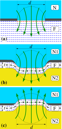
Three generic geometries of a point contact are illustrated in Fig. 1. Fig. 1a shows a schematic view of a nonmagnetic metal (N) in contact with a bulk or a thick film ferromagnet. The two metals are separated electrically except for a small circular orifice of diameter , the point contact size. This model corresponds to the experimental configuration studied previously Ji (5, 10, 7). In this case, only the upper interface between N and F is located in the region of high current density, hence only this interface plays a role in magneto-transport.
Fig. 1b illustrates the case where a thin F film is located in the lower half of the contact core (dashed circle). The upper F-N interface is located in the region of maximal current density and therefore contributes most to the spin torque effects. Notice that the contact core in this case is filled predominantly with N1 material, which therefore should dominate the PC spectrum. For a Co layer thinner than its contribution to the PC spectrum is expected to be small book (13). The Co phonon peaks are therefore not seen in the PC spectra discussed below.
A third characteristic, albeit less probable geometry is shown in Fig. 1c. Here, due to a supposed protrusion on the surface of N2, the Co nanolayer is elevated to the upper half of the contact core filled predominantly by N2, which therefore is expected to dominate the phonon PC spectrum. Consequently, the maximal current density is found at the bottom interface of the Co film. Thus, using PC phonon spectroscopy we can determine in-situ the relative weight of the two N/F interfaces in the magneto-transport for a given contact.
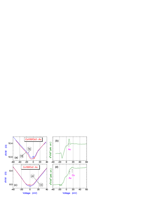
Fig. 2a illustrates the normal hysteresis for a hetero-contact Cu100/Co3-Au, a 100 nm Cu buffer electrode covered with a 3 nm thick Co film in contact with an Au tip. The higher resistance state is obtained for negative bias where the electrons flow from N1 to F. Cycling through a large positive bias (red curve), in this case approximately +40 mV, switches the contact into the low resistance state at about +10 mV. This state is preserved down to about -40 mV, followed by a smeared upward transition. Assuming the hysteresis is caused by a domain wall of type F1-DW-F2 within the Co layer, the large negative bias produces an anti-parallel (AP, or at least a large relative angle) configuration of the F1 and F2 magnetic sublayers, while for the large positive bias the spins in the two sublayers are parallel (P). The subsequently recorded PC spectrum shown in Fig. 2b, which is the measure of the electron-phonon interaction in the contact book (13), shows that the contact core is occupied predominantly by Au (N1). This means that the Co layer (whose phonon spectral lines are not detected owing to its small thickness) is located in the lower half of the PC core and, therefore, it is the upper N/F interface that plays the main role in the spin torque driven hysteresis.
The typical resistance of our contacts is , which correspond to the Sharvin diameter 10 nm. This is estimated as follows (see Fig. 3.9 and the accompanying text in book (13) for additional deatails):
which using the free electron approximation and the Fermi momentum yields
This value somewhat underestimates the true contact diameter since the Sharvin formula applies in the ballistic current regime. For the contacts reported herein the regime is closer to diffusive (the electron mean free path ), hence the typical contact diameter should be nm for . This means that for our nanometer thin ferromagnetic layers the condition is fulfilled for typical contacts, hence both ferromagnetic interfaces can be expected to contribute to magnetotransport, depending on the microscopic layout of the contact (see Fig. 1b,c).
Fig. 2c illustrates the case where the bottom interface is dominant, which leads to a reversal of the hysteresis in conductance. Such inverse or anomalous hysteresis is observed much less frequently owing to the fact that protrusive point contacts (see Fig. 1c) are less probable micromechanically. The outer electrodes were chosen with an aim to separate their main phonon peaks, which in the case of Cu and Au are found at approximately 17 and 10 mV, respectively book (13). The separation of 7 mV is large enough to reliably distinguish the peaks even for non-ballistic contacts with smeared phonon maxima Yanson (7). The dominant Cu maximum in Fig. 2d, in contrast to the spectrum of Fig. 2b, indicates that it is the bottom Co/Cu interface region that plays the main role in the electron and spin transport for this nano-contact. The corresponding hysteresis is anomalous, i.e., the large resistance state corresponds to the electrons flowing from the film into the tip (Fig. 2c). The spectroscopic data provides a natural explanation, namely, the contact core of highest current density is at the bottom F/N interface where the electrons flow from the Cu bottom electrode into Co. The transition to the high resistance state occurs above +35 mV and the reverse transition at -8 mV.
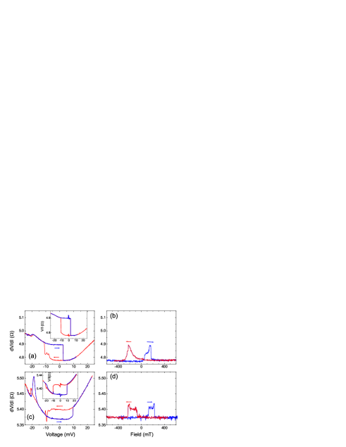
Fig. 3 illustrates the normal (a) and inverse (c) hysteresis in accompanied by a spin-valve like hysteresis in (b,d) for Cu30/Co5-Ag contacts. Here the switching AP-to-P and P-to-AP occur as sharp steps in resistance, occurring under the influence of a nominally unpolarized current (insets a and c) or an externally applied magnetic field. Importantly, the resistance difference between the stable at zero bias AP and P states is the same for the current and field induced transitions, even though the mechanisms leading to hysteresis are different in the two cases. For the bi-stability is caused by spin transfer torques while for with the external magnetic field parallel to the film plane the behavior is identical to the nano-pillar spin-valve magnetoresistance. This observation is true even for curves with smooth transitions such as Fig. 2a,c - the difference in resistance versus current and that versus field are the same. Notice also the maxima in at approximately mV, which are due to non-hysteretic magnetization excitations Ji (5, 7, 8).
Another important observation, based on our measurements of about one hundred contacts with hysteresis, is that statistically shows no trend as a function of the thickness of the Co layer in the range 2-100 nm, as illustrated in Fig. 4a, strongly suggesting that the observed hysteresis is a surface effect. As shown in Figs. 2,3,4b this surface effect can occur at either of the ferromagnetic interface and is indistinguishable in its current and field driven behavior from the standard three-layer spin-valve effect.
The above clear correlation between the dominant phonon maxima and the sign of hysteresis in the conductance of the hetero-contacts is straightforward conceptually, and reflects the limiting cases of the ferromagnetic layer being at the bottom or top of the contact core. Naturally, a richer behavior should be expected for very thin magnetic layers located symmetrically in the PC core. Namely, the spin torque effects from the two interfaces should superpose. An example of such behavior is shown in Fig. 4b. Here the polarity of the hysteresis near zero bias is normal, correlating well with the pronounced Au phonon maximum at 10 mV. At positive bias, expected to drive the contact into a low resistance state if one considers the top interface only, such a normal hysteresis transition indeed occurs at 15 mV. However, the presence of the bottom interface within the contact core, as evidenced by the Cu-phonon maximum in the PC spectrum, results in a superposed anomalous hysteresis at large positive bias. The resulting structure of the ferromagnetic layer of only 2 nm in thickness is a rather surprising double spin-valve of type or . The data in Fig. 2,3 with hysteresis of one type only represent therefore the limiting cases where the PC conductance is dominated by either one of the two N/F interfaces.
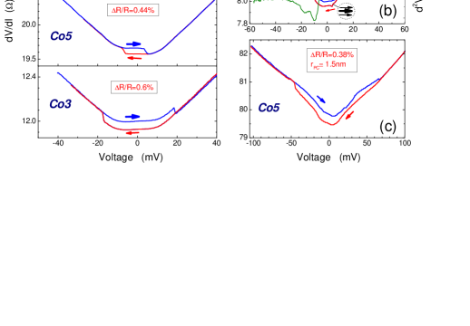
The contact core, dominating the charge and spin current in PC’s, approaches 1 nm scale for highly resistive contacts with . for such a contact, exhibiting a pronounced current driven hysteresis, is shown in Fig. 4c for a 5 nm thick Co layer. We estimate the radius of this contact core to be nm. Therefore the whole F1-DW-F2 magnetic sub-layer structure producing the hysteretic switching must be limited in thickness to some 3-4 atomic unit cells at the interface, which provides a decisive evidence that the surface spin layer acting as the “free” layer is atomically thin. This consideration and the lateral extent of the contact of only 3 nm (to an exchange-length thin ferromagnetic film) disqualifies any interpretation of the phenomenon based on volume like domains or vortex states. In particular, vortex states that are possible to produce in nm ferromagnetic particles in nanopillars should be unstable for contacts to continuous films studied here, especially at zero bias where circular Oersted fields are absent. We therefore rule out the vortex interpretation for our contacts, which are one to two orders of magnitude smaller than typical magnetic nanopillars.
The previously proposed interpretation Chen (10) of the normal hysteresis as due to a surface exchange bias in naturally oxidized Co films is faced with difficulties as well. First of all, making a true metallic contact removes any oxide from the contact region. Furthermore, in contrast to Chen (10) all our measurements are done on samples cooled in zero field, which we find does not diminish the hysteresis effects. As shown in Fig. 4b hysteresis is also observed in contacts to ferromagnetic films capped with protective Au anti-oxidation layers (we have measured a number of such contacts). As shown in Fig. 2,3,4b we also detect hysteresis due to the bottom ferromagnetic interface, which is produced in high vacuum and is certainly free from any oxide. Finally, surface exchange anisotropy anyway necessitates postulating a volume like domain Chen (10), which can be excluded for our nano-contacts to nanometer thin films. We therefore can rule out this mechanism for the effects we observe. It is important to mention that we observe pronounced magnetic hysteresis effects on Permalloy (Ni80Fe20) films, which is an additional evidence against interpretations based on surface exchange or stress induced anisotropy.
Spins at ferromagnetic interfaces can have substantially different magnetic character and be weakly coupled to the interior spins, which finds support in the recent studies of surface and interface magnetism in Co and Fe Gruyters (14, 15). The fundamental physics involved is that the interface spins have a lower coordination number and therefore fewer exchange bonds compared to the bulk spins. This can lead to a reconstruction of the interface spin order, resulting in quite different magnetic moment and anisotropy. The spin transport effect we observe is of quite general nature and should also be present in magnetic structures on a larger scale, provided that surface imperfections such as roughness do not lead to averaging out its contribution. With a proper control of the magnetic interface in nanodevices this effect can offer a new way of manipulating the electron spin.
Acknowledgment. Financial support from the Swedish Foundation for Strategic Research (SSF), the Royal Swedish Academy of Sciences (KVA), and the National Academy of Sciences of Ukraine (NASU) under project NANO is gratefully acknowledged.
References
- (1) M. N. Baibich, J. M. Broto, A. Fert, F. N. Van Dau, F. Petroff, P. Eitenne, G. Creuzet, A. Friederich, and J. Chazelas, Phys. Rev. Lett. 61, 2472 (1988).
- (2) B. Dieny, V. S. Speriosu, S. S. P. Parkin, B. A. Gurney, D. R. Wilhoit, and D. Mauri, Phys. Rev. B 43, 1297 (1991).
- (3) J. A. Katine, F. J. Albert, R. A. Buhrman, E. B. Myers, and D. C. Ralph, Phys. Rev. Lett. 84, 3149 (2000).
- (4) E. B. Myers, D. C. Ralph, J. A. Katine, R. N. Louie, and R. A. Buhrman, Science 285, 867 (1999).
- (5) Y. Ji, C. L. Chien, and M. D. Stiles, Phys. Rev. Lett. 90, 106601 (2003).
- (6) B. Özyilmaz, A. D. Kent, J. Z. Sun, M. J. Rooks and R. H. Koch, Phys. Rev. Lett. 93, 176604 (2004).
- (7) I. K. Yanson, Yu. G. Naidyuk, D. L. Bashlakov, V. V. Fisun, O. P. Balkashin, V. Korenivski, A. Konovalenko, and R. I. Shekhter, Phys. Rev. Lett. 95, 186602 (2005).
- (8) M. L. Polianski and M. R. Brouwer, Phys. Rev. Lett. 92, 026602 (2004).
- (9) M. D. Stiles, J. Xiao, and A. Zangwill, Phys. Rev. B 69, 054408 (2004).
- (10) T. Y. Chen, Y. Ji, C. L. Chien, and M. D. Stiles, Phys. Rev. Lett. 93, 026601 (2004).
- (11) A. Konovalenko, V. Korenivski, I. K. Yanson, Yu. G. Naidyuk, J. Appl. Phys. 99, 08G503 (2006).
- (12) B. Özyilmaz and A. D. Kent, Appl. Phys. Lett. 88, 162506 (2006).
- (13) Yu. G. Naidyuk and I. K. Yanson, Point Contact Spectroscopy, Springer Series in Solid-State Sciences, Vol. 145 (Springer Science+Business Media, Inc, 2005).
- (14) M. Gruyters, T. Bernhard, and H. Winter, Phys. Rev. Lett. 94, 227205 (2005).
- (15) H. B. Zhao, D. Talbayev, G. Lupke, A. T. Hanbicki, C. H. Li, M. J. van’t Erve, G. Kioseoglou, and B. T. Jonker, Phys. Rev. Lett. 95, 137202 (2005).