Single Wall Carbon nanotube weak links
Abstract
We have reproducibly contacted gated single wall carbon nanotubes (SWCNT) to superconducting leads based on niobium. The devices are identified to belong to two transparency regimes: The Coulomb blockade and the Kondo regime. Clear signature of the superconducting leads is observed in both regimes and in the Kondo regime a narrow zero bias peak interpreted as a proximity induced supercurrent persist in Coulomb blockade diamonds with Kondo resonances.
1 Introduction
Carbon nanotubes have been under intense investigation for more than a decade due to their unique mechanical and electrical properties. Single wall carbon nanotubes (SWCNT) are truly one-dimensional systems and in contrast to the semi-1D channels defined in a two-dimensional electron gas they can easily be contacted to materials with interesting properties such as superconductors (S).
A normal region between two superconductors acts as a weak link[1] and effects as proximity induced supercurrent and sub-gap structure due multiple Andreev reflections (MAR) can be seen. In small low capacitance junctions (e.g. SWCNT) the above effects are modified by size and charge quantization. Size quantization leads to a discrete density of states in the normal region with levels of width separated by . The supercurrent will be maximum in resonance (aligned with a level) and decreases to a minimum off resonance.[2, 3, 4] For weakly coupled SWCNTs, charge quantization gives rise to Coulomb blockade[6] which generally suppresses the supercurrent.[7, 2] However, when the number of electrons on the dot is odd (net spin 1/2 on the dot) and relative good coupling is achieved, the Kondo effect becomes important. The Kondo effect effectively sets up a resonance with width at the Fermi energy of the leads and in some sense turns off Coulomb blockade. Thus a resonance exists despite Coulomb blockade to carry the supercurrent (). The interplay between Kondo/Coulomb blockade and superconductivity is under intense interested.[5, 7, 8, 9, 10]
We here present measurements on SWCNT devices with Nb contacts showing high quality SWCNT quantum dots and address the topic of the supercurrent carried through Kondo resonances. From a technical point of view it is not the first time niobium has been used as superconducting contacts for SWCNT.[11, 12] However, to the best of our knowledge niobium based devices have not been presented clearly revealing Kondo resonances and Coulomb blockade before. Several groups have made week links based on carbon nanotubes with other superconductors such as tantalum, rhenium[13] and aluminum.[3, 4, 5, 10, 12, 14] The advantage of using niobium is its high critical temperature K, which should allow for measurements above 4 K (see below). Furthermore, a high critical temperature gives a high superconducting energy gap which increases the critical current[2] as .
2 Sample processing
The two terminal SWCNT devices presented in this proceeding is made with two types of superconducting contacts based on niobium: Pd/Nb/Pd and Ti/Nb/Ti. The lower metallic layer (Ti or Pd) ensures relatively good contact to the SWCNT, while Nb has a very high critical temperature K. The top layer protects the Nb from oxidation. However, we experienced that the superconducting proximity effect from the Nb layer into the lower Ti or Pd layer is very weak resulting in relative low critical temperatures of K. The Nb film still have high critical temperature K measured on a four terminal device.
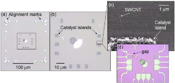
The substrate consist of 500 nm SiO2 on a highly doped silicon wafer (acceptors Sb, resistivity m cm), which is used to electrostatically change the potential of the SWCNT. First alignment marks are defined by electron beam lithography (EBL) as shown in Fig. 1a. The resist used is double layered consisting of 6% copolymer followed by 2% PMMA. Both layers are spun at 4000 rpm, 45 s and baked on a hotplate at 185 ∘C for 90 s. The EBL is done on a JEOL JSM-6320F scanning electron microscope (SEM) with Elphy software at 30 kV with a sensitivity of 200 C/cm2 and currents of pA and pA for small and big patterns, respectively. The pattern is developed in MIBK:IPA (1:3) for 60 s stopped by 30 s in IPA. The sample is ashed for 20-40 s in an oxygen plasma prior to deposition of 60-70 nm Cr. Lift-off is done in acetone.
The same EBL procedure is used to make the pattern for the catalyst islands. The catalyst liquid is spun on the sample at 4000 rpm for 150 s and baked at 185 ∘C for 3 min. to ensure that the catalyst sticks to the substrate. Lift-off is made in acetone and ultrasound if necessary. Figure 1b shows an optical image of the catalyst islands. The sample is now transferred to a chemical vapor deposition (CVD) tube furnace, where SWCNTs are grown in a controlled mixture of argon, hydrogen and methane (Ar: L/min, H2: L/min, CH4: 0.5 L/min). The optimal growth temperature depends on the thickness and the area of the catalyst islands. Typically, the temperature used is in the range of ∘C. After each growth the sample is examined in a SEM on a test area, which might appear similar to the picture shown in Fig. 1c. Sometimes several trials are needed changing the temperature to achieve an appropriate density of tubes. The test area ensures that the SWCNTs in the regions for devices are not exposed to the electron beam, which might damage the SWCNT. On the catalyst island and within a micron, the nanotubes grow rather densely. However, one or a few tubes ”escape” to distances of several microns. The contacts are aligned relative to the catalyst island and placed some microns away by EBL (no oxygen plasma step). Thus it is likely that only one SWCNT lies in the gap between the two electrodes. The Pd or Ti is evaporated by thermal evaporation, while Nb is DC-sputtered in an Ar atmosphere. Typical layers used are 4 nm Ti (or Pd) followed by 60 nm Nb and capped by 10 nm Ti (or Pd). Finally bonding pads of Au/Cr are defined by optical lithography.
3 Coulomb blockade regime
We first present measurements of a Pd/Nb/Pd contacted SWCNT with poor transparency that leads to Coulomb blockade at low temperatures.
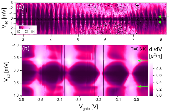
Figure 2a shows a bias spectroscopy plot of such a device where clear Coulomb blockade diamonds are seen with charging energies of mV. At low bias a dip in the differential conductance is observed due to the tunnel-like behavior of the device reflecting the density of states of the superconducting leads.[16] The green arrows point to the onset of quasiparticle tunneling V. In Fig. 2b a zoom of another slightly more conducting gate region of the device is shown. The onset of quasiparticle tunneling is clearly revealed (green arrows) and some conductance in the resonances is seen below the gap which is attributed to Andreev reflections. Such regular behavior has been observed in several devices with niobium based contacts and poor transparency. The onset of quasiparticle tunneling corresponds to a critical temperature of the K consistent with the features vanishing above . This critical temperature is much lower than the critical temperature measured in the niobium film and is properly due to poor proximity effect into the lower palladium layer in contact with the nanotube.
4 Supercurrent and the Kondo effect
The next device is more conducting and thus belong to a transparency regime where the Kondo effect can be observed, when the SWCNT quantum dot has a net spin.[15] The contacts are made of a Ti/Nb/Ti trilayer.
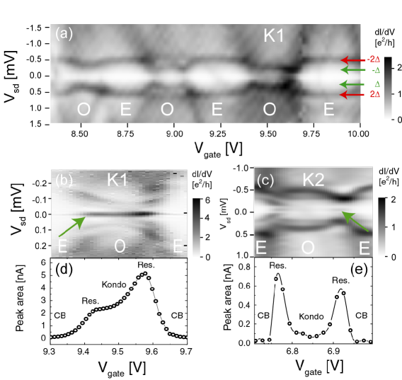
Figure 3a shows a bias spectroscopy plot in a gate region with an even-odd filling of single particle levels marked by the letters E/O. The Kondo resonances are identified by the clear change in magnitude of the features for the onset of quasiparticle tunneling () and one Andreev reflection (). For even electron filling, the onset of quasiparticle tunneling is more pronounced because quasiparticle tunneling is a lower order process than one Andreev reflection and transport happens via cotunneling in the Coulomb blockade region. However, when the Kondo effect is present (odd filling), a resonance exists at the Fermi energy of each contact leading to resonances for one Andreev reflection processes at . This qualitative explanation depends on the relative magnitude of and . We also note that this effect has been observed in other Kondo devices.[5, 17]
Figure 3b shows the Kondo resonance K1 at low bias voltages where the high conductive black region (green arrow) reflects a zero bias peak in dI/dV versus bias.[5, 4] We interpret this peak as a noise smear proximity induced supercurrent with an estimated magnitude given by the area of the peak (not the whole area under the peak). This interpretation is supported by the successful analysis of an analogous zero bias peak interpreted as a supercurrent in an open quantum dot.[4] We do not believe the peak to be a narrow Kondo resonance since it is present in the Coulomb blockade regions with even filling as well. Figure 3d shows the zero bias peak area versus gate voltage across the Kondo resonance. The peak is maximum in each Coulomb blockade resonance and also present in the Kondo resonance, while it is heavily suppressed in the Coulomb blockade regions.
Figures 3c and 3e show another Kondo resonance (K2) with a smaller zero bias peak. Similar behavior is seen in this Kondo resonance: Maxima of the zero bias peak area in the Coulomb blockade resonances and a small finite value in the Kondo resonance region, while the zero bias peak area is fully suppressed entering Coulomb blockade. These behaviors are qualitatively expected for a supercurrent and could be consistent with K2 having a lower Kondo temperature than K1. We are unfortunately not able to turn off the superconductivity in the leads in the setup used and more experimental work is needed to determine the relation between the zero bias peak area and .
5 Conclusion
We have succeeded in making weak links between niobium based leads, where the link is a high quality SWCNT. At low temperature the devices behave as quantum dots with observation of Coulomb blockade and Kondo effect. In the case of closed dots the onset of quasiparticle tunneling is clearly revealed. For more open dots a zero bias peak interpreted as a supercurrent is enhanced in Coulomb blockaded diamonds with an odd number of electron compared to diamonds with an even number due to the presence of a Kondo resonance.
Acknowledgments
We like to thank Jørn Bindslev Hansen and Inge Rasmussen for assistance and use of their niobium sputtering machine. This work is supported by the Danish Technical Research Council (The Nanomagnetism framework program), EU-STREP Ultra-1D program and the Nano-Science Center, University of Copenhagen, Denmark.
References
- [1] K. K. Likharev, Rev. Mod. Phys. 51, 101 (1979).
- [2] C. W. J. Beenakker, cond-mat 0406127 (2004).
- [3] P. Jarillo-Herrero, J. A. van Dam, and L. P. Kouwenhoven, Nature 439, 953 (2006).
- [4] H. I. Ingerslev, K. Grove-Rasmussen, T. Novotný et. al., cond-mat 0510200 (2005).
- [5] K. Grove-Rasmussen, H. I. Ingerslev, and P. E. Lindelof, cond-mat 0601371 (2006).
- [6] M. Bockrath, D. H. Cobden, P. L. McEuen et. al., Science, 275, 1922 (1997).
- [7] L. I. Glazman and K. A. Matveev, JETP 49, 659 (1989).
- [8] M.-S. Choi, M. Lee, K. Kang, and W. Belzig, Phys. Rev. B 70, 020502(R) (2004).
- [9] F. Siano and R. Egger, Phys. Rev. Lett. 93, 047002 (2004).
- [10] M. R. Buitelaar, T. Nussbaumer and C. Schönenberger, Phys. Rev. Lett. 89, 256801 (2002)
- [11] A. F. Morpurgo, J. Kong, C. M. Marcus, and H. Dai, Science, 286, 263 (1999)
- [12] J. Haruyama, A. Tokita, N. Kobayashi et. al., Appl. Phys. Lett. 84, 4714 (2004)
- [13] A. Yu. Kasumov, R. Deblock, M. Kociak, B. Reulet et. al., Science, 284, 1508 (1999)
- [14] M. R. Buitelaar, W. Belzig, T. Nussbaumer et. al., Phys. Rev. Lett. 91, 057005 (2003)
- [15] J. Nygård, David H. Cobden, P. E. Lindelof, Nature 408, 342 (2000)
- [16] V. Krstić, S. Roth, M. Burghard et. al., Phys. Rev. B 68, 205402 (2003)
- [17] T. S. Jespersen M. Aagesen, C. B. Sørensen P. E. Lindelof, and J. Nygård, to be published.