Level-occupation switching of the Quantum Dot, and phase anomalies in mesoscopic interferometry
Abstract
For a variety of quantum dots, the widths of different single-particle levels may naturally differ by orders of magnitude. In particular, the width of one strongly coupled level may be larger than the spacing between other, very narrow, levels. We found that in this case many consecutive Coulomb blockade peaks are due to occupation of the same broad level. Between the peaks the electron jumps from this level to one of the narrow levels and the transmission through the dot at the next resonance essentially repeats that at the previous one. This offers a natural explanation of the salient features of the behavior of the transmission phase in an interferometer with a QD. The theory of this effect will be reviewed with special emphasis on the role of the interactions. New results on the dot-charging measurements and the fine structure of occupation switchings will be presented, accompanied by the unified description of the whole series of CB peaks caused by a single broad level. We then discuss the case where the system approaches the Kondo regime.
pacs:
73.23.-b, 73.63.Kv, 73.23.Hk, 03.65.Vf1 Introduction
The challenging results of the experiment [1] which employed the double slit interference scheme in order to determine the phase [2] of the wave transmitted through a quantum dot (QD) in the Coulomb-blockade (CB) [3] regime is discussed in several articles of this volume. The unexpected result of this experiment was a repeated fast jump of the phase by between the resonances near the minimum of the transmitted current. [The phase at each CB peak increased smoothly by in accordance with the Breit-Wigner picture.] In this paper we will first review the mechanism intended to explain these experimental findings suggested in our paper Ref. [6] and then discuss new features and results. The essence of our suggestion in Ref. [6] was the observation that if a QD happens to support a single level extremely well coupled to the leads, the conductance for a series of charging resonances will be governed by the transport through (population of) this level. Other, narrow, levels are occupied, and the broad level is repeatedly depopulated via (almost) abrupt occupation jumps in the CB valley. This interlevel electron-exchanging mechanism, which has later been dubbed ”population switching” (although the notion ”level-occupation switching” may better reflect the physical situation), can lead to a satisfactory explanation of the experiment. The first suggestion of occupation switching as a possible explanation for the phase lapses and peak correlations (see below) was given in Ref. [7] and followed up in Ref. [8]. However, that mechanism was due to an assumed special structure of the dot, not to electron correlations as in the present work.
Another important result of the experiment [1], which also disagrees with a number of models, is the similar shape and height of consecutive CB peaks. This effect, which is often not emphasized enough, is again naturally explained within our picture.
Experiments of the Weizmann group [1, 4, 9, 10, 11] measuring the transmission phase in QD-s have stimulated a wide theoretical interest, which is (partly) reflected by Refs. [7, 8, 5, 12, 13, 14, 15, 16, 17, 18, 19, 20, 21, 22, 23, 24, 25, 26, 27, 28, 29, 30, 31]. In particular, the phase behavior observed in Ref. [1]: an increase by at the resonance accompanied by a sharp jump in the CB valley, is in evident contradiction with what one would expect had the transmission of the current proceeded via consecutive levels in a 1-dimensional quantum well. In a two–dimensional QD the phase drops associated with the nodes of the transmission amplitude arise already within the single–particle picture [14, 15, 16], related to the Fano effect. However, in order to have a sequence of such events one should consider a QD of a very special shape or level structure, which is not expected in the generic case [13]. The model of Ref. [19] also does not allow to explain the series of drops, especially at very low temperatures. The mechanism of Refs. [7, 8], as we already mentioned, makes nontrivial assumptions on the geometry of the QD and the way it changes under the change of plunger gate voltage. A generic mechanism suggested in Ref. [20] may indeed lead to the correlations in transmission at many consecutive valleys, but the predicted phase behavior differs from what has been seen experimentally.
The mechanism for charging of the QD, which we will discuss in detail in the next section includes two important ingredients. One is the necessity of the existence of levels anomalously coupled to the leads in sufficiently large irregular QD-s. The mechanism suggested for this purpose in our paper Ref. [6] will be reviewed in Sec. 2.2. Further developments of this and related mechanisms may be found in Refs. [13, 29, 32]. In all these cases the broadening of the single particle level does not require the electron interaction in the QD.
The second ingredient is the interaction-induced occupation switching, which we describe in section 2.1. Further developments or applications of this effect, also discussing applications not related to the transmission phase problem, may be found in Refs. [23, 33, 24, 36, 25, 34, 35]. Finally, recent papers [17, 18] investigated, invoking the Fano effect and the dynamically generated level broadening [32], both the universal regime, where phase lapses generically occur, and the mesoscopic regime, where the phase behavior is irregular, as in Ref. [11]. The crossover between these two regimes as a function of a single parameter, was also discussed.
Our main effort in the first parts of this paper will be to explain clearly the basic physics of the effect of level-occupation switching in the simplest cases, precisely defining the effect of the interaction. Effects of the electron spin [21] will be discussed in Sec. 3, while new results on the details of occupation switching will be treated in Sec. 4. The case where the QD approaches the Kondo regime [22] will be considered in Sec. 5 in relation with the experiment of Ref. [9]. We conclude with some remarks on where the theory stands vis a vis the explanation of the experiments.
2 A model for the level-occupation switching
A useful theoretical model for the description of charging effects in QD-s is the tunneling Hamiltonian in the constant interaction () approximation (see e.g. [3])
Here and are the annihilation(creation) operators for electrons in the dot and in the lead and are the single-particle energies. We do not introduce the dependence of the tunneling matrix elements . Summation over spin orientations is also easily included, but we first treat the spinless case (which is experimentally realizable by applying a strong enough magnetic field to the dot. To avoid the orbital effects of the field, it may be applied parallel to the plane of the dot). Under the assumption of capacitive coupling to the gate, the levels in the dot flow uniformly with the voltage
| (2) |
The energy of an electron in the wire with momentum is given by
| (3) |
Although the experiment [1] was clearly done in the CB regime, the widths of the resonances turned out to have been anomalously large, only few times smaller than the charging energy and larger than the dot’s level spacing. Also, the widths and heights of all observed resonances are very similar. These surprising features of the results of Ref. [1], which have not attracted so wide an attention as the phase jumps, motivate us to consider the model in which the QD supports a single very broad (well coupled to the leads) level, which we describe in the next subsection. Widths of all other levels will be assumed to be small and may be set to zero in the leading approximation.
It is generally believed that the CB is observed only if the widths of resonances are small compared to the single-particle level spacing in the dot [37]. This condition assumes that the couplings of all levels to the leads are of the same order of magnitude. However, as we will show below in section 2.2, for many situations the widths of the resonances may vary by orders of magnitude. In this case it does not make sense to compare the width of few broad resonances with the level spacing, determined by the majority of narrow, practically decoupled, levels. [Even the case of a single level being wider than the charging energy may be considered within our approach [33].]
2.1 The case of a single broad level
Now we turn to the many-particle effects arising for the Hamiltonian (2) in the case of only one (-th) level in the dot coupled strongly to the wires, , . If the width of this level is larger than the single-particle level spacing , a very nontrivial regime of charging of the QD may be described by means of second-order perturbation theory estimates (compare with Ref. [38]). This simple treatment produces all the important features of the problem (a similar approach was used recently in Ref. [39] for the calculation of CB peaks positions).
The width of the well coupled level is given by
| (4) |
The widths of the other levels are taken to be much smaller than the level spacing and may be neglected in the first approximation. The charging energy is still very large . We shall show that transmission of a current at about consecutive CB peaks will proceed through one and the same level . Let the levels with in the QD be occupied. Our aim is to find the total energy of the true ground state of the dot at different values of . Without loss of generality we may assume that the summation over in Eq. (2) goes only over . (Thus we subtract from the total energy the trivial constant corresponding to selfinteraction of electrons with . Coulomb interaction between electrons at the levels with and is included into .) We also subtract from the total energy the trivial energy of electron gas in the leads .

In this section we consider spinless electrons. We use a superscript in the total energy of the many-electron ground state to denote the number of electrons, , in the narrow levels (with ) in the QD. Thus and stand for zero and one electron in the narrow levels, respectively. We start with and with the case of large positive . The only nontrivial contribution to the total energy is given by the second order correction where an electron hops from the lead to the level and back,
| (5) |
To calculate the integral here we use that , where is the length of the wire and the energy and momentum are related by Eq. (3). In Eq. (5) and everywhere below, are functions of (2). When with the increasing voltage the decreasing energy level crosses the region the level becomes occupied (occupation of the level is energetically unfavorable, as we will see below, even though ).
The total energy of the system (with all the subtractions described above) may be calculated similarly to Eq. (5) for (the broad level being well below the Fermi energy). The two contributions to are now the energy of the electron in the dot (which was taken where from the state in the lead (3)) and the second order correction describing the electron hopping from the level to the leads. This gives
| (6) |
Alternatively, Eqs. (5) and (6) may be derived without explicit reference to many-body perturbation theory. To this end we first perform a unitary rotation of the lead states such that only a single effective lead defined by the annihilation operator remains coupled to the dot. In the absence of the QD level the levels in this lead are quantized via . Adding a discrete QD level to this dense grid of the lead levels results in a slight shift of the new levels with respect to the old ones (see e.g. the book [40]). The levels with are shifted downwards, while the ones with are shifted upwards. The individual shift of any level is smaller than the level spacing in the lead (), but the accumulated effect of the shifts of many () levels lead to a visible correction to the total energy. The sum of the downward shifts of all (full) levels with in case of () gives Eq. (5). The second term in Eq. (6) (the case of ) contains two contributions: a negative one due to the shifts of levels with , and a positive due to the shifts of the levels with . A perturbative calculation of this correction becomes possible because of the cancellation of contributions from regions and .
Finally, a precise treatment for a single state interacting with a continuum for spinless electrons yields [6]:
| (7) |
which coincides with the Eqs. (5,6) at and gives the correct interpolation between them.
Let us now consider the branch where the level is occupied (which we label by the superscript ). The energy of the electron in the QD is . However, the energy of the empty level is now increased by , due to the interaction. Adding one more electron via the hopping from the Fermi level in the lead, to that level, now costs . The ensuing reduction of the downward shift of the level is of crucial importance. This is precisely where the effect of the interaction is felt. The analog of Eq. (5) for now reads
| (8) |
Without the interaction , the two second-order correction terms on the RHS’s of Eqs. (6) and (8) are equal. This explains why these corrections to the total energy of the system do not affect the order of level populations in the noninteracting QD. For the case considered, , level will be the first to be filled when its energy crosses the Fermi level in the leads, , as is shown by a thick dashed line in Fig. 1.
With the interaction , after the electron is added to the dot the second order corrections in Eqs. (6) and (8) start to depend on which of the orbitals or is occupied by this electron. In a large part of the CB valley the energy gain because of the increased second order correction overcomes the loss, , caused by the raising the electron from the level to the level . The true ground state of the system here will be (6). The two functions and cross at
| (9) |
and the ground state jumps onto the branch . Here the ”active” electron inside the dot is transferred from the broad level to the narrow one . The energy of the current-transmitting virtual state becomes positive again, . Thus, the phase of the transmission amplitude has returned to what it was before the process of filling of level and the subsequent sharp jump into the state where level is filled. It is the latter jump which provides the sharp drop by of the transmission phase, following its gradual increase by through the broad resonance. Fig. 1 illustrates the behaviors of the bare levels and the renormalized ones, including the crossing of the latter at the switching point.
For the case considered so far, where the width of the narrow level vanishes, the switching transition is infinitely sharp. However when the coupling of level is switched on, second-order processes involving jumps from level to the lead and back from the lead to level (or vice versa) will create a matrix element connecting these two states. This makes the crossing of the energies and , considered above, an ”avoided” one, and provides a finite width for the switching transition.
Even when the switching transition is broadened, the phase jump should still be abrupt (has zero width) in case of spinless electrons, as was proven in Ref. [21]. Fast phase drops in the valley are associated with nodes of the amplitude, , where is close to the real axis (small ). For spinless electrons, the linear conductance (even through the interacting QD, since we are interested in the elastic processes) is determined by a single complex amplitude, , which is the amplitude of transmitted electron wave in e.g. the right lead for unit amplitude of the incoming wave, , in the left lead. [In case of spin the linear conductance would be given by a sum of the squared moduli of several complex amplitudes describing the scattering for different orientations of the electron spin and the spin of the QD, including spin-flip amplitudes, while the Aharonov-Bohm phase will be determined by the phase of the sum of non-spin-flip amplitudes, as discussed in Sec. 5 below]. The vanishing of the transmitted electron wave at means the existence of a solution of the Schrödinger equation with in one lead. If the Hamiltonian is time-reversal symmetric, the complex conjugated wave function should also be a solution with the same boundary condition and , hence . The phase changes abruptly by when the real energy crosses the Fermi energy. [For the phase jumps associated with the exact vanishing of the conductance there is no way to distinguish between and jumps. This ambiguity is resolved, after the phase jump acquires a some width [22, 26], due to e.g. a finite temperature.]


For the occupation switch taking place not too close to the charging resonances, detailed calculations of the conductance and phase behavior, may be done within the so called ”elastic cotunnelling” approximation, as we shall describe in Sec. 4.2. Resulting from the destructive interference of quantum amplitudes, the exact vanishing of the transmission amplitude here has some similarity to the celebrated Fano zero. The broadening of the phase lapses in the case of broken time reversal symmetry was investigated in Ref. [24].
The level-occupation switching guarantees the universal occurrence of the phase jump. Otherwise, it depends on the relative signs of the matrix elements connecting the states of the dot to the leads [26, 27, 28]. For example, the zeroes of the amplitude do not occur in the one dimensional case, but should be found in about a half of the spin zero valleys in a two-dimensional QD. While interesting effects can be found by adjusting these signs, we believe that a more universal mechanism is called for.
When there are a number of narrow levels in the vicinity of the broad level, the above process can repeat many times. From Eq. (9), we see that the number of narrow levels which switch occupations with the broad one is on the order of (). Thus the above number of consecutive resonances are due to the transition via one and the same level . Obviously, the conductance and the phase shift (including the jumps) will be very similar for all these resonances, as long as they occur near the middle of the CB valley. When the occupation switch occurs close enough to a CB peak, the shape of that peak will also be deformed (see below). For other peaks, the phase will increase in a Breit-Wigner way by around each resonance and sharply jump down by at the switching point between the resonances. There is really no need for ”further calculation” of this phase behavior.
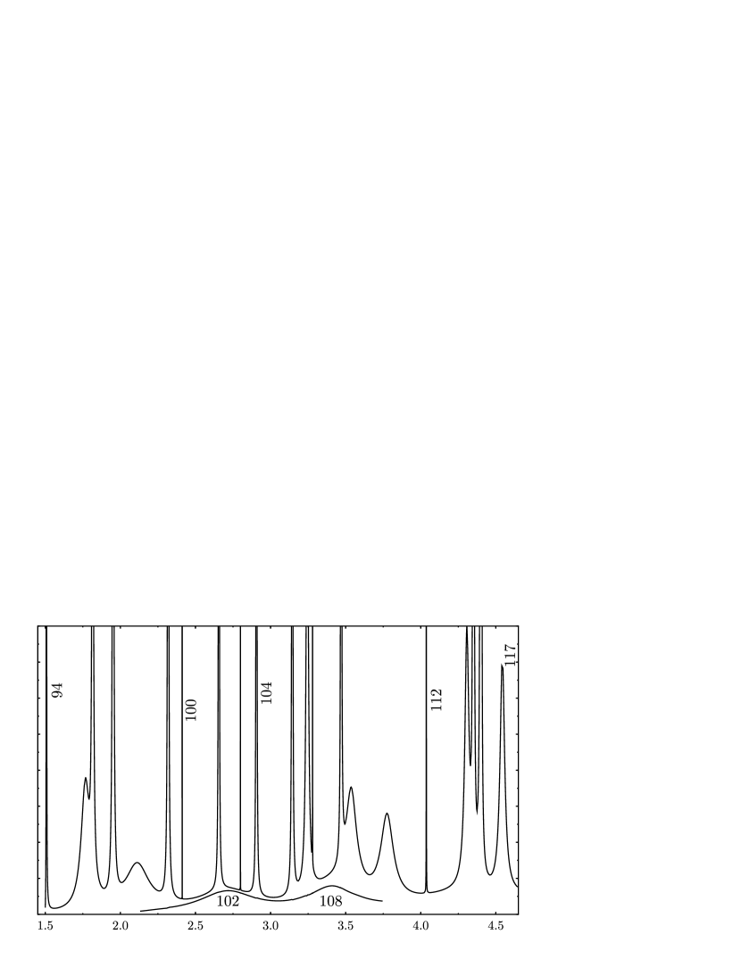
An example of such a series of consecutive resonances is shown in Fig. 2. We note the typical increasing asymmetry of the conductance peaks while going away from the center of the CB valley. A peak asymmetry with a qualitatively similar structure has in fact been observed by Lindemann et. al. [41]. It was interpreted as due to the conductance being determined by a special ”bouncing ball” state having a width much larger than the others [29]. The mechanism invoked appears however to be different from the one described here.
For the tails of series of peaks shown in Fig. 2, the occupation switch takes place within the charging resonance. With increasing relative peak number, , the usual narrow Breit-Wigner peaks in the conductance due to a population of level should be formed here. The shapes of these peaks, as well as (possible) Fano-type conductance zeroes and -phase drops will be strongly affected by the many-body orthogonality catastrophe and their investigation goes far beyond the scope of this paper.
For electrons with spin, the Breit-Wigner-related formula (7) does not work, but the perturbative formulas such as (5) and (6) may be still used away from the resonances. We will discuss the new effects caused by spin in section 3. Before that we explain in the next subsection why our model is likely to apply for a generic (smooth) QD with mixed classical dynamics.

2.2 Justification of the model
We now discuss the conditions for obtaining levels with strongly varying widths in the QD.
An example of a system for which the widths differ drastically is the integrable QD [7, 8]. However, it is hard to believe that the large () QD may be even close to integrable. Nevertheless, at least in classical mechanics, a considerable gap is left between integrable and fully chaotic systems. Even in a nonintegrable dot two kinds of trajectories - quasi-periodic and chaotic - may coexist. In this case, in 2-dimensions any trajectory (even a chaotic one!) does not cover all the phase space allowed by energy conservation. Consequently, the corresponding wave functions do not cover all the area of the QD. If such a regime is realized in QD-s, it easily explains why the widths of the resonances may vary by orders of magnitude. Moreover, many other features of such a QD may differ strongly from those of the chaotic QD [42]. An explicit numerical example, which supports the existence of such a regime is given below [6]. We require the QD not to be fully chaotic (neither do we require an integrable QD). It is not clear, how chaotic was the dot used in the experiment. However, the QD containing electrons was times smaller than the nominal elastic mean free path. Thus, disorder should not have been essential for the dynamics of the electrons.
To illustrate the relevance of the model Eq. (2) with single strongly coupled level we performed numerical simulations for a model QD of a size with a simple polynomial potential (a smooth QD coupled to two leads)
| (10) |
Due to the strong mixing of the and coordinates the dot is expected to be nonintegrable, but, similarly to the experimental geometry [1], it is approximately symmetric. For simulations we considered the QD on the lattice and used which was equivalent to lattice spacings. The kinetic term is given by the standard nearest neighbor hopping. Below we present the results of calculations with the hopping matrix element which corresponds to the dot with electrons or if the spin is included (similar numbers to those in the experiment). We have used the potential of Eq.(10) for . The lead formed by the potential was attached at and a hard wall was put at . Within the energy interval exactly one mode may propagate along the lead. The analysis of solutions of the Schrödinger equation within this interval allowed us to find the positions and widths of quasi-stationary levels in the dot. As we expected, the widths fluctuate very strongly from level to level (by many orders of magnitude). In particular the widths of two levels and exceed sufficiently the level spacing (the number of states doubled due to spin). The origin of the hierarchy of widths becomes clear from fig. 1, where we have plotted in the QD for (real) at the top of corresponding resonances. The quantized version of different variants of the classical motion may be found in this figure. The narrowest level corresponds to a short stable transverse periodic orbit. Other broader levels, such as , may be considered as the projections of the invariant tori corresponding to quasi–periodic classical motion. This classical trajectory reaches the line only at few points. The candidates for chaotic classical motion (e.g. ) also correspond to relatively broad resonances. Even in this case only a part of the QD is covered by the trajectory. For the most coupled levels and the area covered by the trajectory touches the lead by its corner.
Moreover, two well-coupled trajectories contribute to the level . This is seen from the fig. 2 where we show also the at the left and right wings of this resonance. One contribution corresponds to the strongly coupled quasi-periodic trajectory (left), having the “turning point” just at the left contact. The other contribution comes from the true periodic trajectory (right). Two quantum states in the dot become mixed via interaction with the wire and form one broad () and one almost decoupled () resonance [43]. [This mechanism was also found and investigated in ref. [32] and the relationship to the Dicke effect [44] highlighted. It will be further discussed at the end of this subsection.] We have repeated the calculations several times for slightly different and in a broad range of variation of the hopping. Typically, we saw resonances of very different widths and the origin of the broadest peaks was explained by simple classical arguments. The explicit example also allows to clarify the range of validity of our method. In addition to the evident conditions , we should also have , being the total number of electrons in the QD. For even the few broad levels start to overlap and the CB is expected to be eliminated.

Taking into account the different sensitivities of longitudinal and transverse modes to the plunger [7, 8] may allow to keep our broad level even longer within the relevant strip of energy. This may provide an explanation for the even longer sequences of resonances accompanied by the jumps.
In a more refined approach, adding new electrons into the QD should cause a change of the self-consistent potential . The total energy of the dot and the wire will be lowered in the presence of strongly coupled levels. This may cause the potential of the QD to automatically adjust to allow such levels, which will support our explanation of the experiment of Ref. [1].
The Dicke-type mechanism for the dynamic generation of anomalously broad levels was used for many years in nuclear physics [43]. In QDs the attention to this mechanism was recently attracted by Ref. [32]. The latter work also generalized the treatment to several channels. When several levels are coupled to a continuum and their widths are larger than their spacings, the couplings among them mediated by the continuum become important (the same coupling was alluded to as causing the avoided crossing of levels and in section 2.1). One now has to diagonalize the (nonhermitean, due to the finite lifetime of the levels) effective Hamiltonian matrix. In the simplest case, when all initial levels are degenerate, one of the resulting levels (the ”superradiant” one [44]) will acquire an width, while the remaining levels will become very narrow. This will still hold qualitatively when the level spacings do not vanish, but are smaller than the widths. Such a generation of one broad level was also found in a more general treatment, including the interactions and employing renormalization group (RG) approaches, in Refs. [17, 18].
We notice however, that our numerical example [6], described above, showed that it may not be easy to employ the Dicke mechanism in its full strength in a QD described by a realistic 2-dimensional potential. We were able to observe a formation of the superradiant state from two close resonances (levels and in Figs. 3 and 5). However, to arrange the situation with several overlapping resonances, necessary for this mechanism, is difficult since the averaged level width in realistic QD appears to be always smaller than the level spacing.
3 Effects of the electron spin
The goal of this section is to consider the new features which appear if one goes beyond the simplest model of the occupation switching considered in Sec. 2. This section will be concerned with the effect of the electron spin. Since adding the spin leads to a significantly more complicated picture, we consider in subsections 3.1 and 3.2 the case of a QD with only two levels, one well coupled and one negligibly narrow. [These two subsections present the results found in Ref. [21].] The experimental tendency towards producing small few-electron QD-s also encourages one to investigate systems with small number of levels. The case of many levels with spin will be discussed in Sec. 3.3.
3.1 Two levels with spin, level-occupations and the ground state energy
Charging effects with ”spinful” electrons are described by the same tunnelling Hamiltonian Eq. (2), where now all summations include the summation over the spin index as well. We consider a QD with two levels, whose energies depends on a gate voltage and level splitting as in Eq. (2)
| (11) |
Only one level, , is well coupled to the leads, having the width (4)
| (12) |
The dot is charged by one electron at and .
Our first aim will be to find the ground state of the system (11,12) at different values of in the limit . Similarly to Sec. 2, let us denote by the total energy of the lowest state of the QD interacting with the leads, with the narrow level populated by, respectively, and electrons (more precisely, is defined as the eigenenergy of the Hamiltonian (2) minus the trivial energy of the electrons in the leads ). The functions evolve smoothly with the gate voltage and the (averaged) occupation number of the broad level also changes continuously. For example, the branch corresponds to an empty level at , singly occupied at and doubly occupied at . For the functions cross at some values of , which lead to sharp changes of the ground state.
With the use of perturbation theory in it is easy to find far from the charging peaks. Below the first resonance (at ) the true ground state is evidently . However, already here the virtual jumps of the electrons from the wire to the level give rise to the correction
| (13) | |||
The extra factor in compared to Eq. (5) accounts for the spin. It is clear that in this region lies significantly below and . When the (increasing) voltage crosses the region , the dot is charged by the first electron. However, this electron may stay in the dot on the level (described by ) or on the level (). Depending on what level is occupied the perturbation theory gives, in this range of
| (14) | |||
The first logarithm in accounts for the virtual jumps of an electron from the level in the dot to the wire. The other logarithms correspond to virtually adding the second electron to the dot (having or instead of in the denominator). The two levels and cross at a gate voltage (compare to Eq. (9))
| (15) |
This result is valid for both signs of . For , Eq. (15) reduces to . At the electron in the dot jumps from the broad level to the narrow one.
In the second valley, the dot is charged already by two electrons, which again may populate the two doubly degenerate levels in the dot in different ways. Here one finds,
| (16) | |||||
First of all, we see that just after the charging peak, at , the true ground state is . This is in contrast with the situation at , where the ground state was (14). Thus we may conclude, that within the resonance not only is one electron gradually transmitted from the wire to the level in the dot, but also a second electron is taken from the narrow level to the broad one (see fig. 6). In the limit this second “transfer” is abrupt and takes place at some (for zero temperature, ). This prediction of the possibility to have sharp features within the charging resonance is the main new effect caused by the spin. All the three energies (16) cross at the same value of gate voltage (c.f. (15))
| (17) |
and the true ground state becomes . Now already two electrons jump together from the broad level to the narrow one. At (15) the occupation of the quantum dot proceeds in a fashion symmetric to the above. At the third peak the third electron is added to the dot. Were the branch the stable one, this would have been the uncoupled electron at the level . However, and cross at the top of the third peak (at ) and the ground state for the first half of last valley has a single unpaired electron at the narrow level. Finally, at
| (18) |
and cross and the broad level becomes singly occupied again. The fourth peak () completes the charging of two levels in the quantum dot by four electrons.

To summarize the discussion of this subsection, we show schematically in Fig. 6 the averaged occupation numbers of our two levels and . The four charging resonances correspond to . One may see on the figure many abrupt changes in the occupation of both broad and narrow levels. The occupation number of a given level is not measured directly in the experiment. However, the appearance of an occupation switching may be seen in the signal of a suitable QPC detector [45] as we describe in Sec. 4.1. In the following subsections we discuss the transport properties of the QD with a single broad level for ”spinful” electrons.
3.2 Two levels with spin. Conductance
The zero bias conductance of our two-level quantum dot is shown schematically in Fig. 7. In the limit of an ”invisible” level (), we may introduce three conductances corresponding to empty, singly-occupied and doubly-occupied narrow level (characterizing the three ”ground state” energies of the previous section). The role of the electrons in the level reduces in this case to simply raising the current-transmitting level via the Coulomb repulsion. Thus
| (19) |
We have shown schematically the function on the same Fig. 7 (vertically offset). In the limit the curve for a two-level dot is obtained simply by cutting and horizontally shifting the parts of the curve for the single-level dot, in agreement with Eq. (19), as shown in the figure. Thus the relations Eq. (19) allow one to describe the singular behavior of the conductance even without an explicit calculation of .

The sharp features seen in Fig. 7 will be smeared at finite temperature (see examples in Ref. [21]). To resolve them one needs to measure the conductance at . If the temperature is still large compared to the Kondo temperature, , the conductance away from the resonances may be found by calculating the transmission tunneling amplitude in the second order of perturbation theory (”elastic cotunnelling”). This gives,
| (20) | |||
The first line in Eq. (20) is for an empty dot. The second line describes the current through the QD having one electron on the level . The current in this case is a sum of three contributions [21] accounting respectively for the spin-flip processes, transmission of the electron with the spin parallel to the spin of the electron in the QD and transmission of the electron with antiparallel spin. Note that the spin-flip contribution vanishes at , as it should. The last line in Eq. (20) is for the case of two electrons on the level .
Two kinds of sharp features are seen in Fig. 7. First, both a cusp and a jump take place at the peaks: , where the curve is replaced by and , where is replaced by . The jump vanishes for , but the pronounced cusp survives even for . Currently, no theory exists which would describe the fate of these singularities at and finite (small) coupling to the leads of the level .
Besides the above, there are three jumps of in the valleys. The values of the conductance at the borders of the first jump, at are (assuming )
| (21) |
The contribution from the spin flip processes for is twice that from the elastic processes. Therefore, the conductance drops near by a factor of 3. At the two electrons jump from the broad to narrow level. The discontinuity at , which follows from the small difference in the probability of the electron-like and hole-like processes, vanishes for (restoration of particle-hole symmetry at ). Examples which find the fine structure of such jumps at will be given below.
3.3 Many levels with spin

A straightforward generalization of the theory presented in previous two subsections allows one to find the conductance (and level occupancies) for a multilevel QD with a single broad level, , for ”spinful” electrons. The resulting conductance behavior is shown in Fig. 8 (compare with Fig. 2). Similarly to the case of 2-level dot, considered in Sec. 3.2, the conductance curve may be found by cutting and gluing the parts of the curve describing a QD with single (spinful) level. In contract to Fig. 7 we now consider the case of zero temperature (). Thus the ”generating function” for conductance of multilevel QD is now the conductance at for the Anderson impurity model [46], shown by thin dashed line in the figure. [An exact Bethe ansatz solution for this model [47] gives explicitly.]
The series of peaks shown in Fig. 8 contains three large, , sets with qualitatively different charging scenarios. First comes a sequence of peaks ( in the figure) having one occupation switch per charging event. At the left wing of each resonance here the broad level in the QD is empty and is gradually populated with the increasing . Somewhere inside the charging resonance it becomes energetically favorable to populate one of the narrow levels in the dot by single electron. The broad level is depopulated at this moment and its energy is raised, . A reliable description of the fine structure of such an occupation switching for a finite coupling of the narrow levels to the leads, remains a challenging theoretical problem (similarly to the case of spinless electrons of Sec. 2.1).
With further increase of the gate voltage the occupation switching, for a series of peaks, splits into two parts. Now inside each peak one electron jumps from the narrow to the broad level in the dot. Such events for 2-level case were considered in previous subsections ( and ). Thus within a single charging resonance the well-coupled level in the dot becomes occupied by two electrons. Between the resonances both electrons from the broad level jump to narrow ones. This is where one will see the jumps of the transmission phase in the CB valley.
Finally, for a series of peaks the charging events start (left wing of the resonance) in the situation when the broad level stays inside the QD () being populated by two electrons. Then, at a certain voltage, an electron from a lead jumps onto the QD narrow level. Repulsion from this electron raises the broad level, , and partially depopulates it. The occupation of the level is completed again at the right wing of the resonance.
The important consequence of the scenario presented in this section is the absence of the Kondo effect for a large series of charging resonances, which might be easy to verify experimentally.
4 Sharp features and charge detection
In subsections 4.1 and 4.2 we considered the effects which appear if one takes into account the finite width of the narrow level. Since the particular features considered here do not depend on the spin the discussion is narrowed to spinless electrons only.
4.1 Sharp features: QPC detector signal
In this subsection we investigate the fate of the sharp features in the CB valley considered before, if the narrow levels in the QD acquire a small but finite widths. Let, as in Sec. 3.1, 1 be a broad level and 2 be a narrow one in the QD. First, in a way analogous to Eqs. (4,12) we introduce the width of the second level and the interlevel coupling . Consider a CB valley where there is one electron in the dot either on the level 1, or on the level 2. The dynamics of QD is described by the effective single-particle Hamiltonian, accounting for the coupling to the leads, whose matrix elements are () [21]
| (22) |
Here and are nothing more than the renormalized single particle energies and , similar to Eqs. (6,8) minus a proper constant. In the argument of the logarithm may either be or , since . For simplicity we consider the time reversal symmetric case, . Eq. (4.1) is valid for an arbitrary ratio of couplings of two levels to the leads. In the general case however, the width of the level switch may become of order (see Eq. (28) and remark below it). Below we consider the sharp switch case, , .

For electrons with spin there are two species of the effective Hamiltonian Eq. (4.1) for each spin orientation. [If in addition the QD has one electron for each spin, there are no spin-flip transitions in the linear conductance.] In this and in the next section we consider spinless electrons.
Examples of resolving the sharp features in the conductance based on the avoided level crossing described by Eq. (4.1) may be found in Ref. [21]. Here we give only two examples, which seemingly have not been covered in the existing literature.
Using a side quantum point contact (QPC) as a charge detector [45] becomes now an efficient experimental tool for finding the number of electrons in small QDs, complimentary to the transport measurements. The same device may obviously be used to detect the occupation switching [36].
The ground state of the system described by the Hamiltonian (4.1) is a superposition of two states
| (23) |
For weak coupling between the QD and QPC the transmission amplitude through the latter reads ()
| (24) |
where is some single-particle operator and both the background transmission amplitude and the matrix elements of weakly depend on the gate voltage . Thus we find the change in the QPC conductance
| (25) |
where and . To see explicitly the gate voltage dependence of we consider the case of a single broad level, . Now we may omit in Eq. (4.1) and use an expansion around the center of the switch ()
| (26) |
which allows us to write
| (27) |
Now, instead of Eq. (25) one has
| (28) |
The width of the occupation switch, , is always a fraction of the charging energy, becoming for . The function is shown in Fig. 9. Note the asymmetry of the step in the QPC signal and the maximum on one side of the step for .
4.2 Sharp features: Phase drops
While we declared in Sec. 2.1 that the phase lapses in the CB valley for spinless electrons should be abrupt and equal , the actual phase drops in Fig. 2 are always somewhat smaller than . In this section we show how this exact is restored after the coupling of the narrow levels is switched on (still we assume ). We also continue working with spinless electrons here.


To find the conductance and phase behavior we first notice that after having successfully employed the coupling of the narrow level to smoothen the occupation switch, there is no need to consider the contribution to the conductance from this small coupling. What we have now is a QD with two levels and (23), each coupled to the leads via tunneling matrix elements and . One level, , is occupied by the electron (energy ), the other level is raised due to electron repulsion ().
In the valley between two CB peaks, the conduction is dominated by the so-called elastic cotunneling (i.e.second order) processes through the resonances at larger and smaller energies. For example, tunneling first from the left lead to the dot (whose relevant state must then be empty beforehand) then from the dot to the right lead. This ”electron process” is dominant near the right-hand CB peak. The other possibility, dominant near the left-hand CB peak, where the relevant dot level is full, involves first a transition of the electron from the dot to the right lead, then from the left lead to the dot. Therefore, the latter process is termed a ”hole process”. For fermions, the hole process is well-known to acquire an extra minus sign. In our case, where due to the level-occupation switching, the two CB peaks are due to the same level, the transmission amplitude must have opposite signs in the two sides of the Coulomb valley. Thus the transmission amplitude in the time-reversal symmetric case must have a zero somewhere in-between. A simple calculation with the use of Eq. (23) now gives (we assume ).
| (29) |
To extract the transmission phase from this result we further notice that since the couplings of two levels to the leads are proportional we may perform a standard unitary rotation of the leads [48], , , to define one coupled () and one decoupled () lead. All transport properties are found from the -matrix for the single coupled lead, . In particular the transmission amplitude and conductance are (again )
| (30) |
This allows us to relate the conductance (29) and the phase of the transmitted wave . Fig. 10 shows the conductance and the phase behavior found from Eqs. (29) and (30).
5 The sensitivity of the transmission phase to Kondo correlations
Among the observations [49, 50, 51, 52, 53] of the Kondo effect [54] in quantum dots(QD) [48, 55, 56], two experiments [9, 10] were devoted to the measurement of the phase shift of the transmitted electron. These experiments were aimed at a direct observation of the fundamental prediction [57, 58] of the Kondo model: the phase shift experienced by the scattered electron after the spin of the impurity is screened into a singlet.
In agreement with the general predictions and the numerical renormalization group calculations [30] for an Anderson impurity [46] in Aharonov-Bohm(AB) interferometer, the development of a plateau of in the Kondo valley was seen in Ref. [9] (although the reported saturation value of the phase was not ). A very important, unexpected feature of the experimental results was the strong sensitivity of the phase to Kondo correlations: the phase saturated at , while the conductance in the valley was still well below the unitary limit, indicating the absence of Kondo screening.
Our aim in this section will be to explain this strong Kondo effect in the phase [6]. We will see that although the nontrivial phase behavior is indeed governed by the Kondo physics, the main changes of phase take place at temperatures parametrically larger than . In a sense, we show that the phase changes in the regime where, although the spin of the impurity is not screened, the running Kondo coupling constant exceeds parametrically its bare value.
The transmission phase is measured, as before, by embedding the quantum dot into one arm of the two-wave AB interferometer [1]. Let be the transmission amplitude for an electron with spin projection through the QD having a spin projection . Respectively, let be the transmission amplitude through the second reference arm. (Obviously, the spin- flip processes occurring in the QD and not in the reference arm do not contribute to the interference.) Now, the part of the current oscillating with the change of the magnetic flux threading the interferometer takes the form
| (31) |
We use the fact that (for the weak magnetic field used in the experiment) the transmission through the reference arm does not depend on spin. By measuring the relative phase of the AB oscillations at different values of the gate voltage one extracts the information about the transmission phase. We see that in fact in the interference experiment not a single amplitude is measured, but the sum of all possible amplitudes corresponding to different orientations of the spins of both the transmitted electron and the QD [19].
5.1 The single-level Anderson model.
Far from the charging resonances the interaction of the lead electrons with the dot is described by the Kondo Hamiltonian
| (32) |
Here and denote left(L) and right(R) leads, the operator annihilates the electron in lead with momentum and spin . The Pauli operators and the density of the conduction-electrons on the impurity are given by
| (33) |
Explicit formulas for and will be found below from the tunnelling Hamiltonian describing the QD. We will consider a time-reversal symmetric system. Then the matrices are real and symmetric.
The interaction of the conduction electron with the spin of the dot may be diagonalized by an orthogonal transformation [59] of into new operators and , described by the angle , . This gives
| (34) |
As long as the two couplings are renormalized independently
| (35) |
Here is the density of states in the leads. In the case of antiferromagnetic coupling ( ) this formula may be written in the form with being the Kondo temperature. Crucial for the understanding of the phase behavior is that in the leading order only the spin-dependent part of the Hamiltonian (32) is renormalized, while the scalar coupling remains unchanged, .
In the simplest case of only one level in the dot (Anderson impurity model), only one mode is coupled to the dot via the tunnelling matrix element , while the second mode remains completely decoupled. The bare values of the coupling constants in the Kondo Hamiltonian (32) are now given by the second order of perturbation theory
| (36) |
Here is the energy of the impurity level and is the charging energy and the Fermi energy is .
The non-spin-flip transmission amplitudes for parallel and antiparallel spins of the dot and the electron are
| (37) | |||
where . The imaginary part of the amplitudes here is formally of the fourth order in the tunnelling amplitudes . However, the calculation of the phase of transmission amplitude requires only the -matrix for non-spin-flip scattering to second order in . That is why the Kondo correlations do not contribute to the phase in the leading order and Eq. (37) coincides with the expansion of the usual Breit-Wigner formula. The Kondo effect appears in the real part of the amplitudes at the order , which we will take into account via the renormalization (35). In order to find the AB current one should rewrite the sum of the two amplitudes and in terms of scalar and magnetic couplings (36) and then replace by (35), which gives
| (38) |
This formula is the central result of this section. It should be compared with a usual conductance of a Kondo quantum dot, obtained by adding , (37) and the corresponding spin-flip contribution,
| (39) |
Remember that is not renormalized, while . Eqs. (39) and (38) are justified only for . This does not allow for the quantitative description of the conductance in the unitary limit, where . On the other hand, the phase shift close to develops at
| (40) |
This gives the temperature scale, explaining the high sensitivity of the transmission phase to the Kondo effect observed in the experiment [9]: .

Fig. 11 shows the phase found via Eq. (38) for and different temperatures. Due to a node of at the phase equals exactly in the middle of the valley. The width of the phase drop at higher temperatures () is . The exact Bethe-ansatz solution [47] for predicts a broad plateau between resonances with [30]. However, due to a strong dependence of on the position of the impurity level the phase changes from to in a rather nonuniform way. For intermediate temperatures the phase first develops a shoulder with (), while in the center () pronounced maximum and minimum are formed to the left and right of the point . This structure may be seen on the experimental figures of ref. [9], but appears not to have been discussed in the numerical calculation of ref. [30]. The conductance (39) in the middle of the valley for the same parameters of the dot as in Fig. 1 varies from for to for the lowest temperature . We see that the phase behavior is well developed when the conductance is sufficiently below the unitary limit.
6 Conclusions
To conclude, we have considered the model for which upon increasing the plunger gate voltage , it is energetically favorable to first populate in the dot the level strongly coupled to the leads. At a somewhat larger a sharp jump occurs to a state where the ”next in line” narrow level becomes populated. This jump occurs due to the appearance of in some of the denominators of the second-order energy shifts. It is thus a genuine correlation effect and can not be faithfully addressed via a Hartree-Fock-type approximation. The jump accounts for the sharp decrease by of the transmission phase. The similar strengths of resonances seen in the experiment [1] and their large width are also clear within our mechanism. It appears that this is the only available model which can explain these two important features of the experiment. Even independently of that, we believe that the level-occupation switching is interesting in its own right. It can be further studied experimentally using a combination of charge sensing and transport techniques. The current transmission through such a QD resembles the behavior of rare earth elements, whose chemical properties are determined not by the electrons with highest energy, but by the ”strongly coupled” valence electrons. The overlapping of single-particle resonances may take place also in the Kondo experiments in QD-s [49, 50, 51, 52, 53], where in order to increase the Kondo temperature the dot is usually sufficiently opened. Hopefully the unusual effects observed in some of these experiments may be also explained within our approach.
Our mechanism of charging of the QD requires the existence of the broad level with . The simple way to examine the relevance of our theory for the explanation of the experiment of ref. [1] will be to close the dot sufficiently in order to have for all levels. In this case the phase still increases by at any resonance, but the correlation between peaks will disappear. (More precisely the pairs of peaks corresponding to adding of electrons with opposite spins onto one and the same level are still correlated, but the correlation between pairs should disappear.) Moreover, within our mechanism, a series of strong charging peaks in the conductance should have the same height. This “coupling dependent” correlation of the peak heights seems also easy to measure.
Next, we discussed the effects of spin. Here the most interesting predictions are the two-electron occupation switchings in the valley and sharp features inside the charging resonances. For the first time here we considered some fine structures of the population switching and their signatures in the signal of the charge detector.
In the last section, the extra-strong sensitivity of the transmission phase through a quantum dot to the Kondo correlations was explained. The nontrivial behavior of the phase develops at temperatures large compared to and may be found analytically by means of a simple renormalization group calculation. The phase reflects the developing Kondo correlations in the regime where, although the spin of the impurity is not screened, the running Kondo coupling constant exceeds parametrically its bare value. New features of , which were not noticed in existing numerical simulations were found for the Anderson impurity model.
Finally, we mention that the results of a recent experiment on the phase behavior in very small dots with not-too-large electron numbers [11] would fit very naturally with models that necessitate relatively large level-width to level-separation ratios for the universal phase correlations. This is because the level-separation obviously increases with decreasing dot sizes. In fact, for the small dots the universal behavior gives way to more random ”mesoscopic” one. The universal to mesoscopic crossover was studied in Refs. [17, 18], with emphasis on the relevance of Fano physics to this problem. Numerical studies of the interplay of interference, interactions and level-occupation switching have been presented in Ref. [60]. Systematic experimental studies invoking both the size and the opening of the dot as well as charge sensing together with transport, could shed more light on these fascinating phenomena.
References
References
- [1] E. Schuster, E. Buks, M. Heiblum, D. Mahalu, V. Umansky and H. Shtrikman, Nature, 385, 417 (1997)
- [2] The two-terminal setup of the early experiment Ref. [4] does not allow to measure the phase of transmission amplitude through a QD. In order to be able to measure the transmission phase, the interferometer must be opened up to allow electrons to escape from it. This converts the problem to an n-terminal one where at least [12]. The nontrivial requirements from the ”opening” process to produce the correct phase have been discussed in ref [5].
- [3] L. P. Kouwenhoven, C. M. Marcus, P. L. McEuen, S. Tarucha, R. M. Westerveldt and N. S. Wingreen, in Mesosopic Electron Transport, Proceedings of the NATO ASI, edited by L. L. Sohn, L. P. Kouwenhoven and G. Schön (Kluwer 1997)
- [4] A. Yacoby, M. Heiblum, D. Mahalu, and H. Shtrikman, Phys. Rev. Lett., 74, 4047 (1995)
- [5] O. Entin-Wohlman, A. Aharony, Y. Imry, Y. Levinson and A. Schiller, Phys. Rev. Lett. 88, 166801 (2002) A. Aharony, O. Entin-Wohlman, B. I. Halperin and Y. Imry, Phys Rev. B 66, 115311 (2002)
- [6] P.G. Silvestrov and Y. Imry, Phys. Rev. Lett. 85, 2565 (2000)
- [7] G. Hackenbroich, W. D. Heiss and H. A. Weidenmüller, Phys. Rev. Lett. 79, 127 (1997)
- [8] R. Baltin, Y. Gefen, G. Hackenbroich, and H. A. Weidenmuller, Eur. Phys. J. B. 10, 119 (1999)
- [9] Y. Ji, M. Heiblum, D. Sprinzak, D. Mahalu, and H. Shtrikman, Science 290, 779 (2000)
- [10] Y. Ji, M. Heiblum, and H. Shtrikman, Phys. Rev. Lett. 88, 076601 (2002)
- [11] M. Avinun-Kalish, M. Heiblum, O. Zarchin, D. Mahalu and V. Umansky, Nature 436, 529,(2005)
- [12] H. Weidenmuller, Phys. Rev. B65, 245322 (2002)
- [13] A. Levy Yeyati and M. Buttiker, Phys. Rev. B 62, 7307(2000)
- [14] P.S.Deo and A.M.Jayannavar, Mod. Phys. Lett. 10, 787 (1996)
- [15] H. Xu and W. Sheng, Phys. Rev. B 57, 11903 (1998) C.-M. Ryu and S. Y. Cho, Phys. Rev. B 58, 3572 (1998) H.-W. Lee, Phys. Rev. Lett. 82, 2358 (1999) K. Kang, Phys. Rev. B59 (1999) 4608
-
[16]
U. Fano, Phys. Rev. 124, 1866 (1961)
for the Fano effect in the present connection. see: O. Entin-Wohlman, A. Aharony, Y. Imry and Y. Levinson, J. Low Temp. Phys. 126, 1251 (2002) K. Kobayashi, H. Aikawa, S. Katsumoto, and Y. Iye, Phys. Rev. Lett., 88, 256806 (2002) K. Kobayashi, H. Aikawa, A. Sano, S. Katsumoto, and Y. Iye Phys. Rev. B 70, 035319 (2004) H. Aikawa, K. Kobayashi, A. Sano, S. Katsumoto, and Y. Iye J. Phys. Soc. Jpn. 73, 3235 (2004) - [17] C. Karrasch, T. Hecht, Y. Oreg, J. von Delft, and V. Meden, cond-mat/0609191, Phys. Rev. Lett. (2007), to appear
- [18] C. Karrasch, T. Hecht, A. Weichselbaum, J. von Delft, Y. Oreg, V. Meden, 2007 New J. Phys. 9, 123 (this issue)
- [19] Y. Oreg and Y. Gefen, Phys. Rev. B 55, 13726 (1997)
- [20] R. Baltin and Y. Gefen, Phys. Rev. Lett. 83, 5094 (1999)
- [21] P.G. Silvestrov and Y. Imry, Phys. Rev. B. 65, 035309 (2002)
- [22] P.G. Silvestrov and Y. Imry, Phys. Rev. Lett. 90, 106602 (2003)
- [23] M. Sindel, A. Silva, Y. Oreg, and J. von Delft, Phys. Rev. B 72, 125316 (2005)
- [24] S. Kim and H.-W. Lee, Phys. Rev. B 73, 205319 (2006)
- [25] D. I. Golosov and Y. Gefen,Phys. Rev. B 74, 205316 (2006)
- [26] A. Silva, Y. Oreg, and Y. Gefen, Phys. Rev. B 66, 195316 (2002)
- [27] T-S. Kim, and S. Hershfield, Phys. Rev. B 67 235330 (2003)
- [28] Y. Oreg 2007 New J. Phys. bf 9, 122 (this issue)
- [29] G. Hackenbroich and R. A. Mendez, cond-mat/0002430
- [30] U. Gerland , J. Delft, T. A. Costi, and Y. Oreg, Phys. Rev. Lett. 84, 3710 (2000)
- [31] W. Hofstetter, J. König, and H. Schöller, Phys. Rev. Lett. 87, 156803 (2001)
- [32] R. Berkovits, F. von Oppen, J. W. Kantelhardt, Europhys. Lett. 68, 699 (2004)
- [33] R. Berkovits, F. von Oppen, and Y. Gefen Phys. Rev. Lett. 94, 076802 (2005)
- [34] C. A. Büsser, G. B. Martins, K. A. Al-Hassanieh, A. Moreo, and E. Dagotto, Phys Rev B 70, 245303 (2004)
- [35] P. G. Silvestrov and Y. Imry, Phys. Rev. B 75, 115335 (2007)
- [36] J. König and Y. Gefen, Phys. Rev. B 71, 201308(R) (2005)
- [37] K. A. Matveev, Phys. Rev. B 51, 1743 (1995) I. L. Aleiner and L. I. Glazman, Phys. Rev. B 57, 9608 (1998) S. M. Cronenwett, S. M. Maurer, S. R. Patel, and C. M. Marcus, C. I.Duruöz and J. S. Harris, Jr., Phys. Rev. Lett. 81, 5904 (1998)
- [38] F. D. M. Haldane, Phys. Rev. Lett 40, 416 (1978)
- [39] A. Kaminski and L. I. Glazman, Phys. Rev. B 61, 15927 (2000)
- [40] A. Bohr and B. R. Mottelson, Nuclear Structure, Benjamin, New York 1, 284 (1969)
- [41] S. Lindemann, T. Ihn, S. Bieri, T. Heinzel, K. Ensslin G. Hackenbroich, K. Maranowski and A. C. Gossard Phys. Rev. B 66, 161312 (2002)
- [42] M. Stopa, Physica B 251, 228 (1998)
- [43] V. V. Sokolov and V. G. Zelevinsky, Nucl. Phys. A504, 562 (1989) V. V. Sokolov and V. G. Zelevinsky, Ann. Phys. (N.Y.) 216, 323 (1992)
- [44] R. H. Dicke, Phys. Rev. 93, 99 (1954)
- [45] D. Sprinzak, Y. Ji, M. Heiblum, D. Mahalu, and H. Shtrikman, Phys. Rev. Lett. 88, 176805 (2002); M. Field, C. G. Smith, M. Pepper, D. A. Ritchie, J. E. F. Frost, G. A. C. Jones, and D. G. Hasko, Phys. Rev. Lett. 70, 1311 (1993)
- [46] P. W. Anderson, Phys. Rev. 124, 41 (1961)
- [47] P. B. Wiegmann and A. M. Tsvelick, J. Phys. C: Solid State Phys., 16, 2281 (1983) N. Andrei, K. Furuya, and J.H. Lowenstein, Rev. Mod. Phys., 55, 331 (1983)
- [48] L. I. Glazman and M. E. Raikh, JETP Lett. 47, 452 (1988)
- [49] D. Goldhaber-Gordon, H. Shtrikman, D. Mahalu, D. Abusch-Magder, U. Meirav, and M. A. Kastner, Nature 391, 156 (1998) D. Goldhaber-Gordon, J. G res, M. A. Kastner, H. Shtrikman, D. Mahalu, and U. Meirav, Phys. Rev. Lett. 81, 5225 (1998)
- [50] S. M. Cronenwett, T. H. Oosterkamp, and L. P. Kouwenhoven, Science 281, 540 (1998)
- [51] J. Schmid, J. Weis, K. Eberl, K. von Klitzing, Physica B 256-258, 182 (1998) J. Schmid, J. Weis, K. Erbel, and K. von Klitzing, Phys. Rev. Lett. 84, 5824 (2000)
- [52] F. Simmel, R. H. Blick, J. P. Kotthaus, W. Wegscheider, and M. Bichler, Phys. Rev. Lett. 83, 804 (1999)
- [53] S. Sasaki, S. De Franceschi, J. M. Elzerman, W. G. van der Wiel, M. Eto, S. Tarucha, and L. P. Kouwenhoven, Nature (London) 405, 764 (2000)
- [54] A. C. Hewson, The Kondo Problem to Heavy Fermions (Cambridge University Press, Cambridge,1993)
- [55] T. K. Ng and P. A. Lee, Phys. Rev. Lett. 61, 1768 (1988)
- [56] N. S. Wingreen and Y. Meir, Phys. Rev. B 49, 11040 (1994)
- [57] D. C. Langreth, Phys. Rev. 150, 516 (1966)
- [58] P. Nozières. J. Low Temp. Phys. 17, 31 (1974)
- [59] M. Pustilnik and L. I. Glazman, Phys. Rev. Lett. 87, 216601 (2001)
- [60] M. Goldstein, R. Berkovits, cond-mat/0610810