Electronic structure and the minimum conductance of a graphene layer on SiO2 from density-functional methods.
Abstract
The effect of the SiO2 substrate on a graphene film is investigated using realistic but computationally convenient energy-optimized models of the substrate supporting a layer of graphene. The electronic bands are calculated using density-functional methods for several model substrates. This provides an estimate of the substrate-charge effects on the behaviour of the bands near , as well as a variation of the equilibrium distance of the graphene sheet. A model of a wavy graphene layer is examined as a possible candidate for understanding the nature of the minimally conducting states in graphene.
pacs:
PACS Numbers: 71.10.Lp,75.70.Ak,73.22-fI Introduction.
Ideal graphene is a two-dimensional (2D) sheet of carbon atoms arranged on a honeycomb lattice. Given the already rich physics of graphene, a tremendous effort is being focused on its basic physics as well as its technological applicationsgeim ; novos ; zhang . These include applications based on carbon nanotubesdress ; cdw , or structures based on graphene itselftakis ; phavou . Unlike carbon nanotubes (CNTs) which may be semi-conducting or metallic, pure graphene is a 2D zero-gap material having electron and hole mobilities similar to those of CNTsphavou . The honey-comb structure with two C atoms per unit cell has two degenerate Fermi points at the K and K′ points of the hexagonal Brillouin zone. The conduction and valance bands touch at the Fermi points, with linear energy dispersion, implying a zero-mass Dirac-Weyl (DW) spectrum for very low excitation energies. This leads to new physics which is strikingly different to that of typical 2-D electron systems. Thus an unusual quantum Hall effect, and also a -phase shift in the de Hass-Shubnikov oscillations have confirmed the Dirac-Weyl spectrum. The existence of a “minimum conductivity (MC)” has also been claimed, although it is not clear if this is a “universal” MC, or a sample dependent quantitynovos ; zhang . The density of states in the DW spectrum falls to zero at the Fermi energy, and hence the conductance should drop to zero as the gate voltage . Instead, the conductance reaches a saturation value for small gate voltages , with 0.5 eV. Although this may appear to contradict the behaviour expected from the DW-like effective Hamiltonian defined near the K points of the idealized 2-D lattice, the neglected features of the real graphene sheet need to be considered when we consider the limit. The graphene sheets are not perfect 2-D systems, but are supported on a SiO2 surface. These are locally crystalline or amorphous structures containing charged atoms, and their theoretical structural description is quite complexpierre . The charged sites on these substrates may have an effectdvm ; gali on the DW spectrum that becomes crucial as . Many authors have examined the effect of models of charged centers using Thomas-Fermi screenings models, Boltzaman or Kubo-Greenwood conductivity theoriesshonAndo ; Katsnelson ; nomumac as well as other methods. While these methods exploit convenient, simple theoretical methods, they lack an attempt to confront the microscopic details of the graphene layer and its interactions with the SiO2 substrate. While such a detailed picture may not be needed for many purposes, it is clearly important to develop atomistic models of the graphene-substrate which go beyond linearly screened structureless scattering models. Thus one aim of this study is to examine simple, yet atomistically realistic models of graphene on SiO2 substrates which can be handled by first-principles calculations. Even if we assume that the graphene sheet does not interact strongly with the substrate due to adsorbed atmospheric N2 layers in between the graphene and the SiO2, or if the graphene film is considered suspended in spacemgknbr , the assumption of an ideally flat graphene sheet is clearly untenable. Ideal 2D layers (which are not part of a 3D structure) are expected to be unstable for a variety of theoretical reasonspeierls ; mermin . Even a 3-D solid at nonzero temperatures acquires vacancies and lattice defects to gain entropy and minimize its free energy. Hence some authorspgcn ; balatsky have considered that graphene is a disordered system with a distribution of vacancies. One may consider that the effect of the vacancies may be used to blunt the behaviour near the ideal K points. However, our calculationsgrp2 ; sscdw for vacancies in graphene show that the energy costs of breaking the -bonding network are too great to allow any significant vacancy formation. In fact, the demonstration by Meyer et almgknbr that graphene sheets are intrinsically wavy provides an important key to the properties of free-standing or SiO2-supported graphene. Here we note that pyrolitically prepared graphene on SiC is multi-layered and protects the active graphene layer from the effects of the substratevfhln .
In section II we present band calculations for a graphene sheet positioned on model SiO2 surfaces. One model of the substrate surface is full of dangling bonds, while the other is saturated; but both surfaces have charged centers. These calculations show that is modified by the variations in substrate structure. These calculations are reviewed in the context of a wavy graphene sheet as it brings in the statistical fluctuations of the position of the sheet in the z-direction. These provide a simple understanding of the minimum conductance.
II Density-functional calculations of graphene/substrate systems
Simple tight-binding methods (TBM) or the even more restricted Dirac-Weyl model could be successfully exploited within a limited energy window for pure graphene. The two sublattices of the bi-partite graphene lattice become inequivalent if vacancies are introduced. Vacancies rupture the -bonding network and require energies such that elementary models become unreliable. In a previous paper grp2 we presented calculations for vacancies in graphene (at concentrations of 3% and above) and showed that the DW model does not even hold for such systems. Thence we concluded that graphene films used in quantum Hall studies must be very high quality flakes free of vacancies. The experimental results of Mayer et al.mgknbr are in agreement with this point of view. Hence an understanding of other possible effects on the electronic structure is needed. One possibility is the effect of the electrostatic field of charged sites present in the SiO2 surface. The quasi-cristobalite like SiO2 is a very versatile structure where bond angles, bond lengths etc., can take a variety of values to easily fit in with the chemical environment. In earlier times, such systems were presented using “random tetrahedral networks” and other phenomenological models, or simply ignored in electron-gas like field-theory models. In Ref. pierre, we developed a first-principles Car-Parinello optimized model for such systems, and having the capacity to explain core-level and photo-emission data as well as many other properties. However, adaptation of such a model to graphene is quite demanding as the simulation cells which contain both graphene and the SiO2 substrate need to be commensurate with the lattice vectors of both systems and hence contain many atoms. Hence, given the complexiety of the SiO2 system itself, we aim to develop simpler models which exploit the bonding versatility of SiO2 and retain the essential physics. Using the very stable SiO2 unit we construct a stable SiO ring structure which provides a simple substrate with charged oxygen and Si centers. These systems need no passivating H atoms. In fact, by attaching H atoms we can simulate the presence of dangling bonds which form dispersive bands near the Fermi energy. These even have linear dispersive regions and suggest interesting possibilities (which would not be discussed here).
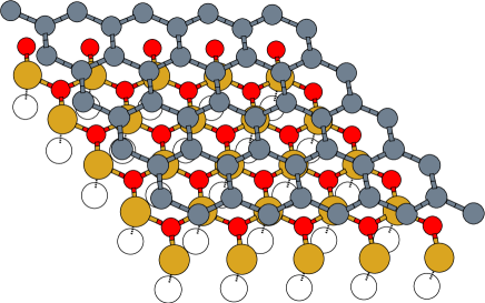
Thus we consider a stable 2D Si-O ring structure which satisfies the lattice vectors of the honeycomb structure (see Figs. 1,2). In bulk SiO2 the Si-O bond length is 1.6-1.7 Å and the bond angles are optimal at 106o, although smaller and bigger angles from 96o-126o are seen near Si/SiO2 surfacespierre . Thus there is considerable freedom with respect to bond angles and lengths. In the structures developed here, bond lengths ranging from 1.43-1.75Åare found (on total-energy minimization) as stable structures. The longer bond length is accommodated by SiO2 layers which are puckered.
The structure with valencies = 4, and 2 (and two lone pairs) for Si and O is similar to a charge-transferred N-N system where =3. The N-N system has no charge centers, where as the Si-O system has positive charges on Si and negative charges on O. It turns out that there are several possible structures which are in their energy minima. They are useful as models for the interaction of the graphene sheet with a SiO2 substrate. We have studied the following cases, depicted in Fig. 1: (i) The substrate is represented by a single stable sheet of SiO rings where the Si and O atoms sit (in the -direction) underneath the C atoms, with the carbon hexagons aligned with the Si-O rings; this will be called the ‘aligned ring structure’ (ARS). (ii)The Si atoms are under the C atoms and close to the graphene plane, while the O are below the center of the carbon hexagons and further away; this structure will be called the ‘staggered oxygen structure’ (SOS). (iii)The O atoms are under the C atoms and close to the graphene plane, while the Si are below the center of the carbon hexagons and further away from the graphene plane; this is a ‘staggered Si structure’, (SSiS). (iv)The Si-O rings are fully staggered from the carbon hexagons; i.e., a staggered-ring structure (SRS). (v) The ARS with H atoms attached to the Si-atoms and optimized to give this set of substrate models. (vi)H atoms attached to the Si in the SSiS structure and optimized to give a stable structure. Unlike the SOS and SSiS structures, this system treats the bi-partite sublattices equivalently. The SRS structure is metastable, and relaxes to SOS or SSiS if annealed using molecular dynamics, thus splitting the valley degeneracy.
Two positionings (z-locations) of the graphene sheet are studied for the ARS structure. These structures are typical of a SiO surface in that they present charged ionic centers (O and Si), as well as “dangling” bonds which are found in the structures with H atoms. That is, in these structures H atoms play a role quite different to the passivating role played by them in many model structures.

A statistical average over many such possible structures is expected in a laboratory sample. The fully microscopic calculation used here can be used within a numerical averaging over a large statistical sample of structure realizations. However, since we are studying preliminary models, such a step would be premature. Hence we examine a few structures which provide some insight into the graphene-substrate interaction.
We have used the Vienna ab initio simulation package (VASP)vasp which implements a density functional periodic plane-wave basis solution where the ionic coordinates are also equilibriated to negligibly small Hellman-Feynman forces. The projected augmented wave (PAW) pseudopotentialsvasp have been used for the carbon potential. This C pseudopotential has already been used with confidence in several graphene-type calculations (e.g., Refs. grp2, ; nieminen, ). The usual precautions with respect to -point convergence, size of the simulation cell, the extent of the plane-wave basis etc., have been takengrp2 to ensure convergence.
II.1 Bandstructure in the presence of the substrate.
In Fig. 3, we show the band-structure of several graphene-SiO systems (projected on the graphene Brillouin zone) along the KMK symmetry directions. The bands for the structures identified in Fig. 1 as SSiS, ARS, SOS and SRS, and without any H-atom attachments, are shown in the figure. The pure graphene bands are also shown (as continuous lines) in panel (a). It is clear that the fully aligned flat SiO structure is not an acceptable model for the graphene substrate. The other three models largely preserve the linear dispersion in the K direction. However, the behaviour near the K point, towards the M direction is affected by the intrusion of a flat band. The bands shown in panels (a), (c) and (d) also have a small ( 0.15 eV) energy gap which cannot be seen on the scale of the plots. However, as we discuss below, the Fermi energy itself moves by about 0.6 eV from structure to structure and hence this band-gap splitting is not significant in a real substrate where many local orientations (of the SSiS, SOS, SRS types) could occur.
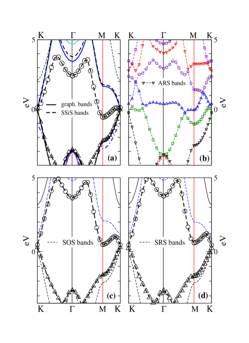
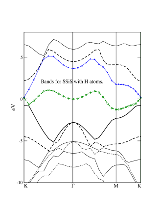
In Fig. 4 we show the bands of the SSiS system with an H atom attached to the Si atoms. This introduces an additional band criss-crossing the Fermi energy ( is set to zero in the figure), and marked as a dashed line with circles. Hence the H-atom system is not an acceptable model for graphene on a SiO substrate. Even the more satisfactory models, i.e., SSiS, SOS and SRS shown in Fig. 3 show that the graphene layer interacts with the substrate in a significant manner. Thus, the interaction between the graphene and the substrate is clearly moderated, perhaps by adsorbed atmospheric gases, and gives rise to the almost pure-graphene like behaviour experimentally observed for graphene films positioned on silica substrates.
If we consider an extended substrate including several SiO layers, as was studied by us in a different context (as in Ref. pierre, ), the charge structure of the oxygen atoms may be different in different regions. The different staggered structures present local configurations which would occur in different parts of a single substrate/graphene setup. The change in the in going from one part of the substrate where one structure (e.g., the staggered oxygen structure) prevails, to another where another structure (e.g., the staggered-Si structure) prevails locally, would be a measure of the local fluctuations on the graphene bands caused by the substrate. The calculations for the Si-O systems shown here, as well as other similar systems not discussed here, give us an variation . Moving the graphene film from 3Å to Å changes insignificantly, although there are changes in the bandstructure. Changing the alignment of the C-hexagons from the Si-O hexagons produces a change of 0.6 eV in , while the attachment and detachment of H atoms also produce effects of the same order. These calculations suggest that, when the Si-O substrate modifies the graphene bands without disrupting the DW behaviour, it could still lead to a spatially varying Fermi energy , with a variation of about 0.6 eV. We also note that the equilibrium separation between a large graphene sheet and the substrate would vary with the local substrate structure. Thus, in effect, the graphene sheet would not be flat but determined by the structural features of the substrate and the resultant interactions. It should also be noted that a sheet of graphene simply “put” on a substrate does not necessarily assume the lowest energy conformation, unless an annealing process is performed. Instead, the film would have a number of “touch points” where it would approach the substrate to some near-optimal distance (3-5 Å ). These “touch-points’ would hold the film on the substrate, while the rest of the film could be at other distances. The optimal distance of 3-5 Å is that obtained from the total energy at zero temperature, and not from the free energy, at the ambient temperature. Hence the average distances of up to 8Å , or other values, quoted in experimental studies could easily occur in different samples. nd for improved models of the SiO2 system.
Our calculations, unlike linear response or Thomas Fermi models, take account of the structural features of graphene, the essential features of the Si-O substrate, as well as the non-linear response, bound-state structure and bond-length modifications, via the self-consistent Kohn-Sham calculations used here. However, just as the Si/SiO2 interface structure of field-effect transistors required many decades of study, the graphene/SiO2 interface would also require more microscopic calculations.
III Discussion
A single-sheet of graphene gently placed on a SiO2 substrate or suspended in space is driven to deviations from perfect flatness as a consequence of well known thermodynamic constraintsmgknbr ; peierls ; mermin . Hence let us consider the wavy-graphene-sheet (WGS) model of Mayers et al.mgknbr and examine the behaviour of such a system in the low gate-voltage limit. First we note that the DW effective hamiltonian is obtained by limiting the behaviour to the neighbourhood of which is at the K points. Thus the low-energy excitations are actually associated with a high- Fourier component of the system. That is, the wave-like elastic energy perturbations of the -bonding skeleton (which are due to length scales of the order 1:10 in , where the in-plane length scale is 10 nm), would have little effect on the 2.7 eV energy scales associated with the large- regime (i.e., near the K point) effective Hamiltonian of the DW spectrum. That is, various elastic-deformation models based on extensions of the tight-binding model (fitted to the electronic excitations near the K point) will totally fail to capture the effect of the undulations of the graphene sheet. However, this point of view is not shared in Ref. [netokim, ] where a Slater-Koster tight-binding model, using the hopping matrix elements and their spatial derivatives is used. However, our experience is that such models usually fail to reproduce even the phonons in the structure. That is, the tight-binding parameters which give good electronic bands, when used in a phonon calculation do not give good phonons, and vice versa.
In our previous calculations we showed that the behaviour near the K point may survive significant charge center effects, with the proviso that the absolute value of (K) bobs up and down. We found that the for the various SiO substrates (without attached H) differed by eV. Those calculations assumed the existence of lattice periodicity in each model, with the graphene sheet located at =3-5 Å , depending on the substrate configuration. The configuration of the substrate presented to the graphene sheet (i.e., whether it is SSiS, SOS, or SRS) will differ more or less randomly, at different “touch-points”. Thus the K-point energy at each touch-point will differ, with a variation of about eV. A statistical averaging over an ensemble of such models can be carried out, inclusive of charge-charge correlations, using methods well known in astrophysicschandrasekar , plasma physicsmicrof , and in recent discussions of random charge centers acting on graphenegali .
However, we will proceed without such details as the
SiO2 models used here are rather preliminary.
We may note
that there are several effects to consider:
(i) Break-down of the lattice periodicity and the zone-edge
periodicity .
(ii)The modification of the energy at the zone edge and specifically at K.
Item (i) may be visualized as a replacement of the periodicity by an
ensemble of periodicities , and a set of folded bands with
zone edges at . The distribution would be such as to minimize
the free energy of the graphene film in the field of the substrate,
or floating free in space. In practice the film is “put” on the
substrate and its conformation may be some metastable one and not necessarily
the lowest free-energy state. The distribution of “touch-points”
defines a spatial map where the energy of the K points vary. In effect,
unlike the perfect 2D sheet, the graphene on the substrate has a
bandstructure which is a set of strongly localized (flat) states, with an average
extension in the z-direction of at the touch points.
Thus the square of the wavefunction of an electron in graphene, projected
on the - direction is no longer a -function
.
The above picture translates to the real space with the energy at the K points acquiring a a small -dependence, while the global Fermi energy of the system remains constant and aligned to the chemical potential. That is, for any measured with respect to K, we have
| (1) | |||||
| (2) |
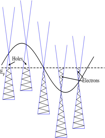
In Fig. 5 we show such an array of -dependent energy cones for graphene, for a single Fourier component of the structure factor of the graphene sheet. A sum over all such Fourier components is equivalent to a weighted sum over all possible folded bands in the reciprocal-space picture. We show only a single cone for the two degenerate valleys having a spin degeneracy as well. That is, we assume that the K, K′ degeneracy is negligible compared to the variation of the absolute value of at the length scale , as the former corresponds to length scales an order of magnitude smaller. Although the K-point energy of the cones bob up and down, the system will have a common electrochemical potential which defines the energy transport across the system when a potential is applied. Clearly, when drops below the system becomes insensitive to , and hence we can identify . Below this threshold the carrier density is determined by the waviness of the graphene sheet and not by the applied voltage which is smaller than . Given similar methods of preparation and similar conditions of observation, the parameter and the resultant carrier density would be approximately “universal” in the sense that it would lie within a limited range of possible values.
If the average -extension of the electron is , its
possible energy states would be quantized with a spectrum of
“particle in a box” like energies . The lowest of these
would correspond to the state of some effective
minimum value of the z-direction
parameter. A number of such states would be occupied, depending on .
Once falls below , one may assume that only these lowest
states, i.e., , in each cone
at or would be occupied
by the respective carriers. Thus we see that this system can indeed
reduce to just a minimal conduction channel where each channel
has a spin and valley degeneracy unless external magnetic or
electrostatic fields are present. This argument is independent
of the exact extent of and .
The z-direction bandstructure defines channels to which the Landauer-Buttiker
formula lanbut can be applied.
Taking the spin and pseudospin
degeneracy into account,
a minimum conductance of
would be expected for these systems. That is, although the
value of the threshold would not be universal, the conductance
will have a minimal universal value corresponding to the occupation
of the lowest -quantized state.
Note that this picture is quite different to the mobility-edge conductance model
of disordered semiconductorsfradkin , and closer to a model of a quasi-2D
electron gas quasi2d where the thickness varies from point to
point.
IV Conclusion
In this study we have shown that simple models of the silicon dioxide substrate can be constructed and used to give some insight into the substrate/graphene interaction. These models show that if the substrate is free of dangling bonds, a graphene layer positioned at about 4-5 Å away from the substrate preserves its DW bands. However, the energy at the K point acquires a spatial variation. The atomically thin 2-D layer effectively acquires an -extension, and the -confined states in this quasi-2D system provide the quantization necessary to define a minimum conductance of . This behaviour is different from what is expected of ideal graphene where the conductance should go to zero when the gate voltage goes to zero.
References
- (1) Mark Wilson, Physics Today 59 (2006)
- (2) K. S. Novoselov, A. K. Geim, S. V. Morozov, D. Jiang, M. I. Katsnelson, I. V. Grigorieva, S. V. Dubonos, and A. A. Firsov, Nature 438, 197 (2005);
- (3) Y. B. Zhang, Y.-W. Tan, H. L. Stormer, P. Kim, Nature (London), 438, 201 (2005)
- (4) R. Saito, M. Fujita, G. Dresselhaus and M. S. Dresselhaus, Phys. Rev. B 46 1804 (1992)
- (5) N. Tit and M. W. C. Dharma-wardana, Europhys. Lett., 62, 405 (2003); J. Gonzalez, Phys. Rev. Lett. 88, 76403 (2002).
- (6) J. M. Pereira Jr., V. Mlinar, F. M. Peeters, and P. Vasilopoulos, Phys. Rev. B 74, 045424 (2006)
- (7) Ph. Avouris, J. Chen, Materials Today 9, 46 (2006)
- (8) Pierre Carrier, Laurent Lewis, and M. W. C. Dharma-wardana, Phys. Rev. B 65 165339 (2002)
- (9) D. P. DiVincenzo and E. J. Mele, Phys. Rev. B 29, 1685 (1984)
- (10) http://arxiv.org/pdf/cond-mat/0702117
- (11) N. H. Shon and T. Ando, J. Phys. Soc. Jpn. 67, 2241 (1998)
- (12) M. L. Katsnelson, Euro. Phys. J. B51, 157 (2006); K. Ziegler, Phys. Rev. Lett. 97,266802 (2006)
- (13) K. Nomura and H. H. MacDonald Phys. Rev. Lett. 96 256602 (2006)
- (14) J. C. Meyer, A. K. Giem, M. I. Katsnelson, K. S. Novoselov, T. J. Booth, and S. Roth, http://arxiv.org/pdf/cond-mat/0701379
- (15) R. E. Peierls, Helv. Phys. Acta 7 81 (1934)
- (16) N. D. Mermin, Phys. Rev. 176 250 (1968)
- (17) N. M. R. Peres, F. Guinea and A. H. Castro Neto, Phys. Rev.B 72, 174406 (2005); M. A. H. Vozmediano, M. P. Lopez-Sancho, T. Stauber and F. Guinea, Phys. Rev. B 72, 155121 (2005); N. M. R. Peres, F. Guinea and A. H. Castro Neto, Phys. Rev. B 73,125411 (2006)
- (18) T. O. Wehling, A. V. Balatsky, M. I. Katsnelson, A. I. Lichtenstein, K. Scharnberg, R. Wiesendanger, cont-mat/0609503
- (19) M. W. C. Dharma-wardana, Phys. Rev. B 75, 075427 (2007)
- (20) F. Varchon, R. Feng, J. Hass, X. Li, B. N. Nguyen, C. Naud, P. Mallet, J.-Y. Veuillen, C. Berger, E. H. Conrad, and L. Magaud, http://arxiv.org/pdf/cond-mat/0702311
- (21) Yuchen Ma, A. S. Foster, A. V. Krasheninnikov, and R. M. Nieminen, Phys. Rev. B 72, 205416 (2005); B. I. Danlap and J. C. Boettgerm J. Phys. B: At. Mol. Phys. 29, 4907 (1996)
- (22) Regarding the VASP code, see G. Kress, J. Furthmüller and J. Hafner, http://cms.mpi.univie.ac.at/vasp/
- (23) M. W. C. Dharma-wardana, Solid St. Com. 140, 4 (2006)
- (24) A. H. Castro Neto, Eun-Ah Kim, cond-mat/0702562
- (25) S. Chandrasekhar, in Selected Papers on Noise and Stochastic Processes, edited by N. Wax (Dover, New York, 1954).
- (26) F. Perrot and M. W. C. Dharma-wardana, Physica A (Stat. Phys.) 134 231 (1985)
- (27) M. Büttiker, in Electronic Properties of Multilayers and Low-dimensional Semi-conductor Structures, edited by J. M. Chamberlain (Plenum, New York, 1990), p. 297
- (28) E. Fradkin, Phys. Rev. B 33, 3263-3268 (1986)
- (29) M. W. C. Dharma-wardana, Phys. Rev. B 72, 125339 (2005)