Even-odd effect in Andreev Transport through a Carbon Nanotube Quantum Dot
Abstract
We have measured the current()-voltage() characteristics of a single-wall carbon nanotube quantum dot coupled to superconducting source and drain contacts in the intermediate coupling regime. Whereas the enhanced differential conductance due to the Kondo resonance is observed in the normal state, this feature around zero bias voltage is absent in the superconducting state. Nonetheless, a pronounced even-odd effect appears at finite bias in the sub-gap structure caused by Andreev reflection. The first-order Andreev peak appearing around is markedly enhanced in gate-voltage regions, in which the charge state of the quantum dot is odd. This enhancement is explained by a ‘hidden’ Kondo resonance, pinned to one contact only. A comparison with a single-impurity Anderson model, which is solved numerically in a slave-boson meanfield ansatz, yields good agreement with the experiment.
pacs:
74.78.Na,74.45.+c,73.63.Kv,73.21.La,73.23.Hk,73.63.FgThere is a growing interest in the exploration of correlated charge transport through nanoscaled low-dimensional systems involving both superconductors and normal metals Choi-Review ; Ralph ; Morpurgo ; Glazman-Sdot ; MAR-Atom-Contact ; Review-Bouchiat . The penetration of the pair amplitude from a superconductor (S) into a normal metal (N), the proximity effect, is a manifestation of correlated charge transport mediated by Andreev processes taking place at the S-N interface Proximity-Effect and leading in S-N-S junctions to the Josephson effect Josephson-Likharev and sup-gap current peaks due to multiple Andreev reflection (MAR) Octavio . The superconducting proximity effect has been studied in great detail in the mesoscopic size regime of diffusive, but phase coherent conductors Meso-Supra . Andreev transport has also been the key quantity in experiments elucidating charge transport in single atom contacts MAR-Atom-Contact ; MAR-Cuevas . On the other hand, Andreev transport through a quantum dot coupled to superconductors, is just emerging now Buitelaar-SKondo ; Buitelaar-MAR ; Graeber-SKondo ; Herrero-Jorgensen-Wernsdorfer . If the dot is weakly coupled to the leads, Andreev processes are suppressed by the charging energy of the dot Ralph ; S-Resonance-S-Alfredo ; S-Resonance-S-Wendin . If the dot is sufficiently small, size quantization takes place, forming a quantum dot (QD) with discrete eigenstates (‘levels’) at energies . Transport then occurs through individual levels Ralph . Since the level ‘positions’ , and sometimes also the coupling strengths of the levels to both source and drain contacts , can be tuned through gate voltages, a physically tunable model system of the Anderson ‘impurity problem’ is realized. With one electron on the QD (half-filling), a many-electron ground-state forms, involving both the dot-state and conduction electrons from the leads in an energy window given by the the Kondo temperature Goldhaber-Gordon ; Kondo-Effect . In this Kondo regime, which can be observed if is not too small, a resonance pinned at the Fermi energy of the leads forms (Kondo resonance). If superconducting contacts are used instead of normal ones, the additional pair-correlation in the leads competes with the Kondo correlations on the QD Choi-Review ; Glazman-Sdot ; Schwab-SB-SKondo ; Bergeret ; Cuevas-Kondo-SN ; Kondo-S . It has been found recently in experiments using carbon nanotubes (CNTs) as QDs, that there is an interesting cross-over occurring at . If , the Kondo correlations are suppressed, whereas they persist in the opposite regime, opening a highly conducting channel for the Josephson effect Buitelaar-SKondo ; Glazman-Sdot . CNTs are ideally suited for the realization of such systems, because CNTs can a) act as well controlled QDs in different transport regimes Review-Sapmaz , including the Kondo regime Kondo_CNT , and b), different types of contacts can be realized, including superconducting ones Morpurgo ; Review-Bouchiat ; Buitelaar-SKondo ; Buitelaar-MAR ; Graeber-SKondo ; Herrero-Jorgensen-Wernsdorfer . Similar physics can be addressed with QDs fabricated in semiconducting nanowires contacted to S contacts Nanowires .
We here report on measurements of the non-equilibrium (finite-bias) transport through a single-wall carbon nanotube QD with S contacts in the most interesting regime of intermediate coupling, where Kondo correlations are of similar magnitude as superconducting ones. We have found a pronounced even-odd effect in the MAR structure.
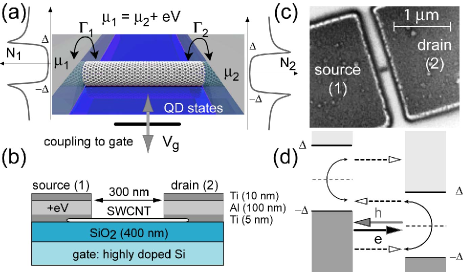
Single walled carbon nanotubes were grown by chemical vapor deposition on highly-doped Si wafers with a nm layer of thermal oxide on top, using Fe particles as catalysts 1998-Kong ; Comment-CVD . Individual single-wall carbon nanotubes (SWCNTs) were localized with a scanning electron microscope and contacted to supercondcuting source and a drain electrodes using e-beam lithography, see Fig. 1. The evaporated contacts consist of a Ti(nm)/Al(nm)/Ti(nm) tri-layer, where Ti serves as an adhesion and cap-layer. Al is the actual superconductor with a bulk critical temperature of K. In its thin film form, we rather measure a of K, which corresponds to a BCS gap-parameter of meV. We drive the Al contacts into the normal state by applying a small perpendicular magnetic field of T. The substrate is contacted to a third terminal in order to establish a backgate. We measure the differential source(1)-drain(2) conductance as a function of source-drain and gate-voltage . This is achieved by superposing an ac-voltage V on and measuring the corresponding ac current with a current-voltage converter and a lock-in amplifier. Several devices were fabricated and tested at room temperature and at K. Here, we focus on a particular interesting device which we selected and measured in a dilution refrigerator. This device has been studied over a large window and displays single-electron charging with addition energies in the range of meV. In the following we will focus on a confined gate-voltage regime.
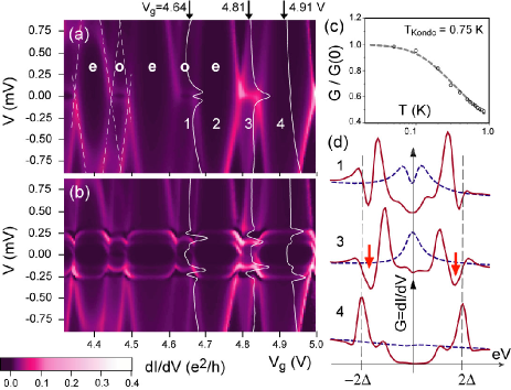
Fig. 2 shows the main measurements we will be focusing on in the following. Visible is in (a) a plot in the normal state (n-state) and the corresponding one in the superconducting state (s-state) in (b). In the n-state a sequence of larger and smaller Coulomb blockade (CB) diamonds are seen (dashed lines), corresponding to a sequence of nearly equidistantly spaced levels on the SWNT-QD, which are filled sequentially. The number of electrons on the dot therefore alternates in the ground-state between odd and even CNTs-Odd-Even . It is also seen that the conductance around zero bias is suppressed and featureless in the even valleys, but is increased assuming structure in the odd ones. In the CB diamond labelled 3, there is a pronounced peak at , suggesting the appearance of a Kondo resonance. Indeed, the dependence of the linear on temperature (Fig. 2c), measured in the middle of this valley, follows the expected dependence TK-of-T-dependence with a Kondo temperature of K. In the other odd valleys, the Kondo resonances are split by meV Comment1 . The origin of this splitting is at present not known, but could be due to exchange with ferromagnetic catalyst particles or another tube (if the present one is a small bundle or contains more than one shell) Kondo-Splitting .
The n-state data can be used to deduce a number of parameters. The source, drain and gate capacitances are aF and aF, leading to a gate-coupling of , where . The charging energy and the level spacing are in the range of meV and meV, respectively. Whereas this SWNT-QD is nearly symmetric in its electrostatic coupling, it is quite asymmetric in its electronic one. The total level broadening amounts to meV with an asymmetry of . This asymmetry is deduced from the measured current peaks in at the border of the CB diamonds at finite bias and is in agreement with the reduced low temperature zero-bias of the Kondo ridge 3, amounting to .
Looking next at the s-state, we see that the major changes in the are confined to a voltage band of meV meV, corresponding to . Above , i.e. , quasiparticle current is possible and the main modification is caused by the peak in the superconducting density-of-state (DOS) Ralph ; MAR-Cuevas , leading to a peak-like feature in . Due to the gap in the DOS, first order processes are however suppressed below . Depending on the transmission probability S-Resonance-S-Alfredo ; S-Resonance-S-Wendin ; Buitelaar-MAR , higher order Andreev processes can contribute. The first order Andreev process, for example, results in a peak-like structure in the vicinity of . Due to the higher order, the first Andreev peak and all subsequent ones are usually smaller than the quasiparticle one. Both the dominant and the smaller peak, as well as the suppressed in the s-state are best visible in the middle of an even charge state (even valley), see e.g. curve labelled 4 in Fig. 2d. In contrast, in the odd charge states, the feature is not present or does not appear at . Starting to view the data from large bias voltage, the first peak appears closer to rather than , with a preceding negative (NDR), see curve labelled 3 in Fig. 2d. Hence, there is a striking even-odd asymmetry in the finite-bias features in the s-state which is not caused by the CB resonance at the edges of adjacent charge states, where the situation is expected to be more complex S-Resonance-S-Alfredo ; S-Resonance-S-Wendin . The even-odd alteration of the MAR structure suggest a relation to Kondo physics. To model this, we first extract important parameters from an analysis of the data in the middle of an even valley where Kondo correlations are absent.
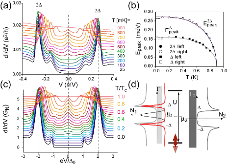
Fig. 3a-c discusses the temperature dependence of in the middle of the even charge state; (a) shows the measurement taken in valley 4 of Fig. 2 and (c) is a model calculation. The experiment displays pronounced quasiparticle current peaks at , and weaker MAR peaks at . The evolution of with temperature are shown in Fig. 3b together with an approximate BCS gap function , where we used the BCS value for , which amounts to meV for a of K. We then obtain and for the two peaks. The slight increase of above the expected value of is not unusual. We will be using the value meV as the zero-T gap parameter in the following. The relevant parameters expressed in units of are then: , , and . The zero-bias peak in Fig. 3a, appearing at intermediate temperatures, can be explained by direct tunneling of quasiparticles thermally activated across the gap.
The good agreement with the BCS relation of the peak-positions motivates the modelling of the using the BCS-DOS in the leads. Although we would have to use a theory describing resonant tunneling between two superconductors, such as the one from Levy Yayati et al. S-Resonance-S-Alfredo , a simple tunneling picture suffices Tinkham , because the resonant levels are far away from the electrochemical potential of the electrodes in the middle of a charge state. The subgap current is treated in the same approximation using MAR-Cuevas . To obtain a reasonable fit, the BCS-DOS has been convoluted with a Gaussian of width . A quite good agreeement is found with .
We now turn our attention to the odd charge states. We point out, that the zero-bias high- Kondo ‘ridge’, which is associated with the Kondo resonance and visible in the n-state, is not seen in the s-state. This is consistent with a Kondo temperature that is smaller than , i.e. Glazman-Sdot ; Buitelaar-SKondo . Although the Kondo resonance is not visible in the s-state, we suspect it to be responsible for the even-odd asymmetry of the -feature in the s-state.
In the Kondo regime, the single spin on the QD in the odd state is screened by exchange with conductance electrons from the leads. If the quasiparticles are bound in Cooper pairs in the leads, the Kondo temperature is renormalized, assuming a smaller value . This renormalization is sensitive on the actual parameters and . Due to the asymmetry, it may happen that a Kondo resonance with a reduced width forms on the contact with the larger , whereas on the other one it is suppressed. This is illustrated in Fig. 3d.
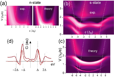
We modelled this scenario considering a single-level Anderson Hamiltonian with interaction coupled to source and drain contacts. The experimentally deduced ’s, including the strong asymmetry were used. The calculation is based on a slave-boson mean-field treatment of this interacting problem Bergeret . The result of the comparison is shown in Fig. 4: (a) corresponds to the n-state and (b) and (c) to the s-state. Despite this simple model, the agreement is surprisingly good. It is remarkably good in the normal state, shown in Fig. 4a. In the s-state, the dominance of the -like feature in the odd valley is clearly present, as is a similar cross-over from odd to even filling. There are also some differences: in the experiment the -feature bends to larger -values in the middle of the odd state, whereas this feature is rather flat in the calculation.
In conclusion we have discovered a pronounce even-odd effect in the (multiple) Andreev structure in transport through a QD with superconducting contact. This effect is driven by a Kondo resonance pinned to one contact only and defines a new regime. Whereas a high conductance channel from source to drain, driven by Kondo correlations, persists in the supercondcuting state if , this channel is greatly suppressed in the opposite limit. In the intermediate regime , and in particular for asymmetric dot-electrode couplings, the (partial) Kondo-screening of the ‘impurity’ spin may occur on one electrode only. It would be interesting to explore the ‘robustness’ of this feature in model calculation and to fabricate similar QDs with tunable electrode couplings.
I Acknowledgements
We have profited from fruitful discussions with E. Scheer, W. Belzig, and V. Golovach. We thank J. Gobrecht (PSI) for providing the oxidized Si substrates. The work at Basel has been supported by by the Swiss National Science Foundation, the NCCR on Nanoscale Science, FP6-RTN DIENOW and EU-FP6-IST project HYSWITCH.
References
- (1) For a recent review, see: Mahn-Soo Choi, Int. J. of Nanotechn. 3, 216 (2006).
- (2) L. I. Glazman and K. A. Matveev, JETP Lett. 49, 659 (1989).
- (3) D. C. Ralph, C. T. Black, and M. Tinkham, Phys. Rev. Lett. 74 3241 (1995);
- (4) A. F. Morpurgo, J. Kong, C. M. Marcus, and H. Dai, Science 286, 263 (1999).
- (5) for a review, see: N. Agrait, A. Levy Yeyati, J. M. van Ruitenbeek, Phys. Rep. 377, 81 (2003).
- (6) A. Yu. Kasumov, R. Deblock, M. Kociak, B. Reulet, H. Bouchiat, I. I. Khodos, Yu. B. Gorbatov, V. T. Volkov, C. Journet, and M. Burghard, Science 284, 1508 (1999);
- (7) P. G. de Gennes, Rev. Mod. Phys. 36, 225 (1964); A. F. Andreev, Sov. Phys. JETP 19, 1228 (1964);
- (8) B. D. Josephson Rev. Mod. Phys. 36, 216 (1964); K. K. Likharev, Rev. Mod. Phys. 51, 101 (1979).
- (9) M. Octavio, M. Tinkham, G. E. Blonder, and T. M. Kalpwijk, Phys. Rev. B 27, 6739 (1983).
- (10) For a review, see: special issue on Mesoscopic Superconductivity, Superlattices and Microstructures 25, issues 5/6, edited by P. F. Bagwell (1999).
- (11) J. C. Cuevas, A. Martín-Rodero, and A. Levy Yeyati Phys. Rev. B 54, 7366 (1996).
- (12) M. R. Buitelaar, T. Nussbaumer, C. Schönenberger, Phys. Rev. Lett. 89, 256801 (2002).
- (13) M. R. Buitelaar, W. Belzig, T. Nussbaumer, B. Babic, C. Bruder, and C. Schönenberger, Phys. Rev. Lett. 91, 057005 (2003).
- (14) M. R. Gräber, T. Nussbaumer, W. Belzig, and C. Schönenberger, Nanotechnology 15, S479-82 (2004).
- (15) P. Jarillo-Herrero, J. A. van Dam, and L. P. Kouwenhoven, Nature 439, 953 (2006); H. I. Jorgensen, K. Grove-Rasmussen, T. Novotný, K. Flensberg, and P. E. Lindelof, Phys. Rev. Lett. 96, 207003 (2006); J.-P. Cleuziou, W. Wernsdorfer, V. Bouchiat, T. Ondarcuhu, M. Monthioux, Nature Nanotechnol. 1, 53 (2006).
- (16) A. Levy Yeyati, J. C. Cuevas, A. López-Dávalos, and A. Martín-Rodero, Phys. Rev. B 55, R6137 (1997).
- (17) G. Johansson, E. N. Bratus, B. Verkin, V. S. Shumeiko, and G. Wendin, Phys. Rev. 60, 1382 (1999).
- (18) D. Goldhaber-Gordon, H. Shtrikman, D. Mahalu, D. Abush-Magder, U. Meirav, and M. A. Kastner, Nature 391, 156 (1998).
- (19) M. Pustilnik, L. Glazman, J. of Phys.: Cond. Matter 16, R513 (2004).
- (20) P. Schwab and R. Raimondi, Phys. Bev. B 59, 1637 (1999); S. Y. Liu and X. L. Lei, Phys. Rev. B 70, 205339 (2004).
- (21) F. S. Bergeret, A. Levy Yeyati, and A. Martín-Rodero, Phys. Rev. B 74, 132505 (2006).
- (22) J. C. Cuevas, A. Levy Yeyati, and A. Martín-Rodero, Phys. Rev. B 63, 094515 (2001).
- (23) A. Levy Yeyati, A. Martín-Rodero, and E. Vecino, Phys. Rev. Lett. 91, 266802 (2003); Y. Avishai, A. Golub, and A. D. Zaikin, Phys. Rev. B 67, 041301 (2003).
- (24) S. Sapmaz, P. Jarillo-Herrero, L. P. Kouwenhoven, H. S. J. van der Zant, Semicond. Sci. Technol. 21, S52 (2006).
- (25) J. Nygard, D, H. Cobden, P. E. Lindelof, Nature 408, 342 (2000);
- (26) Y.-J. Doh, J. A. van Dam, A. L. Roest, E. P. A. M. Bakkers, L. P. Kouwenhoven, and S. De Franceschi, Science 309, 272 (2005); J. A. van Dam, Y. V. Nazarov, E. P. A. M. Bakkers, S. De Franceschi, and L. P. Kouwenhoven, Nature 442, 667 (2006).
- (27) J. Kong, H. T Soh, A. M. Cassel, C. F. Quate, and H. Dai, Nature 395, 878 (1998).
- (28) at o in a mixture of H2 and CH4 with flow rates of and l/min, respectively.
- (29) D. H. Cobden, M. Bockrath, P. L. McEuen, A. G. Rinzler, R. E. Smalley, Phys. Rev. Lett. 81, 681 (1998); D. H. Cobden, and J. Nygard, Phys. Rev. Lett. 89, 046803 (2002).
- (30) D. Goldhaber-Gordon et al., Phys. Rev. Lett. 81, 5225 (1998).
- (31) This splitting of the Kondo resonace is much larger than the Zeeman splitting due to the applied magnetic field of T, amounting to eV.
- (32) H. Jeong, A. M. Chang, and M. R. Melloch, Science 293, 2221 (2001); A. N. Pasupathy, R. C. Bialczak, J. Martinek, J. E. Grose, L. A. K. Donev, P. L. McEuen, and D. C. Ralph, Science 306, 86 (2004); J. Nygard, W. F. Kohl, N. Mason, L. DiCarlo, and C. M. Marcus, cond-mat/0410467; M. G. Vavilov and L. I. Glazman, Phys. Rev. Lett. 94, 086805 (2005).
- (33) M. Tinkham, Introduction to Superconcuctivity (MacGraw Hill, New York 1996).