Displacements of domain walls in electroded ferroelectric single crystals:
the effect of surface layers on restoring force
Abstract
Macroscopic properties of ferroelectric samples, including those in form of thin films, are, to large extent, influenced by their domain structure. In this paper the free energy is calculated for a plate-like sample composed of nonferroelectric surface layers and ferroelectric central part with antiparallel domains. The sample is provided with electrodes with a defined potential difference. The effect of applied field and its small changes on the resulting domain structure is discussed. This makes it possible to determine the restoring force acting on domain walls which codetermines dielectric and piezoelectric properties of the sample. Calculations of the potential and free energy take into account interactions of opposite surfaces and are applicable also to thin films.
I Introduction
It is known that samples of ferroelectric single crystals often posses a surface layer whose properties differ from those of the bulk. It may be a layer produced during the growth of a crystalline plate or produced during the preparation of a plate-like sample. Many observations gave evidence to the fact that such a layer is either nonferroelectric or does not take part in the switching process of the internal part; in any case its permittivity is believed to differ from that of a homogeneous sample in the ferroelectric phase. Its existence is expected to greatly influence macroscopic properties of bulk samplesArtA1:Miller ; ArtA1:Drougard ; ArtA1:Muser ; ArtA1:Callaby as well as of thin films.ArtA1:Tagantsev In this paper two such consequences are investigated. First we reconsider the problem of equilibrium domain structure in a ferroelectric sample possessing a surface layer, previously discussed by Bjorkstam and Oettel.ArtA1:Bjorkstam Second, we evaluate the restoring force acting on domain walls due to the layer; this will make it possible to estimate the extrinsic contributions to permittivity, piezoelectric coefficients and elastic compliances of a ferroelectric sample. Investigations of crystals of the KDP family revealed the existence of huge wall contributions to these properties.ArtA1:Nakamura ; ArtA1:Stula
In previous papers on a related subjectArtA1:Drougard , depolarizing field was considered as the source of energy which slows down the motion of a single domain wall in a dc electric field, as the wall departs from its original position by substantial distances. In contrast to such models we investigate very small deviations of walls forming a regular domain pattern.
II Geometry, variables and energy of the system
We consider a plate-like electroded sample of infinite area with major surfaces perpendicular to the ferroelectric axis . Central ferroelectric part with antiparallel domains (2.) is separated from the electrodes (0.), (4.) by nonferroelectric layers (1.), (3.) (see Fig. II). The spatial distribution of the electric field is determined by the applied potential difference and by the bound charge div on the boundary of ferroelectric material, where stands for spontaneous polarization. Geometrical, electrical and material parameters of the system are shown in Fig. II.
We further introduce the symbols
[r][t]
![[Uncaptioned image]](/html/cond-mat/0702303/assets/x1.png) Geometry of the model
Geometry of the model
and several geometrical parameters:
the domain pattern factor
and the asymmetry factor
The ferroelectric material itself is approximated by the equation of state
where is the spontaneous polarization along the ferroelectric axis. This linear approximation limits the validity of our calculations to the temperature region not very close below the transition temperature . Domain walls are assumed to have surface energy density and zero thickness.
The Gibbs electric energy of the system includes the domain wall energy, the electrostatic energy whose density is and the work performed by external electric sources , where is the charge on positive electrode. First, Laplace equations have to be solved for electric potentials in the bulk and in the surface layers, fulfilling the requirement of potential continuity as well as conditions of continuity of normal components of and tangential components of . A rather cumbersome calculation leads to the following formula for Gibbs electric energy per unit area of the system (in ):
| (1) |
The first term represents domain wall contribution while the last one is the depolarization energy. In the second term we recognize the effect of layers (1.) and (3.) and of the applied voltage.
Let us compare expression with formulae deduced and used in previous papers. For and , and the system goes over into an isolated ferroelectric plate with “neutral” domain structure, placed in vacuum. In this case the equation (1) reduces to the expression given by Kopal et al.ArtA1:Kopal for ferroelectric plates of finite thickness in which the interaction of the two surfaces is accounted for. If the plate is thick this interaction can be neglected and Eq. (1) simplifies to the classical formula of Mitsui and FuruichiArtA1:Mitsui (cf. Eq. (9) in Ref. ArtA1:Kopal ) which is often used to determine the value from the observed width of domain patterns. Finally, in the limit of our formula (1) should converge to the expression deduced by Bjorkstam and Oettel.ArtA1:Bjorkstam In fact this is not the case and it appears that the electric displacement as expressed in Ref. ArtA1:Bjorkstam does not satisfy all boundary conditions.
III Equilibrium domain structure for
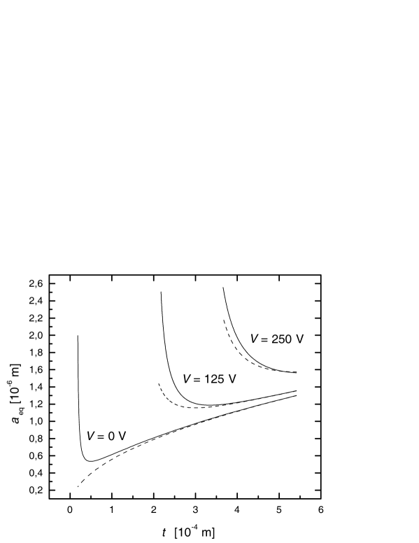
If the system is short-circuited, the equilibrium domain pattern is symmetric, i.e. . The shape factor and from it also the value of can be found by numerical methods. As an example, the full lines in Fig. 1 shows the dependence at constant and different values of potential difference . As it was shown in the previous paperArtA1:Kopal , the critical thickness can be defined by the formula
so that for the interaction energy of sample surfaces can be neglected. Then the minimum energy occurs for
| (2) |
and the dependence in this approximation is shown by a dashed line with V in the Fig. 1. The approximate results in the Fig. 1 with V and V are based on Eqs. (3) and (4). In these numerical calculations we have used the following values which roughly apply to crystals of below the transition temperature: , , , . The value is often considered typical for ferroelectrics.
IV Response of domain structute to external electric field
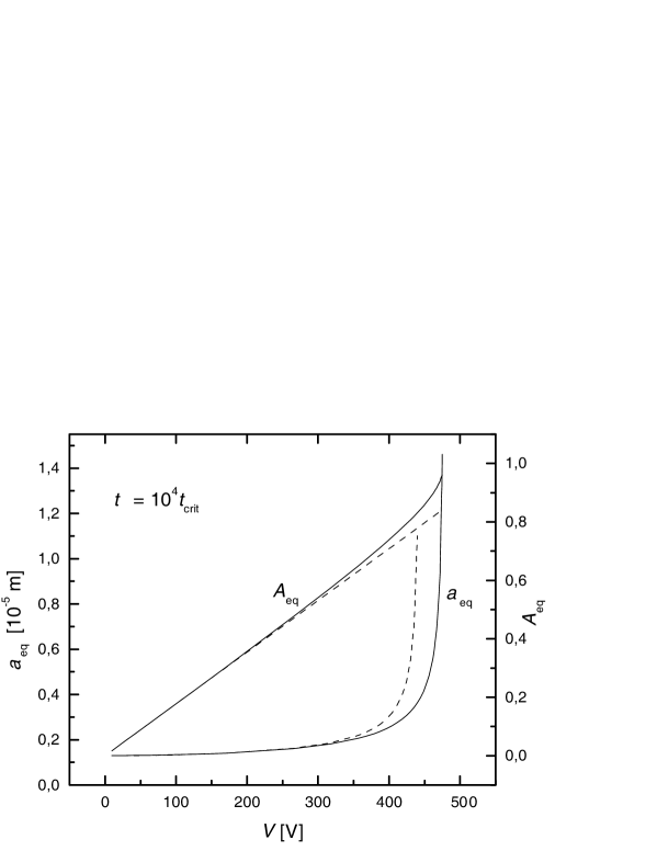
When an external potential difference is applied, the asymmetry parameter becomes nonzero and at the same time the period changes. Both these quantities can be found again by determining the minimum of given by Eq. (1) numerically. Full lines in Fig. 2 demonstrate both these dependencies for the following numerical values: , . Starting from a certain applied voltage the domain spacing grows very fast with increasing . To discuss the macroscopic properties of the sample such as permittivity, the dependence is more important. We recognize that in a considerable region of the applied voltage this dependence is almost linear.
V Extrinsic permittivity
The nonzero value of the asymmetry parameter means that an extra bound charge is deposited on the electrodes due to the domain wall shifts and this in turn represents an increase of effective permittivity of the whole system crystal plus both surface layers. The increase of the electrostatic energy when domain walls leave their original equilibrium positions for serves as the source of a restoring force when field is again reduced to zero. The calculations show that the effective permittivity defined by the total capacitance per unit area equals
| (5) |
In this formula the first term on the right-hand side represents the intrinsic part of permittivity, given by linear dielectric response of the sample and of the surface layers when domain walls are kept at rest. The second term is the contribution of domain walls displacement to effective permittivity, often referred to as extrinsic part of permittivity.
VI Discussion
Numerous data are available on domain wall contributions to permittivity in single crystals of ferroelectrics and also on extrinsic contributions to piezoelectric coefficients in ferroelectrics which are simultaneously ferroelastic. Our calculations indicate that depolarizing energy can be an effective source of restoring force whose existence is a condition for such contributions. In fact since the model assumes a regular system of planar domain walls, it is suitable in particular for ferroelastic ferroelectrics such as crystals of the KDP family in which a dense pattern of domains is known to exist.ArtA1:Fouskova ; ArtA1:Bornarel It was found that in a wide temperature range below the Curie point of crystals of and deuterated KDP, the piezoelectric coefficient is greatly enhanced compared to its expected value for single domain samples.ArtA1:Shuvalov Recently, this was confirmed by simultaneous measurements of permittivity , elastic compliance and piezoelectric coefficient of . A thorough discussion of in this case will be the subject of a forthcoming paper Kopal et al.. Here we comment on the extrinsic part of . For simplicity, let us assume that . This is not an unreasonable assumption since the assumed surface layer for KDP-type samples can be supposed to have a similar chemical composition as the bulk. Then the extrinsic part of Eq. (5) reduces to
Numerically, the second term in the brackets represents a small correction to the first term when approximations (3) and (4) are valid. If it is neglected, we obtain as an approximation
| (6) |
This shows that a very thin surface layer can lead to a considerable extrinsic enhancement of permittivity. Nevertheless, the simple implication: is not correct, because the assumptions needed for validity of (3), (4), (5) and (6) are violated if is small enough.
A more general formulation of the restoring force can be used to calculate the extrinsic part of for the same geometry of domains. In a recent paperArtA1:sidorkin Sidorkin deduced the dispersion law of wall contributions to permittivity, however, in his treatment the existence of a surface layer is not explicitly considered.
It was shown beyond any doubt that small motions of domain walls are responsible for a considerable enhancement of permittivity and piezoelectric coefficients in poled ferroelectric ceramics.ArtA1:Arlt1 ; ArtA1:Zhang One of the sources of the restoring force responsible for these wall contributions is the elastic energy at grain boundaries.ArtA1:Arlt2 Since these boundaries may differ in chemical composition from the bulk of grainsArtA1:Heydrich , surface layers can be expected to form so that the mechanism proposed in the present paper may also play a role in ceramic samples.
References
- (1) R. C. Miller and A. Savage, J. Appl. Phys. 32 (1961) 714.
- (2) M. E. Drougard and R. Landauer, J. Appl.Phys. 30 (1959) 1663.
- (3) H. E. Müser, W. Kuhn and J. Albers, phys. stat. sol. (a) 49 (1978) 51.
- (4) D. R. Callaby, J. Appl. Phys. 36 (1965) 2751.
- (5) A. K. Tagantsev, C. Pawlaczyk, K. Brooks and N. Setter, Integrated ferroelectrics 4 (1994) 1.
- (6) J. L. Bjorkstam and R. E. Oettel, Phys. Rev., 159 (1967) 427.
- (7) E. Nakamura, Ferroelectrics, 135 (1992) 237.
- (8) M. Štula, J. Fousek, H. Kabelka, M. Fally and H. Warhanek, J. Korean Phys. Soc. (Proc. Suppl.), 32 (1998) 758.
- (9) A. Kopal, T. Bahník and J. Fousek, Ferroelectrics 202 (1997) 267.
- (10) T. Mitsui and J. Furuichi, Phys. Rev., 90(2) (1953) 193.
- (11) A. Fousková, P. Guyon and J. Lajzerowicz, Compt. Rend. 262(13) (1966) 907.
- (12) J. Bornarel, Ferroelectrics 71 (1987) 255.
- (13) L. A. Shuvalov, I. S. Zheludev, A. V. Mnatskanyan and T. Z. Ludupov, Bulletin Acad. Sci. USSR Phys. Ser. 31 (1967) 1963.
- (14) A. S. Sidorkin, J. Appl. Phys. 83 (1998) 3762.
- (15) G. Arlt and H. Dederichs, Ferroelectrics 29 (1980) 47.
- (16) Q. M. Zhang, H. Wang, N. Kim and L. E. Cross, J. Appl. Phys. 75(1) (1994) 454.
- (17) G. Arlt and N.A. Pertsev, J. Appl. Phys. 70 (1991) 2283.
- (18) H. Heydrich and U. Knauer, Ferroelectrics 31 (1981) 151.