Dependence of band structures on stacking and field in layered graphene
Abstract
Novel systems of layered graphene are attracting interest for theories and applications. The stability, band structures of few-layer graphite films, and their dependence on electric field applied along the c-axis are examined within the density functional theory. We predict that those of Bernal type and also rhombohedral type tri- and tetra-layer graphite films exhibit stability. The rhombohedral-type systems including AB-bilayer, show variable band gap induced by perpendicular electric field, whereas the other systems such as the Bernal-type films stay semi-metallic.
keywords:
A. Thin films , C. Crystal structure and symmetry , D. electronic band structure, D. dielectric responsePACS:
73.63.Bd , 73.43.Cd , 81.05.Uw1 Introduction
Amongst the variety of allotropes of carbon over the full range of dimensionality, two-dimensional (2D) crystals consist of a single or few graphite layers have been stimulating scientist’s interest in theories and in possibility for novel applications. The observations of anomalous electric field effect on Hall coefficient[1], unconventional integer quantum Hall effects in monolayer[2] and bilayer graphite[3] have been enabled by recent achievement of high quality preparation of the ultra-thin graphitic films[1].
These unusual electronic properties are believed to originate in unusual band structures near Fermi level of graphene[4], a graphitic monolayer, and of its layered structures. Graphene has a direct zero energy gap between -linear bands crossing at each corner (K point) of the 2D hexagonal Brillouin zone. The charge carriers in graphene therefore are massless Dirac fermions, which leads to shifted Hall plateaus[2]. While the chiral parabolic band dispersion in AB-stacked bilayer graphene was found to give another new type of Hall effect[3].
Very recently several groups have reported calculated low-energy band structures of AB-stacked graphene layers using Tight-Binding (TB) models for band at zero electric field[5] and with field perpendicular to the layer[6]. In the latter, they examined field induced band gap in AB-bilayer and found interesting band deformation in ABA- and ABAB-stacked systems.
However, reliable TB parameters are only available for the limited equilibrium structures. Furthermore, the self-consistency should be crucial for studying their response against the electric field, because of the induced charge redistributions or polarizations as pointed out in the studies of dielectric function of graphite[7]. Properties of non-AB-type systems must be worth examining, because 16 percent of the natural and synthesized graphite are rhombohedral (ABC-stacked) with other 4 percent disordered.
The purpose of the present study is to examine the band structures and interlayer binding energy of few-layer graphite (FLG) within the density functional theory (DFT) with the local density approximation (LDA), focusing on the effects of stacking sequence and external electric field.
2 Methods
We employed the CPMD pseudopotential planewave code[8] as the ab initio total energy and band calculations in the present study. Goedecker-Teter-Hutter pseudopotential for carbon together with Padé approximant LDA exchange-correlation potential were used[9]. A sufficiently large planewave cutoff of 120 Ry was used to achieve convergence for the wavefunctions, and 480 Ry for the density. The Monkhorst-Pack[10] special -point mesh of within the first Brillouin zone (BZ) was used in the density optimizations.
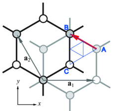
Two-dimensional (2D) structures of two up to four graphene layers are simulated using 3D hexagonal unit cells defined by primitive lattice vectors (see Fig. 1) , , and with the optimized parameter Å. and , and Å for bi-, tri- and tetra-layer systems, respectively, which ensure at least 10 Å of vacuum separations along c-axis.
The primitive reciprocal vectors in the basal plane are , , and the corners of the first Brillouin zone are labeled “K” which are given by plus the arbitrary reciprocal vectors.
We examine the stability of FLG systems using the total energy calculation within the DFT-LDA. It is known that DFT-LDA fails to describe long-range dispersion (van der Waals) interactions, but it well describes the short-range repulsion [11] and predicts the ground state structure and interlayer binding energy [12] in good agreement with experiments. Furthermore, Lennard-Jones type van der Waals energy does not make much difference between a discreat-atom and continuum models for graphitic plane. The zero-point phonon energy may not be important in the present calculations, since the influence of stacking configuration on it is considered to be negligible.
3 Structures of FLGs
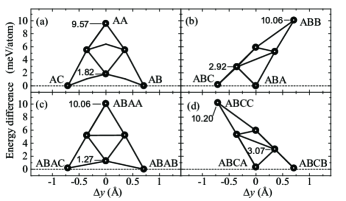
Figure 2(a) shows the calculated total energies of AX-bilayer graphite with different stacking configurations compared to that of the Bernal AB-bilayer, in which the translation of the top layer X is B (and equivalently C). The interlayer separation (to be referred to as ) has been optimized for each structures. Note that energies are represented in meV per carbon atom on the top overlayer, which in fact correspond to the exfoliation energies[12]. We see that AA structure marks, as is well-known, the highest energy of about 10 meV/atom with Å compared to the lowest energy of AB (AC) structure with Å. This energy of AA-bilayer is as large as a half of the exfoliation energy observed (22.8 meV/atom) or predicted (24 meV/atom) for graphite[12]. A translation of the top layer X from the in-plane position B to the nearest minimum C will encounter adiabatic energy barrier of 1.82 meV/atom at the midpoint, which is about 20 percent of the energy increase at the AA stacking.
This kind of barrier height is more pronounced (2.92 meV/atom) in ABX-trilayer graphite as shown in Fig. 2(b), in which the structure of the first two graphene layers are fixed at the AB-bilayer optimized by itself and the top layer is allowed to translate. The separations from the substrate AB-bilayer are optimized. ABC-trilayer with optimum separation of Å is found to have a slightly higher energy (0.18 meV/atom) than ABA with Å.
The behavior of barrier along the translational paths (Figs. 2(c) and (d)) is interesting in tetralayer graphite. The path linking ABAC (0.18 meV/atom) and ABAB (0 meV/atom by definition) has only a reduced barrier peak of 1.27 meV/atom, which would make transformation to Bernal stacking easier, whereas the path from ABCA (0.33 meV/atom) to ABCB (0.18 meV/atom) has a much harder barrier peak of 3.07 meV/atom. Since ABCB is equivalent to ABAC, we find that the most stable Bernal-type ABAB-tetralayer and the second most stable rhombohedral-type ABCA-tetralayer is separated by a translational barrier of about 3 meV/atom, if only a surface layer is allowed to move. These stable structures have a common optimum interlayer separation of Å. This result is consistent with the observation of rhombohedral structure in natural and synthesized graphite[12], and possibility of fabricating non-Bernal tri- and tetra-layer graphene films can be speculated. We have examined the effect of external electronic field on the relaxed structures of these FLGs. However, no discernible change in the order of stability and interlayer separations was found.
4 Band structures and field effect
For FLGs that have been found globally or locally minimum in total energy (i.e., AB-bilayer, ABA- and ABC-trilayer, and ABAB-, ABCA-, ABAC-, ABCB-tetralayer systems), we have calculated the band structures of the systems in the zero field and also in an uniform external electric field of strength mV/Å, applied perpendicular to the graphene plane. This field was represented by an additional sawtooth potential, which is piecewise proportional to with discontinuity at the mid-plane of the vacuum region in the cell. The potential difference applied between two adjacent graphene planes is Volts.
4.1 AB-bilayer graphite
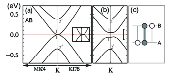
The band structure near the corner of BZ (K point) of AB-bilayer graphite with no external field is semi-metallic with chiral parabolic dispersions as shown in Fig. 3(a). The effect of perpendicular field opens an energy gap as shown in Fig. 3(b). The gap at the K point may indeed be understood in terms of the TB description (such as the SWMcC model[13]) of electrons as a lifted degeneracy of non-bonding orbitals, as a consequence of the effective field that breaks the symmetry along the -axis. The TB Hamiltonian of AB-bilayer graphite at the K point is identical to that for the system consists of one dimer and two equivalently isolated atoms as depicted in Fig. 3(c). Indices 1 and in Figs. 3(a) and (b) label monomeric non-bonding and dimeric bonding(antibonding) states at the K point. The hopping parameter for the dimer, which can be determined by a half the difference in eigenvalues of states at zero field, is found to be eV in agreement with the well-known value of the SWMcC model.
We point out that the gap at the K point, eV, is only 45 percent of the unscreened potential difference (indicated by the length of a bar in Fig. 3(c)) that the non-self-consistent TB model should predict. Our calculated result of the gap directly measures the effective field felt by the AB-bilayer film, and hence the dielectric response of bilayer graphite film against uniform and static perpendicular field, giving the dielectric constant of . This value of the internal effective field was also confirmed from the calculated lowest two eigenvalues of band at the BZ center( point).
In addition, no discernible influence of the field was found on the hopping parameter , because the field induced gap was perfectly consistent with that predicted by at zero field and effective potential difference , i.e., . Moreover, this fact was further confirmed in a separate calculation, in which the strength of the external field was doubled to widen the band gap at the K point to eV. Meanwhile, Ohta et al.[14] have reported significant change in the dimeric interaction with electron doping by potassium adsorption on a surface of AB-bilayer, from their angle-resolved photoemission experiments with analysis using TB fitting. This apparent contradiction with the present results might be related to the shift of Fermi level (electron number) due to doping in their system.
4.2 Trilayer graphite
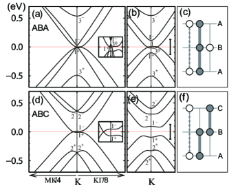
Figure 4(a) shows that the band structure near the corner of BZ (K point) of ABA-trilayer graphite film at zero field is semi-metallic with rather small overlap of conduction and valence bands. The TB Hamiltonian of the ABA-trilayer at the K point is equivalent to that for a linear trimer(see panel (c)) with hopping for the nearest neighbors and for the next neighbor that links both ends, and a perfectly non-bonding monomer, and a very weakly bonded (with ; a dashed link in panel (c)) dimer that opens a tiny gap (12 meV) between nearly -linear branches. This trimer at zero field has three states, which are to be referred to as bonding/antibonding and non-bonding states labeled by and , with eigenvalues and , respectively. Note that actually is the bonding state of orbitals at both ends via the second neighbor hopping .
On the other hand, ABC-trilayer graphite film at zero field is as shown in Fig. 4(d) a zero-gap semiconductor(or zero band-overlap semi-metal) with a band contact near the K point on the KM symmetry line. The gap at the K point is 20 meV, which arise from the splitting between bonding() and antibonding () states the weakly bonded dimer with the hopping parameter of meV. The strongly bonded dimers (Fig. 4(f)) are giving degenerate states.
The influence of the electric field on band structures of trilayer systems are shown in Fig. 4(d) and (e). We see the ABA-trilayer stays semi-metallic, because of the presence of almost degenerate states of non-bonding monomer in the middle plane (B) and trimer, which are nearly independent of the applied field. Whereas, the ABC-trilayer opens a energy gap at the K point, eV, and a minimum direct gap 0.146 eV. This energy gap is the – splitting and is nearly double the width of AB-bilayer’s induced by the same external field, reflecting the doubled thickness of the film, since the is order of magnitude smaller than the external potential difference. Therefore, the ABC-trilayer can be a tunable narrow-gap semiconductor if fabricated. The dielectric constant of ABA and ABC trilayers at the present applied field may be evaluated from the – splitting, which results in and .
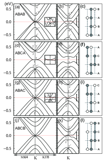
4.3 Tetralayer graphite
The band structures near the K point of four types of stable and metastable tetralayer graphite films are shown in Fig. 5. ABAC- and ACBC-stacked systems are obviously equivalent at zero electric field and even at an uniform field along c-axis they are equivalent when the reversed field is applied in either system. Therefore, the panel (k) may be thought of as the counterpart of panel (h) with reversed field.
The Bernal-type, ABAB-tetralayer system at the K point is equivalent to a linear tetramer and two weakly bonded dimers configured as is shown in panel (c). This clearly explains the distribution of Kohn-Sham eigenvalues at the K point in panel (a). The labels refer to the full bonding and antibonding states, and are semi-bonding and antibonding states of the linear tetramer. The external field lifts the degeneracy of upper and lower dimers. However, this does not leads to a band gap as show in panel (b) at this level of the field strength. From the splitting of weakly bonded dimeric states, the dielectric constant in the system is evaluated to be , almost no change from the Bernal trilayer’s value.
Similarly to the trilayer case, the rhombohedral-type ABCA-tetralayer system develops a flat or rather concave band gap as an uniform field comes in as shown in panel (e). The energy splitting of nearly non-bonding states (labeled as 1) on the top and bottom layers is 0.263 eV, which corresponds to . The induced narrow band gap will be controlled using a variable field.
The ABAC- or ABCB-stacked system has a very narrow band gap structure as shown in panel (g), which is rather similar to the semi-metallic band of ABA-trilayer around the K point at zero field, except for an overlaying dimeric band. When an external field is applied parallel to or anti-parallel to c-axis, the system becomes semi-metallic as plotted in panels (h) and (k). The and states are always very close, nearly independent of the uniform field, since they feel nearly the same averaged external potential. The dielectric constant is evaluated to be and at the present finite field, where we notice very small asymmetry due to the broken symmetry of the stacking sequence along the c-axis.
5 Conclusions
We have examined the stability of FLGs and found that for any number of layers Bernal FLGs are the most stable, but rhombohedral-type tri- and tetra-layer graphite films are also predicted to be possible structures, which are stabilized by relatively high energy barrier. In the rhombohedral-type FLGs including AB-bilayer, variable band gap will be induced by the on-set of perpendicular electric field, and other FLGs will stay semi-metallic. (Quite recentry, a report on ab initio band structures of FLGs at zero field[15] came into our notice. We found that the present results at zero field is in fine agreement with their results.) Therefore, experimental challenges for the fabrication of these non-Bernal FLGs would be very interesting.
Acknowledgments
The authors thank the CPMD consortium for the code.
References
- [1] K. S. Novoselov, A. K. Geim, S. V. Morozov, D. Jiang, Y. Zhang, S. V. Dubonos, I. V. Grigorieva and A. A. Firsov, Science 306, 666 (2004).
- [2] Y. Zhang, Y.-W. Tan, H. L. Stormer and P. Kim, Nature 438, 201 (2005).
- [3] K. S. Novoselov, E. McCann, S. V. Morozov, V. I. Falko, M. I. Katsnelson, U. Zeitler, D. Jiang, F. Schedin and A. K. Geim, Nature Physics 2, 177 (2006).
- [4] Y. Zheng and T. Ando, Phys. Rev. B 65, 245420 (2002).
- [5] B. Partoens and F. M. Peeters, Phys. Rev. B 74, 075404 (2006).
- [6] C. L. Lu, C. P. Chang, Y. C. Huang, J. M. Lu, C. C. Hwang and M. F. Lin, J. Phys.: Condens. Matter 18, 5849 (2006).
- [7] A. G. Marinopoulos, L. Reining, A. Rubio and V. Olevano, Phys. Rev. B 69, 245419 (2004).
- [8] CPMD, version 3.9.2, Copyright IBM Corp 1990–2006, Copyright MPI für Festkörperforschung Stuttgart 1997–2001.
- [9] S. Goedecker, M. Teter and J. Hutter, Phys. Rev. B 54 1703 (1998).
- [10] H. J. Monkhorst and J. D. Pack, Phys. Rev. B 13, 5188 (1976).
- [11] L. A. Girifalco and M. Hodak, Pack, Phys. Rev. B 65, 125404 (2002).
- [12] M. C. Schabel and J. L. Martins, Phys. Rev. B 46, 7185 (1992) .
- [13] J.-C. Charlier, J.-P. Michenaud and X. Gonze, Phys. Rev. B 46, 4531 (1992) .
- [14] T. Ohta, A. Bostwick, T. Seyller, H. Horn and E. Rotenberg, Science 313, 951 (2006).
- [15] S. Latil and L. Henrard, Phys. Rev. Lett. 97, 036803 (2006).