Dissipative Quantum Hall Effect in Graphene near the Dirac Point
Abstract
We report on the unusual nature of state in the integer quantum Hall effect (QHE) in graphene and show that electron transport in this regime is dominated by counter-propagating edge states. Such states, intrinsic to massless Dirac quasiparticles, manifest themselves in a large longitudinal resistivity , in striking contrast to behavior in the standard QHE. The state in graphene is also predicted to exhibit pronounced fluctuations in and and a smeared zero Hall plateau in , in agreement with experiment. The existence of gapless edge states puts stringent constraints on possible theoretical models of the state.
Electronic properties of graphene has attracted significant interest, especially since an anomalous integer quantum Hall effect (QHE) was found in this material Novoselov05 ; Zhang05 . Graphene features QHE plateaus at half-integer values of Hall conductivity where the factor 4 takes into account double valley and double spin degeneracy. The “half-integer” QHE is now well understood as arising due to unusual charge carriers in graphene, which mimic massless relativistic Dirac particles Novoselov04 . Recent theoretical efforts have focused on the properties of spin- and valley-split QHE at low filling factors Abanin06a ; Fertig06 ; Nomura06 ; Alicea06 ; Goerbig06 ; Abanin06b and fractional QHE Apalkov06 . Novel states with dynamically generated exciton-like gap were conjectured near the Dirac point Gusynin94 ; Khveshchenko01 ; Gusynin06 ; Fuchs06 . Experiments in ultra-high magnetic fields Zhang06 have so far revealed only additional integer plateaus at , and , which were attributed to valley and spin splitting.
The most intriguing QHE state is arguably that observed at . Being intrinsically particle-hole symmetric, it has no analog in semiconductor-based QHE systems. Interestingly, while it exhibits a step-like feature in , the experimentally measured longitudinal and Hall resistance Zhang06 ( and ) display neither a clear quantized plateau nor a zero-resistance state, the hallmarks of the conventional QHE. This unusual behavior was attributed to sample inhomogeneity Zhang06 and remains unexplained. In this Letter, we show that such behavior near the Dirac point is in fact intrinsic to Dirac fermions in graphene and indicates an opening of a spin gap in the energy spectrum Abanin06a . The gap leads to counter-circulating edge states carrying opposite spin Abanin06a ; Fertig06 which result in interesting and rather bizarre properties of this QHE state. In particular, even in the complete absence of bulk conductivity, this state has a nonzero (i.e. the QHE state is dissipative) whereby can change its sign as a function of density without exhibiting a plateau.
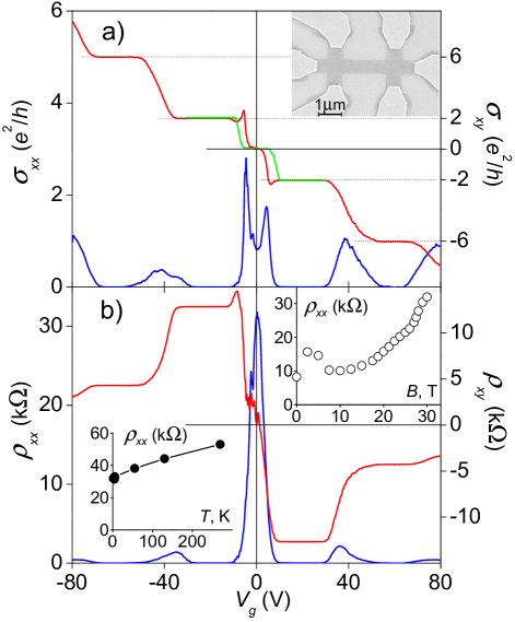
We start with reviewing the experimental situation near . Our graphene devices were fabricated as described in Ref.Novoselov04 and fully characterized in fields up to at temperatures down to . These measurements revealed the behavior characteristic of single-layer graphene Novoselov05 . Several devices were then investigated in up to , where, besides the standard half-integer QHE sequence, the plateau becomes clearly visible as an additional step in (Fig.1). We note, however, that the step is not completely flat, and there is no clear zero-resistance plateau in . Instead, exhibits a fluctuating feature away from zero which seems trying to develop in a plateau (Fig.1b). [In some devices passed through zero in a smooth way without fluctuations.] Moreover, does not exhibit a zero-resistance state either. Instead, it has a pronounced peak near zero which does not split in any field. The value at the peak grows from in zero ( for the shown devices) [1] to at (see inset of Fig.1b).
At this point, the absence of both hallmarks of the conventional QHE in these experiments can make one skeptical about the relation between the observed extra step in and an additional QHE plateau. However, the described high-field behavior near was found to be universal (reproducible for different samples, measurement geometries and magnetic fields above ). It is also in agreement with that reported in Ref.Zhang06 . Moreover, one can generally argue that the QHE at cannot possibly exhibit the usual hallmarks. Indeed, has to pass through zero because of the carrier-type change but cannot simultaneously exhibit a zero-resistance state because zero in both and would indicate a dissipationless (superconducting) state.
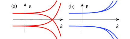
To explain the anomalous behavior of the high-field QHE (Fig.1), we note that all microscopic models near the Dirac point can be broadly classified in two groups, QH metal and QH insulator, as illustrated in Fig.2. Transport properties in these two cases are very different. The QH insulator (Fig.2b) is characterized by strongly temperature dependent resistivity diverging at low . The metallic -dependence observed at clearly rules out this scenario. In the QH metal (Fig.2a), a pair of gapless edge excitations (Fig.2a) provides dominant contribution to , while transport in the bulk is suppressed by an energy gap. Such dissipative QHE state will have , i.e. nominally small Hall angle and apparently no QHE. the roles of bulk and edge transport here effectively interchange: The longitudinal response is due to edge states, while the transverse response is determined mainly by the bulk properties.
From a general symmetry viewpoint advanced by Fu, Kane and Mele Liang06 the existence of counter-circulating gapless excitations is controled by invariants, protecting the spectrum from gap opening at branch crossing. In the spin-polarized QHE state Abanin06a this invariant is given by . While for other QHE states Gusynin94 ; Khveshchenko01 ; Gusynin06 ; Fuchs06 such invariants are not known, any viable theoretical model must present a mechanism to generate gapless edge states.
The metallic temperature dependence indicates strong dephasing that prevents onset of localization. To account for this observation, we suppose that the mean free path along the edge is sufficiently large, such that local equilibrium in the energy distribution is reached in between backscattering events. For that, the rate of inelastic processes must exceed the elastic backscattering rate: . This situation occurs naturally in the Zeeman-split QHE state Abanin06a , since backscattering between chiral modes carrying opposite spins is controlled by spin-orbital coupling which is small in graphene.
In the dephased regime, the chiral channels are described by local chemical potentials, , whose deviation from equilibrium is related to currents:
| (1) |
where is the total current on one edge. In the absence of backscattering between the channels the currents are conserved. In this case, since the potentials are constant along the edge, transport is locally nondissipative, similar to the usual QHE Halperin .
The origin of longitudinal resistance in this ideal case can be traced to the behavior in the contact regions. [Note the resemblance of each edge in Fig.3a with two-probe measurement geometry for the standard QHE.] We adopt the model of termal reservoirs Buttiker88 which assumes full mixing of electron spin states within Ohmic contacts (see Fig.3b). With currents , flowing into the contact, and equal currents flowing out, the potential of the probe is . Crucially, using Eq.(1), there is a potential drop across the contact,
| (2) |
equally for and . The voltage between two contacts positioned at the same edge (see Fig.3a) is equal to , which gives a universal resistance value Abanin06a . This is in contrast with the usual QHE where there is no voltage drop between adjacent potential probes Halperin ; Buttiker88 .
The longitudinal resistance increases and becomes nonuniversal in the presence of backscattering. It can be described by transport equations for charge density
| (3) | |||
| (4) |
where is the mean free path for 1d backscattering between modes and , and are compressibilities of the modes 1 and 2. In a stationary state, Eqs.(3) have an integral which expresses conservation of current . The general solution in the stationary current-carrying state is .
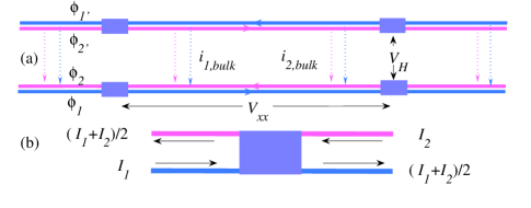
For the Hall bar geometry shown in Fig.3a, taking into account the contribution of voltage drop across contacts, Eq.(2), we find the voltage along the edge , where is the distance between the contacts. In the absence of transport through the bulk, if both edges carry the same current, the longitudinal resistance is
| (5) |
with the aspect ratio. From peak value (Fig.1) we estimate , which gives the backscattering mean free path of . The metallic -dependence of signals an increase of scattering with (Fig.1b inset). Similarly, growing with is explained by enhancement in scattering due to electron wavefunction pushed at high towards the disordered boundary.
An important consequence of the 1d edge transport is the enhancement of fluctuations caused by position dependence of the scattering rate . Solving for the potentials at the edge,
| (6) |
we see that the fluctuations in the longitudinal resistance scale as a square-root of separation between the contacts:
where is a microscopic parameter which depends on the details of spatial correlation of . Similar effect leads to fluctuations of the Hall voltage which has zero average value at . Assuming that the fluctuations of the potential at each edge, described by Eq.(6), are independent, we estimate , where is the bar length.
These fluctuations manifest themselves in noisy features in the transport coefficients near , arising from the dependence of the effective scattering potential on electron density. Such features can indeed be seen in and around (Fig.1b). As discussed below, away from bulk transport becomes important and short-circuits the edge. This will lead to suppression of fluctuations in and away from , in agreement with the behavior of the fluctuations in Fig.1b.
Another source of asymmetry in voltage distribution on opposite sides of the Hall bar is the potential drop on a contact, Eq. (2). This quantity can be nonuniversal for imperfect contacts, leading to finite transverse voltage. Such an effect can be seen in data in Fig.1 near , where Hall effect in a pristine system would vanish.
To describe transport properties at finite densities around , we must account for transport in the bulk. This can be achieved by incorporating in Eq.(3) the terms describing the edge-to-bulk leakage:
| (7) | |||
| (8) |
where are the up- and down-spin electrochemical potentials in the bulk near the boundary. Transport in the interior of the bar is described by tensor current-field relations with the longitudinal and Hall conductivities , for each spin component. Combined with current continuity, these relations yield the 2d Laplace’s equation for the quantities , with boundary conditions supplied by current continuity at the boundary:
| (9) |
where is a unit normal vector. [In Eq.(9) and below we use the units of .] To describe dc current, we seek a solution of Eqs.(7) on both edges of the bar with linear dependence which satisfies boundary conditions (9), where the functions have a similar linear dependence. The current is calculated from this solution as a sum of the contributions from the bulk and both edges. After elementary but somewhat tedious algebra we obtain a relation , where
| (10) |
with the bar width and . The quantities represent the sum of the bulk and edge contributions to Hall conductivities, and are defined as . The quantity , Eq.(10), replaces in Eq.(5). At vanishing bulk conductivity, , we recover .
The Hall voltage can be calculated from this solution as , where are variables at opposite edges. We obtain , where
| (11) |
This quantity vanishes at , since and at this point due to particle-hole symmetry.
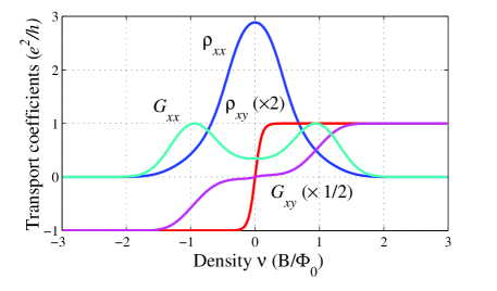
In Fig.4 we illustrate the behavior of the longitudinal and transverse resistance, calculated from Eqs.(10),(11) as
| (12) |
with , (the omitted contact term (2) is small for these parameters). Conductivities , are microscopic quantities, and their detailed dependence on the filling factor is beyond the scope of this paper. Here we model the conductivities by gaussians centered at , , as appropriate for valley-degenerate Landau level, whereby is related to by the semicircle relation semicircle_relation : . In Fig.4 we used , however we note that none of the qualitative features depend on the details of the model.
Fig.4 reproduces many of the key features of the data shown in Fig.1. The large peak in is due to edge transport near . The peak is reduced at finite because the edge is short-circuited by the bulk conductivity. The latter corresponds to the double peak structure in in Fig.4. We note that the part of between the peaks exceeds the superposition of two Gaussians which represent the bulk conductivity in our model. This excess in is the signature of the edge contribution. The transverse resistance is nonzero due to imbalance in for opposite spin polarizations away from the particle-hole symmetry point . Notably, does not show any plateau in the theoretical curve (Fig.4), while calculated from and exhibits a plateau-like feature. This behavior is in agreement with experiment (Fig.1 and Ref.Zhang06 ).
To conclude, QH transport in graphene at is due to counter-circulating edge states. In this dissipative QHE the roles of the bulk and the edge interchange: the edge states dominate in the longitudinal conductance, while the bulk conductivity determines the Hall effect. This model explains the observed behavior of transport coefficients, in particular the peak in and its field and temperature dependence, lending strong support to the chiral spin-polarized edge picture of the state.
This work is supported by EPSRC (UK), NSF MRSEC Program (DMR 02132802), NSF-NIRT DMR-0304019 (DA, LL), and NSF grant DMR-0517222 (PAL).
References
- (1) K. S. Novoselov, A. K. Geim, S. V. Morozov, D. Jiang, M. I. Katsnelson, I. V. Grigorieva, S. V. Dubonos, A. A. Firsov, Nature 438, 197 (2005);
- (2) Y. Zhang, Y.-W. Tan, H. L. Stormer and P. Kim, Nature 438, 201 (2005).
- (3) K. S. Novoselov, A. K. Geim, S. V. Morozov, D. Jiang, Y. Zhang, S. V. Dubonos, I. V. Grigorieva, and A. A. Firsov, Science, 306, 666 (2004); Proc. Natl. Acad. Sci. USA, 102, 10451 (2005).
- (4) D. A. Abanin, P. A. Lee and L. S. Levitov, Phys. Rev. Lett. 96, 176803 (2006).
- (5) H. A. Fertig and L. Brey, Phys. Rev. Lett. 97, 116805 (2006).
- (6) K. Nomura and A. H. MacDonald, Phys. Rev. Lett. 96, 256602 (2006)
- (7) J. Alicea and M. P. A. Fisher, Phys. Rev. B 74, 075422 (2006)
- (8) M. O. Goerbig, R. Moessner, B. Doucot, Phys. Rev. B74 161407 (2006)
- (9) D. A. Abanin, P. A. Lee, L. S. Levitov, cond-mat/0611062, unpublished.
- (10) V. M. Apalkov, T. Chakraborty, Phys. Rev. Lett. 97, 126801 (2006).
- (11) V. P. Gusynin, V. A. Miransky, and I. A. Shovkovy, Phys. Rev. Lett. 73, 3499 (1994).
- (12) D. V. Khveshchenko, Phys. Rev. Lett. 87, 206401 (2001) ibid. 87, 246802 (2001).
- (13) V. P. Gusynin, V. A. Miransky, S. G. Sharapov, I. A. Shovkovy, Phys. Rev. B74, 195429 (2006).
- (14) J.-N. Fuchs and P. Lederer, Phys. Rev. Lett. 98, 016803 (2007).
- (15) Y. Zhang, Z. Jiang, J. P. Small, M. S. Purewal, Y. W. Tan, M. Fazlollahi, J. D. Chudow, J. A. Jaszaczak, H. L. Stormer, and P. Kim, Phys. Rev. Lett., 96, 136806 (2006).
- (16) L. Fu, C. L. Kane, cond-mat/0606336; C. L. Kane and E. J. Mele, Phys. Rev. Lett. 95, 226801 (2005).
- (17) B. I. Halperin, Phys. Rev. B25, 2185 (1982).
- (18) M. Büttiker, Phys. Rev. B38, 9375 (1988).
- (19) A. M. Dykhne and I. M. Ruzin, Phys. Rev. B50, 2369 (1994); S. S. Murzin, M. Weiss, A. G. Jansen, and K. Eberl, Phys. Rev. B66, 233314 (2002)