Control of magnetic anisotropy in (Ga,Mn)As by lithography-induced strain relaxation
Abstract
We obtain control of magnetic anisotropy in epitaxial (Ga,Mn)As by anisotropic strain relaxation in patterned structures. The strain in the structures is characterized using sophisticated X-ray techniques. The magnetic anisotropy before patterning of the layer, which shows biaxial easy axes along [100] and [010], is replaced by a hard axis in the direction of large elastic strain relaxation and a uniaxial easy axis in the direction where pseudomorphic conditions are retained. This strong anisotropy can not be explained by shape anisotropy and is attributed solely to lattice strain relaxation. Upon increasing the uniaxial strain anisotropy in the (Ga,Mn)As stripes, we also observe an increase in magnetic anisotropy.
pacs:
75.50.Pp, 75.30.GwThe (Ga,Mn)As material system has been the focus of many studies over the last years. As the understanding of its complex transport and magnetic properties increases, the focus of interest shifts from basic research towards its application in devices. For this, it is necessary to understand how different parameters influence the ferromagnetic material in structures at the device level. In this letter we present a systematic study of the role of strain relaxation as the dominating factor contributing to the magnetic anisotropy in (Ga,Mn)As nanostructures. A (Ga,Mn)As layer grown epitaxially on a GaAs substrate is subject to compressive strain in the plane of the sample and typically exhibits biaxial in-plane easy axes along [100] and [010], at temperatures around 4 K Sawicki ; Wang . In earlier studies, control of the magnetic anisotropy has been achieved by modifying the strain in the layer. Tensile strain can be imposed on the (Ga,Mn)As by growing it on a thick, plastically relaxed (In,Ga)As buffer with a larger lattice parameter, and results in an out-of-plane easy axis Liu ; Xiang .
Here, we follow an alternative approach in modifying the lattice strain of (Ga,Mn)As on GaAs by lithography, which allows us to locally control the magnetic anisotropy of the material. By structuring a fully pseudomorphic 70 nm (Ga,Mn)As layer into thin, elongated stripes, we allow anisotropic, elastic strain relaxation perpendicular to the long axis of the stripe. To increase the strain in the structure compared to the case of (Ga,Mn)As on GaAs, a second sample is processed which includes a highly compressively strained layer acting as an extra stressor to the overlying (Ga,Mn)As layer. The uniaxial strain relaxation in the structures is investigated by grazing incidence X-ray diffraction (GIXRD) and high-resolution X-ray diffraction (HRXRD). To determine the influence of patterning on the magnetic anisotropy, a series of magnetometric and magnetotransport studies are performed. We also present finite-element simulations of anisotropic strain relaxation and kp calculations which confirm the relationship between the structural and magnetic behavior observed in our samples.
The samples are grown in a dedicated III-V MBE chamber with effusion cells for Ga, In, Mn, and a valved As4 cell. A 200 nm thick high-quality GaAs buffer is deposited at ∘C, on an epi-ready semi-insulating (001) GaAs substrate, to improve surface and layer quality. During a growth interruption, the temperature is reduced to 270 ∘C. At this temperature, a (Ga,Mn)As layer of 70 nm thickness is deposited at a rate of 0.86 Å/s and a beam equivalent pressure of As4/Ga = 25. The Mn content is determined by HRXRD to be % Schott . For one sample an additional 80 nm thick (In,Ga)As layer with 7.4% In was grown at 500 ∘C prior to (Ga,Mn)As deposition.
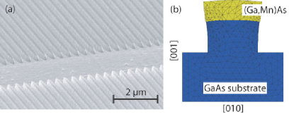
After growth, electron beam lithography and chemically assisted ion beam etching are used to pattern both samples into the structure shown in Fig. 1a. A total area of 4 x 4 mm is covered by arrays of stripes, each individual stripe measuring nominally 200 nm x 100 m with a separating distance of 200 nm. The etch depth is about 200 nm, thus well into the GaAs buffer layer. The stripes are aligned along the [100] crystal direction.
To optimize the stripe dimensions, the relaxation of the stripes has been modeled by finite element simulations prior to sample preparation. The simulation makes use of elasticity theory to describe the strain and displacements in the stripe structure by minimizing strain energy. A typical resulting cross-section of a stripe after relaxation is displayed in Fig. 1b. Simulations for varied stripe dimensions at a fixed material composition suggest that a spatially rather homogeneous elastic relaxation of the (Ga,Mn)As stripe core is reached for stripe widths below about 500 nm, while inhomogeneous strain relaxation, concentrated primarily at the edges of the stripe, is observed for wider structures. The etch depth also plays a critical role in degree and homogeneity of strain relaxation. As the substrate pillar height is reduced, the relaxing layer is more restricted at the lower interface resulting in reduced relaxation and a strain gradient along the [001] direction.
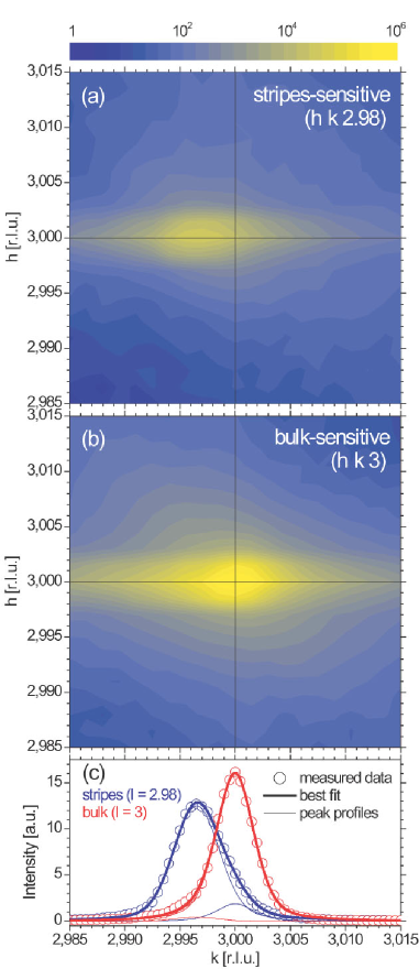
The strain relaxation in the (Ga,Mn)As stripes is determined from GIXRD reciprocal space mapping in the vicinity of the (333) Bragg reflection. The GIXRD experiments were performed at beamline BW2 of the Hamburger Synchrotronstrahlungslabor (HASYLAB). Due to the small lattice mismatch between GaAs and (Ga,Mn)As of , the Bragg reflections of both materials lie very close to each other. If the (Ga,Mn)As stripes were purely pseudomorphically strained, the difference between both reflections would be only r.l.u. (reciprocal lattice units), a value which can hardly be resolved with our experimental setup. However, since the thickness of the layer is only about 70 nm, the (Ga,Mn)As (333) reflection is significantly broadened in -direction. Therefore, by mapping the reciprocal space close to but not precisely at the -position of the GaAs bulk-peak one is mainly sensitive to the (Ga,Mn)As stripes. This measurement, a --map at , is shown in Fig. 2a, and a similar map through the GaAs bulk-peak in Fig. 2b. The latter is a bulk-sensitive measurement and shows a peak located at (333) providing a coordinate system of the lattice units. In the stripes-sensitive measurement, one can clearly observe (Fig. 2a) a shift of the peak towards smaller values in . This shift indicates the relaxation of the (Ga,Mn)As structure in [010] direction, whereas in [100] direction no relaxation takes place (no peak shift visible in -direction). The different widths of the peaks in - and -direction are due to the different lateral dimensions of the stripes.
In order to quantify the shift, we fit the measured peaks to Voigt-profiles. Fig. 2c shows the central line scan through the peaks of both reciprocal space maps (open circles in the figure). Each curve is fit with the sum of two Voigt-peaks (thick solid lines), one fixed at representing the bulk-contribution, the other with a variable position. All four individual peaks are also shown as thin lines. By this procedure we obtain a value for the strain in [010] direction of /. We conclude that the (Ga,Mn)As stripes are pseudomorphically strained in the [100]- but show a large degree of strain relaxation in the [010]-direction.
For magnetic characterization, a superconducting quantum interference device (SQUID) is used to measure magnetization behavior along selected directions in the parent and patterned layers. The results are shown in Fig. 3.
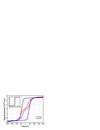
The parent layer (inset of Fig. 3) exhibits the well known biaxial anisotropy at 4 K with easy axes along the [100] and [010] crystal directions and hard axes along [10] and [110]. The two easy axes are both plotted but not distinguishable in the inset. Fig. 3 shows the anisotropy after patterning. Along the [010] direction, the magnetic moment at zero field drops by % compared to the [100] direction. This previously easy axis is now clearly a very hard magnetization axis. The remaining easy axis along [100] also reflects this change by an increase in coercive field from 4 mT in the parent layer to 43 mT in the patterned layer. This effect is caused by the increased energy necessary to rotate the magnetization through the now hard [010] axis during magnetization reversal. Thus, the presented results show a clear modification of the magnetic anisotropy of nanopatterned (Ga,Mn)As/GaAs stripes.
The observed strong anisotropy can not be explained by shape anisotropy. As-grown (Ga,Mn)As shows mainly biaxial crystalline magnetic anisotropy ( J/m3), which dominates the magnetic reversal behavior. Calculating the uniaxial term stemming from the shape anisotropy produced by our geometry (ferromagnetic prism Aharoni ) leads to J/m3, much smaller than the crystalline anisotropy contribution. Thus we attribute the observed emergence of the dominant uniaxial anisotropy in our samples to the anisotropic strain relaxation which, as we show in the kp modeling below, contributes an additional term in the magnetostatics energy equation, with enough impact to overcome the otherwise dominant biaxial anisotropy.
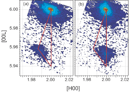
It is possible to further increase the strength of the imposed uniaxial anisotropy by increasing the strain in the parent layer. For this we use an (In,Ga)As layer with considerably larger lattice mismatch of to the substrate, deposited prior to the (Ga,Mn)As layer with . This layer, which is grown to a thickness close to but below the critical value for plastic strain relaxation, acts as a stressor to the overlying (Ga,Mn)As layer. In Fig. 4 we present HRXRD data of the patterned stripe structure. To distinguish between the lattice constants along the long axis of the stripes ([100] direction) and perpendicular to the stripes ([010] direction), two reciprocal space maps (RSM) of the (206) Bragg reflection were taken with the incident X-ray beam perpendicular (Fig. 4a) and parallel (Fig. 4b) to the stripe axis. In the first case, the (In,Ga)As layer peak maximum clearly indicates a larger lateral and smaller vertical lattice constant than expected for a fully pseudomorphic layer (bottom tip of the relaxation triangle). The (Ga,Mn)As layer is expected to have a similar lateral lattice constant and therefore lateral peak coordinate in the RSM to the underlying (In,Ga)As. Hence, the bulge in the substrate peak at (1.992, 5.988) and (2.000, 5.986) in Fig. 4a and Fig. 4b, respectively, is attributed to the (Ga,Mn)As layer. Because of the peak location, we conclude that tensile strain () has been induced by the relaxed (In,Ga)As layer. With incident X-rays along [100] (Fig. 4b), both layer peaks are located directly below the substrate peak, but shifted to smaller vertical lattice constant (due to Poisson effect) compared to the biaxial pseudomorphic case. The position of the peaks in both maps can be explained unambiguously by a large uniaxial strain relaxation in the [010] crystal direction while retaining fully pseudomorphic conditions along the [100] direction.
This sample shows a very similar behavior in SQUID compared to the pure (Ga,Mn)As sample, with the well-known biaxial easy-axes in the parent layer, as well as the emergence of the strong uniaxial anisotropy after patterning.
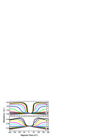
That the imposed uniaxial anisotropy in the sample containing the (In,Ga)As layer stressor is even stronger, can be inferred from magnetoresistance measurements. In (Ga,Mn)As, which is inherently highly p-doped by Mn, a strong anisotropic magnetoresistance (AMR) is generally observed. The magnetoresistance is dependent on the angle between the magnetization and the current McGuire , with a minimum when is parallel to the current Baxter . For the measurement (see Fig. 5), about 250 parallel stripes are contacted from both ends. A series of magnetic field sweeps from T to 0.3 T is performed, with incremental increase of the angle between and after each sweep. In both samples, all (hysteretically symmetric) curves share one low resistance state at T. When the field sweep is performed in the [100] direction (), the resistance remains at the low state. With increasing angle between and , a high resistance state develops and reaches a maximum at . At this angle, the magnetization starts out parallel to the stripes (low resistance) and is forced to the unfavorable direction perpendicular to the stripes (high resistance) at high fields. As with the SQUID results, these findings fit perfectly into the picture of a strain induced uniaxial magnetic anisotropy. We also observe a larger opening of the curves from the additionally strained stripes (lower part of Fig. 5). This is a direct evidence of an increased anisotropy field, as more energy is necessary to rotate the magnetization into the unfavorable hard [010] direction. According to nanobars , we determine the magnitude of the anisotropy field from these openings to be mT for the pure (Ga,Mn)As stripes and mT for the additionally strained stripes. As the strain in the magnetic layer of the second sample is demonstrably significantly different with nominally identical physical dimensions, this effect can clearly be attributed to the lattice strain, considering that shape anisotropy is identical for both structures.
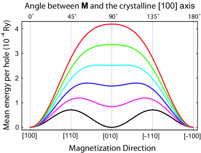
Finally, we present the results of kp calculations Dietl of the magnetization-direction dependence of the mean energy per hole. The results support our interpretation that strain is the key element in determining the magnetic anisotropy in (Ga,Mn)As nanostructures. Fig. 6 shows the evolution of the equivalent energy minima along [100] and [010] for fully biaxially strained (Ga,Mn)As (black curve) with increasing degree of strain relaxation in the [010] direction. Assuming homogeneous strain distribution in the stripes and a moderate carrier density cm-3, we can deduce from the calculations, that the uniaxial contribution from strain dominates over the biaxial term to such a degree, that above only a single stable point, along [100], remains. This is characteristic of perfect uniaxial behavior. As we demonstrated above in connection with the X-ray data, our patterned samples exhibit strain levels that exceed this number. The difference by a factor of 2 in the anisotropy fields for the two differently strained samples (Fig. 5) also agrees well with the model prediction (we find a factor of 3). We conclude that our experiments and modeling unambiguously demonstrate that lithographic pattering, when necessary combined with the (In,Ga)As stressor technique, is a reliable and versatile tool for controlling the magnetic anisotropies in (Ga,Mn)As. We anticipate that this local technique should prove very useful for device applications.
We thank T. Borzenko, A. Stahl, I. Gierz, and E. Umbach as well as the staff at HASYLAB for their help in this work. We acknowledge financial support from the DFG (BR 1960/2-2 and SFB 410) and the EU (NANOSPIN FP6-IST-015728 and the IHP programme “Access to Research Infrastructures“).
References
- (1) M. Sawicki, F. Matsukura, A. Idziaszek, T. Dietl, G.M. Schott, C. Ruester, C. Gould, G. Karczewski, G. Schmidt, and L. W. Molenkamp, Phys. Rev. B 70, 245325 (2004)
- (2) K. Y. Wang, M. Sawicki, K. W. Edmonds, R. P. Campion, S. Maat, C. T. Foxon, B. L. Gallagher, and T. Dietl, Phys. Rev. Lett. 95, 217204 (2005)
- (3) X. Liu, W. L. Lim, L. V. Titova, M. Dobrowolska, J. K. Furdyna, M. Kutrowski, T. Wojtowicz, J. Appl. Phys. 98, 63904 (2006)
- (4) G. Xiang, A. W. Holleitner, B. L. Sheu, F. M. Mendoza O. Maksimov, M. B. Stone, P. Schiffer, D. D. Awschalom, N. Samarth, Phys. Rev. B 71, 241307 (2005)
- (5) G. M. Schott, G. Schmidt, L.W. Molenkamp, R. Jakiela, A. Barcz, and G. Karczewski, Appl. Phys. Lett. 82, 4678 (2003)
- (6) D. V. Baxter, D. Ruzmetov, J. Scherschligt, Y. Sasaki, X. Liu, J. K. Furdyna, C. H. Mielke, Phys. Rev. B 65, 212407 (2002)
- (7) a) T. R. McGuire, R. I. Potter, IEEE Trans. Magn. 1975, MAG-11, 1018. b) J. P. Jan, in Solid State Physics (Eds: F. Seitz, D. Turnbull), Academic Press Inc., New York, 1957
- (8) A. Aharoni, J. Appl. Phys. 83, 3432 (1998)
- (9) S. Hümpfner, M. Sawicki, K. Pappert, J. Wenisch, K. Brunner, C. Gould, G. Schmidt, T. Dietl and L.W. Molenkamp, submitted, and cond-mat/0612439
- (10) T. Dietl, H. Ohno, and F. Matsukura, Phys. Rev. B 63, 195205 (2001)