Exploiting Locally Imposed Anisotropies in (Ga,Mn)As: a Non-volatile Memory Device
Abstract
Progress in (Ga,Mn)As lithography has recently allowed us to realize structures where unique magnetic anisotropy properties can be imposed locally in various regions of a given device. We make use of this technology to fabricate a device in which we study transport through a constriction separating two regions whose magnetization direction differs by . We find that the resistance of the constriction depends on the flow of the magnetic field lines in the constriction region and demonstrate that such a structure constitutes a non-volatile memory device.
(Ga,Mn)As can be regarded as a prototypical material for investigating potential device applications of ferromagnetic semiconductors. The spin-orbit mediated coupling of magnetic and semiconductor properties in this material gives rise to many novel transport-related phenomena which can be harnessed for device applications. Previously reported device concepts include strong anisotropic magnetoresistance (AMR), in-plane Hall effect Roukes , tunneling anisotropic magnetoresistance (TAMR) GouldTAMR ; ChrisTAMR ; KatrinTAMR and Coulomb blockade AMRCBAMR . These previous demonstrations have been based on structures which have the same magnetic properties, inherited from the unstructured (Ga,Mn)As layer, throughout the device. Improvement in lithographic capabilities nanobars has recently allowed for the first time the production of structures where distinct anisotropies are imposed locally to various functional elements of the same device by overwriting the parent layer anisotropy. This greatly enhances the scope of possible device paradigms open to investigation as it allows for devices where the functional element involves transport between regions with different magnetic anisotropy properties.
In this letter we present the first such device. It is comprised of two (Ga,Mn)As nanobars, oriented perpendicular to each other, and with each nanobar exhibiting strong uniaxial magnetic anisotropy. These two nanobars are electrically connected through a constriction whose resistance is determined by the relative magnetization states of the nanobars. We show that the anisotropic magnetoresistance effect yields different constriction resistances depending on the relative orientation of the two nanobar-magnetization vectors. The structure can thus be viewed as the basis of a ferromagnetic semiconductor memory device that operates in the non-volatile regime.
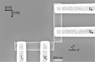
For the device, we use a 20 nm thick (Ga,Mn)As layer grown on a GaAs substrate growth by low-temperature molecular beam epitaxy. Using an electron-beam lithography(EBL) defined Ti-mask and chemically assisted ion beam etching (CAIBE) this layer is patterned into several pairs of coupled nanobarsnanobars as shown in the SEM micrograph in Fig. 1. Ti/Au contacts are defined in another EBL-step through metal evaporation and lift-off, yielding resistance area products of cm2. The bars are circa 200 nm wide and 1m long and oriented along the [100] and [010] crystal direction, respectively. They form a -angle and touch each other in one corner, where a constriction with a width of some tens of nm is formed.
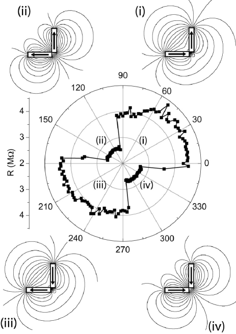
Transport measurements are carried out at 4 K in a magnetocryostat fitted with a vector field magnet that allows the application of a magnetic field of up to 300 mT in any direction. The sample state is first ”written” by an in-plane magnetic field of 300 mT along a writing angle (as defined in Fig. 1). The field is then slowly swept back to zero while ensuring that the magnetic field vector never deviates from the -direction. We measure the four-terminal resistance of the constriction in the resulting remanent state by applying a voltage to the current leads ( and ), and recording both the voltage drop between contacts and and the current that is flowing from to (Fig. 1). The polar plot of Fig. 2 shows the constriction resistance of the remanent magnetization state as a function of the writing angle . The resistance, which is dominated by the constriction, has a higher value upon writing the sample in the (extended) first quadrant () and a lower value upon writing in the (shrunken) second quadrant (). As a whole the plot is point-symmetric with respect to the origin.
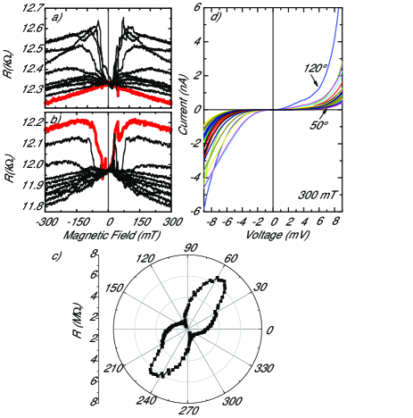
To explain these results, we first examine the behavior of the individual nanobars. They are patterned on the sub-micron scale to make use of anisotropic strain relaxation, which in turn causes a uniaxial magnetic anisotropy that is strong enough to overwrite the intrinsic anisotropy of the (Ga,Mn)As layernanobars . We therefore expect each nanobar to show a uniaxial magnetic anisotropy with a magnetic easy axis along the respective long axis of each of the nanobars. That this is true also for coupled nanobars is confirmed in Fig. 3, which shows two terminal magnetoresistance scans, performed separately on the -nanobar (Fig. 3a) and the -nanobar (Fig. 3b) pictured in Fig. 1. The plots show field sweeps from -300 to +300 mT for various in-plane field directions between and . Metallic (Ga,Mn)As exhibits a higher resistance value when the magnetization M is perpendicular to the current J, than when M is parallel to J (this is the AMR effect Jan ,AMRGaMnAs ). When the field H is swept along (thick line in Fig. 3a), the resistance of the -nanobar remains in the low state NOTE , indicating that M is parallel to J throughout the entire magnetic field range. All the other MR-scans start at a higher resistance value and merge into the low resistance curve at zero field, indicating that M, which is almost parallel to H at high fields, relaxes towards the uniaxial easy axis as the field is decreased. Analogously, the uniaxial easy axis of the -nanobar is along (Fig. 3b). Consequently, the -MR-scan is a flat low resistance curve. During the -scan (thick line) the magnetization relaxes from parallel to the field (high resistance) towards the easy axis along the bar (low resistance) at zero field.
Given that both bars show a uniaxial magnetic easy axis along their respective long axis, the structure has four possible magnetic states at zero magnetic field as sketched in Fig. 2. In sectors (i) and (iii) the nanobars are magnetized ”in series”,i.e. the magnetization vectors meet in a configuration which we will call head-to-tail. In (ii) and (iv) on the other hand, both magnetization vectors point away from (tail-to-tail) or towards (head-to-head) the constriction. When the sample is magnetized along a given direction at 300 mT, the magnetization of both bars is almost parallel to the magnetic field. As the field is then lowered to zero, the magnetization of each nanobar relaxes to the respective nanobar easy axis, selecting the direction which is closest to the writing angle . For a nanobar along this means, assuming no interaction between the bars, that M relaxes to upon writing the bar along any angle between and ; otherwise M relaxes to . If the bars in our device were non-interacting, one would thus expect the magnetization configuration in each quadrant to be as depicted in the sketches of Fig. 2, with each quadrant accounting for exactly one fourth of the total plot.
The deviation from this behavior in the actual device is due to magnetostatic interactions between the two bars, which cause a preference for head-to-tail configurations. A simple magnetostatic calculation shows that the repulsive field felt by the tip of one bar due to being near the wrong pole of the other bar is of the order of 2 mT, which is of the uniaxial anisotropy field. The energy density of this field is thus strong enough to overcome a small part of the energy barrier against rotation towards the opposite magnetization direction, which corresponds to an angle of . The head-to-tail quadrants thus increase commensurably.
Magnetic field line patterns for the four magnetization configurations were calculated (sketches in Fig. 2i-iv) using a simple bar magnet model. The field lines are close to parallel to the current in the head-to-tail configuration (Fig. 2i and iii). In the tail-to-tail and the head-to-head configuration (Fig. 2ii and iv) the field lines are approximately perpendicular to the current.
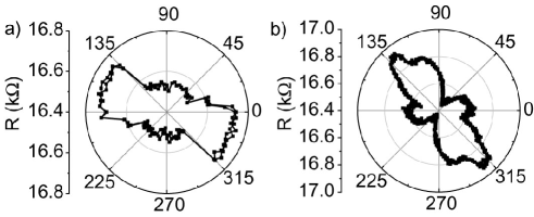
Having understood the magnetic configuration of the device in the write-read experiment of Fig. 2, we now turn to an explanation of why these should lead to two very distinct resistance states. The above magnetostatic arguments and internal fields, in connection with the AMR coefficient for metallic (Ga,Mn)As can explain a few percent resistance difference AMRGaMnAs ; Roukes between the head-to-tail and the head-to-head configuration, much smaller and of a different sign than the effect in Fig. 2. We have actually observed such a small AMR related effect in a similar structure, which has a wider constriction (100 times lower constriction resistance). Fig. 4a shows similar data on this low resistance sample as Fig. 2 for the high resistance sample. It is immediately obvious from Fig. 4a that this sample shows the same remanent magnetization configurations as the device in Fig. 2. However, the effect is much smaller and of the opposite sign: where Fig. 2 exhibits a high resistance state, Fig. 4a shows a low state, and vice versa.
We ascribe the difference in behavior between Figs. 2a and 4a to the occurrence of depletion in the constriction in the sample of Fig. 2a, which drives the transport (in the critical constriction region) into the hopping regimeChrisNanoconstr . At the same time, we suggest that in the hopping regime the AMR coefficient changes sign, leading to the observed changes in magnetoresistance. Important evidence for this claim comes from the angle-dependent magnetoresistance behavior of the samples at a field of 300 mT, strong enough to force the magnetization close to parallel to the external field. This data is given in Fig. 3c for the high-resistance, and in Fig. 4b for the low-resistance sample.
The low-resistance device exhibits typical AMR behavior as expected for metallic (Ga,Mn)As: Fig. 4b shows that the resistance is lowest when M is forced parallel to the current through the constriction () and ca. 3 % higher for MJ. In contrast, the high-resistance constriction of the device in Fig. 2 shows a huge and inverted AMR signal, as can be seen in Fig. 3c. The resistance at , where MJ, is more than 5 times larger than for MJ.
This is actually not the first observation of an inverted AMR signal; the same effect has recently been reported in thin (Ga,Mn)As devices CBAMR ; Andrew in which the transport is in the hopping regime. This situation is similar to our high-resistance device, where from the resistance one already can infer that the constriction acts as a tunnel barrier. Actual evidence for tunneling transport comes from the current-voltage characteristics of the high-resistance constriction, shown in Fig. 3d, which were taken at 300 mT at different field directions . The I-V’s are clearly non-linear, with the nonlinearity depending on the magnetization direction. Fields aligning M along cause the strongest and along the smallest non-linearity of the IV-curve.
The strong dependence of the IV-characteristic and the resistance on the magnetization direction are characteristic of transport going through a metal-insulator transition (MIT) from the diffusive into the hopping regime depending on the angle of the magnetization, similar to what we have previously observed in a TAMR device KatrinTAMR . Such a MIT occurs in partly depleted samples due to the wave-function geometry change depending on the magnetization direction. The localized hole wave-function has an oblate shape with the smaller axis pointing in the magnetization direction (wavefunction ). Consider the overlap of such oblate shapes statistically distributed with respect to the direction of the current in connection with the Thouless localization criterion. The wavefunction overlap is much smaller when the sample is magnetized parallel to the current, than for , suppressing hopping transport through the depleted constriction region. This implies a magnetoresistance behavior that is exactly the inverse of that expected for the metallic regime and explains the increased resistance value in both the high field measurements (Fig. 3c along ) and the write-read experiment (Fig. 2 1st quadrant).
We thus believe that our observations can be fully explained by the internal magnetic fields and the AMR coefficient as applicable to the transport regime in the constriction. A further candidate to explain our observations could be the presence of a domain wall (DW) between differently magnetized regions of the device in the head-to-head and tail-to-tail configuration, which would be absent in the head-to-tail configurations. However, since the constriction is long and the DW would not be strongly geometrically confined, one anticipates only a very low DW resistance in these samples ChrisNanoconstr ; Bruno . This is confirmed by a comparison of Fig. 2 with Fig. 3c: The resistance values of both remanent states in Fig. 2 are in between the extreme resistance values of the homogeneously magnetized sample. The DW contribution ChrisNanoconstr to the constriction resistance can in the present sample thus only be a minor effect on the resistance of the remanent state and does not explain the different resistance levels in Fig. 2. notegeorg . In the remanent state the resistance of the head-to-head configuration, including a possible DW contribution, is lower than the resistance of the head-to-tail configuration. We can thus exclude the DW as the origin of the two resistance states observed in Fig. 2.
In conclusion we have shown that locally imposed magnetic anisotropies in different regions of one ferromagnetic semiconductor device allow for novel device designs. We consider the perpendicularly magnetized nanobars discussed in this paper as a first demonstration of the type of devices that can be fabricated using this approach, it is certainly not difficult to conceive of further concepts in this direction. In addition, the work presented here has highlighted the difference in AMR behavior between metallic and hopping transport in (Ga,Mn)As, which again should prove useful in device design.
Acknowledgements.
The authors thank M. Sawicki and M.J. Schmidt for useful discussions and V. Hock and T. Borzenko for help in sample fabrication. We acknowledge financial support from the EU (NANOSPIN FP6-IST-015728) and the German DFG (BR1960/2-2).References
- (1) H. X. Tang, R.K. Kawakami, D.D. Awschalom and M.L. Roukes, Phys. Rev. Lett. 90, 107201 (2003).
- (2) C. Gould, C. Rüster, T. Jungwirth, E. Girgis, G.M. Schott, R. Giraud, K. Brunner, G. Schmidt, and L.W. Molenkamp, Phys. Rev. Lett. 93, 117203 (2004).
- (3) C. Rüster,C. Gould, T. Jungwirth, J. Sinova, G. M. Schott, R. Giraud, K. Brunner, G. Schmidt, and L. W. Molenkamp , Phys. Rev. Lett. 94, 027203 (2005).
- (4) K. Pappert, M. J. Schmidt, S. Hümpfner, C. R ster, G. M. Schott, K. Brunner, C. Gould, G. Schmidt, and L. W. Molenkamp, Phys. Rev. Lett. 97, 186402 (2006).
- (5) J. Wunderlich, T. Jungwirth, B. Kaestner, A. C. Irvine, A. B. Shick, N. Stone, K.-Y. Wang, U. Rana, A. D. Giddings, C. T. Foxon, R. P. Campion, D. A. Williams, and B. L. Gallagher, Phys. Rev. Lett., 97, 077201 (2006).
- (6) S. Hümpfner, M. Sawicki, K. Pappert, J. Wenisch, K. Brunner, C. Gould, G. Schmidt, T. Dietl and L.W. Molenkamp, submitted, and cond-mat/0612439
- (7) For details of the growth, see G.M. Schott, G. Schmidt, G. Karczewski, L.W. Molenkamp, R. Jakiela, A. Barcz, G. Karczewski, Appl. Phys. Lett., 82, 4678 (2003)
- (8) a) J. P. Jan, in ”Solid State Physics” (Eds: F. Seitz, D. Turnbull), Academic Press Inc., New York, 1957. b) T.R. McGuire, R.I. Potter, IEEE Trans. Magn. MAG-11, 1018 (1975).
- (9) D.V. Baxter, D. Ruzmetov, J. Scherschligt, Y. Sasaki, X. Liu, J.K. Furdyna, C.H. Mielke, Phys. Rev. B 65, 212407 (2002)
- (10) The remaining constant slope is caused by the isotropic MR effect as described, e.g., in F. Matsukura, M. Sawicki, T. Dietl, D. Chiba, H. Ohno, Physica E 21, 1032 (2004).
- (11) C. Rüster, T. Borzenko, C. Gould, G. Schmidt, L.W. Molenkamp, Phys. Rev. Lett. 91, 216602 (2003).
- (12) A.W.Rushforth, K.Vyborny, C.S.King, R.P.Campion, C.T. Foxon, T.Jungwirth and B.L.Gallagher, to be published
- (13) M.J. Schmidt,K. Pappert, C. Gould, G. Schmidt, R. Oppermann, and L.W. Molenkamp, to be published
- (14) P. Bruno, Phys. Rev. Lett. 83, 2425 (1999).
- (15) Field line patterns calculated using Vizimag (www.vizimag.com).
- (16) In a separate experiment we have prepared a DW pinned at the smallest part of our constriction. This was accomplished using well defined field sequences and will be published elsewhere. In this case we observe a large positive DW contribution to the device resistance (as reported in ChrisNanoconstr ).