Effective Mass Anomalies in Strained Si Thin Films and Crystals
Abstract
Effective mass anomalies due to the geometrical effects are investigated in silicon nanostructures using first-principles calculations for the first time. In {111} and {110} biaxially strained Si, it is found that longitudinal effective mass is extraordinarily enhanced for both thin films and crystals. This mass enhancement is caused by the change of the band structure with double minima into that with a single minimum due to strain and confinement. At the transition point, it is analytically shown that the effective mass diverges. The dependences of the confinement thickness on the anomalies are qualitatively explained by an extension of the effective mass approximation.
pacs:
73.22.-f,71.55.Cn,73.61.Cw,71.55.CnI
I.1
I.1.1
In this decade, various nanostructures have been fabricated and measured. In such small structures, the geometrical effect due to strain, confinement, and crystal directions significantly changes the electronic structures compared with that of the bulk. Intentional use of the geometrical effect has been suggested for the improvement of the device performanceTakagi96 . From the technological viewpoint, the function of sub-nm-body metal oxide field-effect transistors (MOSFETs) using silicon on insulatorSOI has been demonstrated, which consist of a silicon transport region sandwiched by insulating layersUchida03 . The nanostructure most sensitive to the geometrical effect may be an ultrathin body double-gate (UTBD) MOSFETBalestra87 ; Gamiz01 with a body thickness of less than 10nm; it has a three dimensional structure with the channel region sandwiched by two gate insulators and is a promising sub-10 nm device. Recently, in terms of electron mobility for the UTBD MOSFET, the advantage of the direction due to the valley structure has been reported in comparison with the directionTsutsui05 . It is very interesting to investigate the change of the electronic structures including transport parameters such as effective mass from the bulk to the thin films of some atomic layers. However, there are few studies on the intrinsic properties of semiconductor films in the intermediate region from the bulk to the sub-nm body using first-principles calculationsYamauchi05 .
In this Letter, the effective mass is systematically investigated for the biaxially strained Si thin films confined in the , , and directions and for strained Si crystals using density functional calculations, where the strain is uniformly applied to the plane perpendicular to the confinement direction. In the {111} and {110} strained Si, it is found that in some region, longitudinal effective mass is extraordinarily enhanced for the thin films and the crystals. Preliminary results are reported in Yamauchi07 . The confinement and the symmetry breaking due to the strain cause these anomalies, where the band structures change from double minima to a single minimum. In such a case, it is analytically shown that the effective mass diverges. As far as the author knows, this is the first report on the qualitative change of the band structure and the divergence of the effective mass in Si caused by confinement and strainRideau . The dependences of the confinement thickness on the anomalies are qualitatively explained by extending the effective mass approximation to the whole band near the Brillouin zone boundary. The experimentally observable regions of the strain and thickness are also obtained for the confinement.
Band calculation is based on the density functional theoryHohenberg64 ; Kohn65 . The local density approximation (LDA) PW92Perdew92 is adopted for the exchange correlation functional. To describe ion-electron interaction, norm-conservingTroullier90 and ultrasoftVanderbilt90 pseudopotentials are adopted for Si and Cl, and for H, respectively. The calculational condition is carefully checkedcalc-cond . The cutoff energy is 20.25 Rydberg. The meshes of the sampled k-points are , , and for the (001), (111) and (110) slabs, respectively. The calculated longitudinal and transverse masses for the bulk without strain are 0.950 (0.9163) and 0.189 (0.1905), respectively. The figures in the parentheses are experimental onesLB . The unit of effective mass is the bare electron mass. The effective mass is calculated from a fitting of eigenvalues to the 6-th-order polynomial. The calculation is performed using Tokyo Ab initio Program Packages (TAPP) code TAPP .
As a model of Si film sandwiched by insulating layers, hydrogen-terminated Si , and -() slab models are used for the [001], [111] and [110] confinements, respectively. The plane perpendicular to the confinement direction is uniformly strained from –4 to +4%lackofdata and the lattice constant along the confinement direction is relaxed internal-parameter . The slab models with hydrogen and chlorine terminated for each side are additionally used to evaluate the surface effect. The Si atoms in the model consist of the crystal structure unit, which is optimized for the given strain.
Before proceeding to the results, the electron pockets for the confined thin films are briefly introduced. For the non-strained case, Fig. 1 shows schematic illustrations of the electron pockets of the bulk and the slabs confined in the , and directions. For the - and -confined slabs, there are two kinds of inequivalent valleys. The strain and the confinement thickness determine which valley is the bottom of the conduction band. Among them, the - and the -valleys are mainly focused.
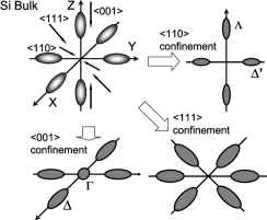
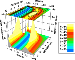
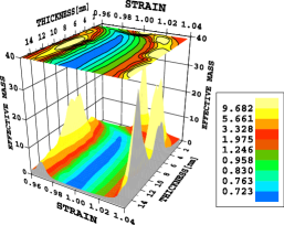
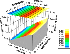
Fig. 2 shows the longitudinal effective mass at the -valley in the [110] confinement as a function of the strain and the slab thickness. The strain is represented by the ratio of the lattice constant under strain to that for the strain-free bulk. The unit of thickness is nm. This figure clearly reveals that along lines, there are two regions with extraordinarily large masses. The confinement causes the contour lines to curve toward the direction of decreaseing strain. This tendency becomes stronger as the thickness decreases. For the [111] confinement, the longitudinal mass distribution is shown in Fig. 3. On the other hand, in the [001]-confined slabs, the behavior of the effective mass at the -valley is very smooth and the variation range of the mass is narrow (0.18 0.20) in Fig. 4. In particular, the effect of confinement is negligibly small. Note that, for the [111] and [110] confinements, a huge mass enhancement is observed in the strain-free region as well as the strained region. To evaluate the surface termination effect, the slab models with the H and Cl atoms for each surface side are investigated and it is found that these models also yield qualitatively the same results as above.
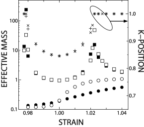
It is reported that the behavior of effective mass for the slab with a thickness more than 10 nm is very similar to that for the bulkYamauchi05 . Fig. 5 shows a comparison between the longitudinal effective mass at the -valley for a slab with 65 Si atomic layer (12 nm) (closed square) and for the bulk (open square) in the strained case. As expected, both behaviors are very similar and reveal a mass divergence at the strains of 0.978 and 1.022. At these strains, the band structure qualitatively changes from double minima to an single minimum. In Fig. 5, the k-position of the minima is plotted for the slab (“+”) and the bulk (“”), where the position is represented by the fractional coordinates and the value 1 corresponds to the Brillouin zone (BZ) boundary. Therefore, the number of electron pockets for the strongly strained bulk changes from six to five. The same analysis is valid for the strained caseYamauchi07 and the number of electron pockets changes from six to three.
When the band with double minima changes into that with a single minimum as a function of one parameter, it can be analytically shown, using the same treatment as Landau’s phenomenological theory for second phase transitions, that the curvature at the minimum becomes zero; that is, the effective mass along the merging direction diverges. Considering the time reversal symmetry, the band with double minima near the BZ boundary along the reciprocal lattice vector is expressed to the lowest order of as where is the parameter used to change the band structure, is the position in the BZ along the vector, and is at the BZ boundary. The k points with the extrema are given by . Assuming that, when , the double minima merge into one, the following condition is obtained: , that is, . This means that the second derivatives of the band energy vanish and the effective mass diverges at .
The mass divergence occurs when the band structure with the double minima changes into that with the single minimum. This band structure change is derived from the strain and confinement.
About the strain for the bulk, it is reported by Ma et al. that the degeneracy of the lowest conduction bands at the point splits due to the (110) and (111) strains but does not do so due to the (001) strain as determined using a semiempirical tight-binding method and group theory Ma91 ; Ma93 . In this study, it is shown that sufficiently strong (111) and (110) strains largely break the symmetry, split the degenerated bands at the BZ boundary, and make the lower band with the single minimum at the BZ boundary, which causes the effective mass anomalies for the thin films and the bulk.
The effect of the confinement on the effective mass anomalies is qualitatively explained as follows. According to the effective mass approximation (EMA), the effect of confinement on the band structure is described by the increase of zeropoint energy , where and are the effective mass along the confinement direction and the thickness, respectively. We extend this EMA expression using the effective mass at the energy minima to the whole band near the BZ boundary. In Fig. 5, the effective mass along the confinement direction [110] at the k-points of 0.84 and 0.95 in the fractional coordinates is plotted using closed and open circles, respectively. The value 0.84 corresponds to the local minima without strain and 0.95 to the neighborhood of the BZ boundary. In the tensile strain region(), the mass at 0.95 is larger than that at 0.84. Therefore, as the confinement thickness decreases, the energy level at the 0.84 increases compared with that at the BZ boundary and the structure with the single minimum is preferable to that with the double minima, which well explains the behavior of effective mass anomalies in Fig. 2. In the compressive region, the same discussion is valid. A similar discussion is found to hold for the confinement case.
For the experimental observation, it is in the confinement case that the effective mass anomalies have the largest effect on the electron transport, because, in the confinement, the anomalies are averaged out by the equivalent valleys along three different directions. For the confinement, there are two kinds of valleys: and , in which the latter does not reveal the anomalies. The parameter region suitable for the observation corresponds to the anomalies where the -valley is the conduction bottom. In the confinement, there are two such regions: that of the thickness range from the bulk to 6 nm and around the 0.98 strain, and that of the thickness range less than 2 nm and the strain range from 0.99 to 1.01. It is experimentally reported that the mobility for channel thicknesses less than 5 nm decreases in the UTBD FET with the -confinedTsutsui05 . This mobility degradation may be due to the effective mass enhancement as well as the surface roughness scattering. When the conduction current is large, the anomaly points where the -valley is energetically higher than the -valley may affect the transport, because the energy difference between the - and -valleys is small (50 meV). For applications that involve, combining piezoelectric devices, the effective mass may be controlled by voltage.
Note that, considering the mechanism of symmetry breaking and confinement, the effective mass anomalies are expected to be found for materials with a similar band structure to Si such as diamond (C), SiC, AlSb, and GaP.
In summary, the effective mass of strained Si thin films and crystals was systematically investigated using first-principles calculations. In and strained Si, effective mass anomalies were found for both the thin films and the crystals. The confinement and the symmetry breaking due to the strain changed the band structure from double minima to a single minimum, which caused the anomalies. In such a case, it was analytically shown that the effective mass diverges. The dependences of the confinement on the anomalies were qualitatively explained by extending the effective mass approximation to the whole band near the BZ boundary. The experimentally observable regions of the strain and thickness were obtained for the confinement.
The author would like to thank Dr. S. Matsuno and Professor K. Shiraishi for valuable discussions. This work was partially supported by a Grant-in-Aid for Scientific Research (Nos. 17064002 and 18063003) from MEXT. Part of this research was carried out through the RSS21 project supported by the Research and Development for Next-generation Information Technology of MEXT. The computations were performed at the Research Center for Computational Science, Okazaki, Japan.
References
- (1) S. Takagi, J. L. Hoyt, J. J. Welser, and J. F. Gibbons, J. Appl. Phys. 96 1567 (1996).
- (2) J. P. Colinge, Silicon-on-Insulator Technology: Materials to VLSI (Kluwer, Boston), 1991.
- (3) K. Uchida, J. Koga and S. Takagi, Tech. Dig. of IEDM, 805 (2003).
- (4) F. Balestra, S. Cristoloveanu, M. Benachir, J. Brini, and T. Elewa, IEEE Electron Device Lett., 8 410 (1987).
- (5) F. Gamiz and M.V. Fischetti, J. Appl. Phys. 89 5478 (2001).
- (6) G. Tsutsui, M. Saitoh, T. Saraya, T. Nagumo, and T. Hiramoto, Tech. Dig. of IEDM, 747 (2005).
- (7) J. Yamauchi: Proc. of the 27-th Int. Conf. on the Physics of Semiconductors, (edited by J. Menéndez and C. G. Van de Walle) 83 (2005); Thin Solid Films, 508 342 (2006).
- (8) J. Yamauchi, Proc. of the 28-th Int. Conf. on the Physics of Semiconductors, Vienna, 2006 (in press).
- (9) Almost at the same time of the conferenceYamauchi07 , the preprint on the effective mass enhancement for the bulk in the tensile strain region using the GW approximation is distributed by the preprint server: D. Rideau, M. Feraille, L. Ciampolini, M. Minondo, C. Tavernier, H. Jaouen, and A. Ghetti (cond-mat/0607510).
- (10) P. Hohenberg and W. Kohn, Phys. Rev. 136 B864 (1964).
- (11) W. Kohn and L. J. Sham, Phys. Rev. 140 A1133 (1965).
- (12) J. P. Perdew and Y. Wang, Phys. Rev. B 45 13244 (1992).
- (13) N. Troullier and J. L. Martins, Solid State Communications 74 613 (1990).
- (14) D. Vanderbilt, Phys. Rev. B 41 7892 (1990).
- (15) The cutoff energy convergence is checked up to 49 Rydberg with respect to the effective mass at the point for the -confined 5-Si-layer slab model. The deviation of the effective mass is within 1%. The convergence of the sampled k-points is evaluated for the response to the biaxial strain in comparison with the calculated values using the doubled mesh for each direction. The relative deviation is within 1% for all confinement directions. The effective mass is less sensitive.
- (16) Landolt-Börnstein vol.17 (Springer-Verlag, Berlin, Heidelberg, New York, 1982).
- (17) J. Yamauchi, M. Tsukada, S. Watanabe, and O. Sugino, Phys. Rev. B 54 5586 (1996).
- (18) In the case of the strained (111) and (110), it is necessary to optimize the internal coordinates, which is described by the internal displacement parameter . The calculated is 0.54 for the both directions, which shows excellent agreement with an other theoretical value 0.53Nielsen85 .
- (19) O. H. Nielsen and R. M. Martin, Phys. Rev. B 32 3792 (1985).
- (20) Some range of data is lacking because of the technical problem that the local density approximation underestimates the band gap and the large strain artificially makes the system metallic.
- (21) Q. M. Ma and K. L. Wang, Appl. Phys. Lett. 58 1184 (1991).
- (22) Q. M. Ma, K. L. Wang, and J. N. Schulman, Phys. Rev B 47 1936 (1993).