Kinetic self-organization of trenched templates for the fabrication of versatile ferromagnetic nanowires
Abstract
We have self-organized versatile magnetic nanowires, i.e. with variable period and adjustable magnetic anisotropy energy (MAE). First, using the kinetic roughening of W(110) uniaxial templates of trenches were grown on commercial Sapphire wafers. Unlike most templates used for self-organization, those have a variable period, 4-12 nm are demonstrated here. Fe deposition then results in the formation of wires in the trenches. The magnitude of MAE could be engineered up or down by changing the capping- or underlayer, in turn affecting the mean superparamagnetic temperature, raised to 175 K so far.
pacs:
68.55.-a, 81.16.Dn, 81.15.Fg, 75.75.+aThe bottom-up approach is promising for the fabrication of nanostructures at moderate cost, with better resolution and less microscopic defects than with lithography. In epitaxial self-organization (SO) the building blocks are atoms that aggregate to each other during growth, a process that can be engineered to fabricate wires and dots with lateral dimensions from the micron size1 down to the atomic size2, 3, 4. The interest of SO for fundamental research is often the narrow size dispersion5, so that macroscopic measurements reveal the properties of one single nanostructure. Issues like the increase of orbital momentum and magnetic anisotropy energy (MAE) at atomic edges or kinks have been addressed2, 3, 5. Concerning applications it is sometimes argued that SO arrays could be used by addressing single nanostructures one by one, to store one bit of information for example. A more realistic view is the use of the array as a material with specific properties arising from the nanoscale. This is the case of semiconductor quantum dots with lasing properties6.
Do magnetic SO systems meet the requirements of applied materials? A prerequisite is that some versatility of geometrical as well as physical properties is achieved, like tuning the magnitude of the MAE. We focus here on the fabrication and properties of wires, which lie at the background of the fast-developing field of spin electronics making use of the propagation of domain walls in wires for storage or logics devices7, 8, 9.
SO magnetic wires are often achieved by step-decoration of vicinal surfaces10, 11, 12. This approach is not versatile as a new crystal has to be prepared with a specific miscut whenever the period needs to be changed. Templates resulting from kinetic effects are potentially more versatile as the period can be changed with processing parameters, like temperature. This has been explored using ion etching under grazing incidence to create ripples on surfaces, independently of crystalline directions14. However a significant control of the period has not been demonstrated so far. Here we explore a new approach, based on the growth of body-centered-cubic (110) materials on nominally-flat Saphir yielding parallel trenches with an adjustable period, which we then use to grow magnetic nanowires. We could tune the magnitude of the MAE of the wires using suitably-chosen capping layers or underlayers. The use of commercial wafers while achieving some control on both the period and the MAE represents a significant advancement in the versatility of SO nanowires.
The samples were grown in a set of ultra-high vacuum chambers using pulsed-laser deposition with a Nd-YAG laser (). The chambers are equipped with a quartz microbalance, sample heating and a translating mask for the fabrication of wedge-shaped samples. A 10 keV Reflection High Energy Electron Diffraction (RHEED) setup with a CCD camera synchronized with laser shots permits operation during deposition. An Omicron room-temperature Scanning Tunneling Microscope (STM-1) and an Auger Electron Spectrometer (AES) are available. The metallic films are grown on sapphire nominally-flat commercial wafers. A detailed description of the chambers and growth procedures can be found in 15. The magnetic measurements were performed ex-situ on 5 nm-Mo-capped samples, with a Quantum Design Superconducting QUantum Interference Device (SQUID) magnetometer.
Ordered arrays of wires were obtained in three steps, consisting of the fabrication of 1. a non-magnetic flat buffer layer; 2. a non-magnetic template displaying a uniaxial array of trenches; 3. Fe wires by layer-by-layer deposition at the bottom of the trenches.
The first step is the preparation of a smooth buffer layer. A seed layer of Mo (nominal thickness ) followed by W () are deposited on sapphire at room temperature (RT) followed by annealing at C. This yields a surface of quality similar to that of metal single crystals, with atomically-flat terrasses of width up to hundreds of nanometers16, 15.
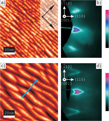
The second step consists of the preparation of a non-magnetic template. It was inspired by reports of the kinetic uniaxial roughening of films of the bcc elements Fe(110)17 and W(110)18 during homoepitaxy at moderate temperature, explained by anisotropic diffusion along the steps and the occurrence of an Ehrlich-Schwoebel barrier. Figure 1a (resp. c) shows the topography of a W(110) layer obtained upon deposition at (resp. following nucleation at and subsequent growth at ). A uniaxial array of trenches aligned along is thus obtained, with a period of (resp. ). The STM cross-sections shown as insets reveal a depth of (resp. 2-3 nm). The structure of the trenches can be probed using RHEED with the electron beam along (Figure 1b,d). The diffraction patterns consist of arrows whose half-angle reveals the slope of the microfacets. The arrows are much sharper for trenches of larger depth because the coherence length along the facets is increased. This allows us to determine accurately the angle of the facets to , in perfect agreement with the triangular-like STM cross-sections of Figure 2c. This angle is unambiguously ascribed to facets of type , with expected. The monitoring of RHEED patterns during growth shows that is a stationary value, reached after a few nanometers of nominal thickness. The occurrence of a stationary angle garanties that the shape of the trenches is not influenced by fluctuations of the width of the trenches, and thus displays essentially no distribution. This is crucial as the dispersion of MAE increases tremendously for nanosized systems in relation with the distribution of structural environments19. The existence of a stationary angle was postulated in Ref.18, however the analysis concluded to facets of type with for W. The discrepancy may come from the fact that the LEED patterns used in Ref.18 were broad because trenches with a small period were studied. We could produce templates with the same facets for Mo, Nb, V and Ta by deposition at room temperature.
The third step consists of the fabrication of wires. Fe is deposited on the templates at (Figure 2), for which layer-by-layer growth occurs with PLD on a smooth surface12, 15. For all deposits we have used W templates, which remain perfectly stable up to . For templates of small period the surface gradually smoothes and becomes essentially flat for (Atomic Layers; not shown here). The details of the early stages of growth are easier to investigate for templates of large period. For these STM cross-sections (Figure 2)b reveal a flat level at the bottom of the trenches, suggesting a progressive filling and thus yielding Fe wires with a triangular cross-section. Disconnected wires can be formed up to , beyond which percolation sets in for the 10 nm period.
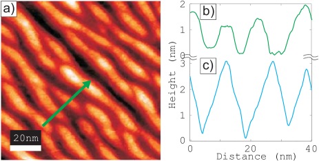
We report below the magnetic properties of Fe wires prepared on W(110) templates with a mean period of 10 nm and an Fe nominal thickness of 2.5 AL. The mean thickness and width of the wires are 1 nm and 7 nm, respectively, as deduced from STM.
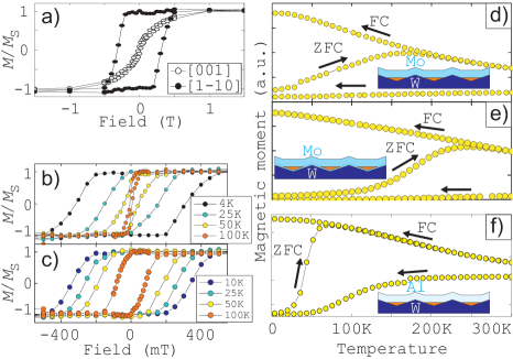
For Mo/Fe/W wires the easy axis of magnetization lies in-the-plane along the wires, i.e. along [001] (Figure 3a). The MAE is deduced from loops along [10] like at . originates from the sum of several contributions, among which only the dipolar energy can be estimated reliably. Other sources of MAE are surface (Néel-type) expected to favor the [10] direction for the (bottom) Fe/W interface20 and [001] for the (top) Mo/Fe interface21, step-edge for Fe/W, expected to favor [10] 10; magneto-elastic – unlike the case of thin films, here the large density of steps is expected to induce a significant out-of-plane mismatch and shear stress, so that no figure or even sign can be reliably predicted; finally the bulk Fe MAE is negligible. Surprisingly for this sample despite this complex situation, similarly to (Fe,Ag) self-organized arrays of wires22.
The loops measured at different temperatures with have a rather square shape, and at remanence full saturation is observed (Figure 3b). The coercivity continuously decreases with temperature while remains essentially unchanged, suggesting a superparamagnetic behavior. The ultimate blocking temperature determined by the ”zero field cooling/field cooling” (ZFC-FC) process is (Figure 3d). The mean value of is around , defined as half-way up the zero-field cooling remagnetization curve.
In the following we report on the use of surface MAE to tailor the magnitude of the MAE of the wires and move towards features that would be required for applications like recording media, like functionality at room temperature and adjustment of MAE. First, the very same wires were fabricated after inserting a -thick underlayer of Mo on the W trenches. The magnetic easy axis is again along the wires, however its magnitude is increased, which is consistent as Fe/Mo interfaces favor alignement of magnetization along 21. This brings the mean from without underlayer to with underlayer (Figure 3e). The coercive field is increased at all temperatures, compare Figure 3b-c. On the reverse is lowered to for Al/Fe/W (Figure 3f).
Conclusion
We have demonstrated a novel route for the self-organization of arrays of planar nanowires on nominally-flat commercial wafers. It is based on the fabrication of a template of trenches upon the deposition under kinetic limitations of a non-magnetic material along a surface of uniaxial symmetry, here W(110), followed by the filling of the bottom of the trenches by a magnetic material under layer-by-layer deposition conditions, here Fe. Periods in the range were demonstrated. Owing to a self-limiting effect the micro-facets are all of type with an angle of , which is promising for attaining a low distribution of physical properties. Concerning magnetism the easy axis of magnetization lies in-the-plane along the wires. We have demonstrated the possibility to tailor its magnitude using interface MAE with different capping- or underlayers, bringing the mean blocking temperature to inserting an ultrathin underlayer of Mo.
B. B. and A. R. acknowledge financial support from French Région Rhône-Alpes (mobility program), and FP6 EU-NSF program (STRP 016447 MagDot), respectively.
References
References
- 1 P. O. Jubert, J. C. Toussaint, O. Fruchart, C. Meyer, and Y. Samson, Europhys. Lett. 63, 135 (2003).
- 2 P. Gambardella, J. Phys.: Cond. Matter 15, S2533 (2003).
- 3 P. Gambardella, S. Rusponi, M. Veronese, S. S. Dhesi, C. Grazioli, A. Dallmeyer, I. Cabria, R. Zeller, P. H. Dederichs, K. Kern, C. Carbone, and H. Brune, Science 300, 1130 (2003).
- 4 J. Repp, F. Moresco, G. Meyer, K.-H. Rieder, P. Hyldgaard, and M. Persson, Phys. Rev. Lett. 85, 2981 (2000).
- 5 N. Weiss, T. Cren, M. Epple, S. Rusponi, G. Baudot, S. Rohart, A. Tejeda, V. Repain, S. Rousset, P. Ohresser, F. Scheurer, P. Bencok, and H. Brune, Phys. Rev. Lett. 95, 157204 (2005).
- 6 Semiconductor Quantum Dots, NanoScience and Technology, edited by Y. Masumoto and T. Takagahara (Springer, Berlin, 2002).
- 7 V. Cros, O. Boulle, J. Grollier, A. Hamzí c, M. Muñoz, L. G. Pereira, and F. Petroff, C. R. Physique 6, 956 (2005).
- 8 D. A. Allwood, G. Xiong, C. C. Faulkner, D. Atkinson, D. Petit, and R. P. Cowburn, Science 309, 1688 (2005).
- 9 S. S. P. Parkin, U.S. patents 6834005, 6898132, 6920062.
- 10 J. Hauschild, U. Gradmann, and H. J. Elmers, Appl. Phys. Lett. 72, 3211 (1998).
- 11 A. Dallmeyer, C. Carbone, W. Eberhardt, C. Pampuch, O. Rader, W. Gudat, P. Gambardella, and K. Kern, Phys. Rev. B 61, R5133 (2000).
- 12 O. Fruchart, M. Eleoui, J. Vogel, P.-O. Jubert, A. Locatelli, and A. Ballestrazzi, Appl. Phys. Lett. 84, 1335 (2004).
- 13 K. Kern, H. Niehus, A. Schatz, P. Zeppenfeld, J. Goerge, and G. Comsa, Phys. Rev. Lett. 67, 855 (1991).
- 14 R. Moroni, D. Sekiba, F. Buatier de Mongeot, G. Gonella, C. Boragno, L. Mattera, and U.Valbusa, Phys. Rev. Lett. 91, 167207/1 (2003).
- 15 O. Fruchart, M. Eleoui, P.-O. Jubert, P. David, V. Santonacci, F. Cheynis, B. Borca, M. Hasegawa, and C. Meyer, J. Phys.: Cond. Matter 19, (2007), in press.
- 16 O. Fruchart, S. Jaren, and J. Rothman, Appl. Surf. Sci. 135, 218 (1998).
- 17 M. Albrecht, H. Fritzsche, and U. Gradmann, Surf. Sci. 294, 1 (1993).
- 18 U. Köhler, C. Jensen, C. Wolf, A. C. Schindler, L. Brendel, and D. Wolf, Surf. Sci. 454-456, 676 (2000).
- 19 S. Rohart, V. Repain, A. Tejeda, P. Ohresser, F. Scheurer, P. Bencok, J. Ferré, and S. Rousset, Phys. Rev. B 73, 165412 (2006).
- 20 U. Gradmann, J. Korecki, and G. Waller, Appl. Phys. A A39, 101 (1986).
- 21 O. Fruchart, J.-P. Nozières, and D. Givord, J. Magn. Magn. Mater. 207, 158 (1999).
- 22 B. Borca, O. Fruchart, and C. Meyer, J. Appl. Phys. 99, 08Q514 (2005).