First-principles calculations of Cu(001) thin films: quantum size effect in surface energetics and surface chemical reactivities
Abstract
First-principles calculations of Cu(001) free-standing thin films have been performed to investigate the oscillatory quantum size effects exhibited in surface energy, work function, atomic relaxation, and adsorption energy of the cesium adsorbate. The quantum well states have been shown and clarified at particular -points corresponding to the stationary extrema in bulk Brillouin zone, which are in good agreement with experimental observations. The calculated surface energetics and geometry relaxations are clearly featured by quantum oscillations as a function of the film thickness of the film with oscillation periods characterized by a superposition of long and short length scales. Furthermore, we have investigated Cs adsorption onto Cu(001) thin films as a function of the film thickness. Our systematic calculated results clearly show the large-amplitude quantum oscillations in adsorption energetics, which may be used to tailor catalysis, chemical reactions and other surface processes in nanostructured materials.
pacs:
73.61.-r, 73.20.At, 73.21.Ac,I Introduction
When the thickness of thin metal films approaches the nanoscale, the oscillatory quantum size effects (QSEs) associated with electronic confinement and interference will occurPag ; Tes ; Mey ; Kaw due to the splitting of the energy-level spectrum into subbands normal to the plane of the films, i.e., the quantum well (QW) states. These QW states lead to strongly modified physical properties and thus have been the subject of numerous experimental investigations in recent yearsChiang2000 ; Milun . For example, the QW states are found to be responsible for an unusual metallic film growth patternHupalo ; Su2001 ; Otero2002 ; Hong2003 , and for the thickness-dependent stabilityLuh2001 observed in the experiment. The QW states are directly connected to the oscillation in the exchange coupling between two magnetic materials across a nonmagnetic spacer layer of various thicknessQiu2002 , and to giant magnetoresistanceBaibich1988 ; Ortega1992 ; Bruno1993 ; Edwards1991 . Moreover, the QW states also give rise to an oscillatory phonon-electron coupling as the film thickness varies, and thus affect the transition temperature of the superconductivityXue1 ; Xue2 .
Experimentally, the characterization of the QW states are commonly measured using angle-resolved photoemission spectroscopy (ARPES) and the scanning tunneling microscopy (STM). ARPES can be used to study the band structure along any direction of the surface Brillouin zone (BZ), while STM offers the possibility to study local structures, such as islands, chains, dots, etc. Using the scanning tunneling spectroscopy (STS) technique, in which the differential conductance () is measured, one can reliably determine the energy of quantized electronic states in the range of approximately 1 eV below and above the Fermi level. Theoretically, a number of approaches have been used in the past in order to describe the electronic properties, in particular the QW states, in ultrathin metallic films. Quasi-one-dimensional models, such as a square well potentialKralj or the phase accumulation model (PAM)Lindgren1987 , have been successfully used to interpret the energies of QW states. More sophisticated methods have also been used, such as the tight-binding approachSmith1994 and layer-Korringa-Kohn-Rostoker approachMoruzzi1978 ; Wang2006 . In a few systems the QW states have been investigated by self-consistent density-functional calculationsFei ; Kie ; Cir ; Boe ; Carlsson2000 ; Wei2002 ; Wei2003 ; Lazic2005 . There are strong reasons to use the ab initio methods. First, there are no adjustable parameters, and a wide range of calculated structural and electronic properties offer the possibility of a detailed comparison with experiments. Also, quantities such as the expected STM profiles and the amplitudes of the wave functions of the QW states, which cannot be obtained in simple approaches, can be calculated.
In this paper we report our first-principles calculations of the QSE in a specific QW system, i.e., the Cu(001) freestanding thin films. Previous QSE studies concerning Cu(001) are mainly focused on the oscillations in magnetic interaction between the two ferromagnetic layers in fcc /Cu/fcc (001) sandwich structures where denotes the ferromagnetic material. It has been demonstrated that the Cu(001) films have a long length scale of 5.6 monolayer (ML) and a short length scale of 2.6 ML of oscillation periods for magnetic coupling in the [001] direction, corresponding to spanning vectors at the belly and neck of the bulk Cu Fermi surface respectivelyD-J ; Cur ; Klsges ; Kawakami . Recent experimental efforts have been focused on the new band structure properties of QW states in Cu(001) systemWu01 ; Danese ; J-M ; Wu02 ; Rotenberg ; Wu03 ; Ling ; Chiara ; Bisio . On the other side, the QSE of Cu(001) associated with its energetics was scarcely considered up to now. In particular, there is no clear experimental or theoretic evidence of the interplay between the different oscillation periods of Cu(001) films by the belly and neck extrema in bulk Cu Fermi surface. In this paper we present a detailed first-principles study of the surface energetics of the Cu(001) free standing thin films. The QW states corresponding to the stationary extrema in bulk BZ are studied in detail. The oscillations of the energetics versus the Cu(001) film thickness are identified and the corresponding oscillation periods are explained. We find that the quantum interference of the QW states with different in-plane wave vectors result in a superposion between long- and short-length oscillating periods.
The other purpose in this paper is to investigate the QSE character in surface adsorption energetics for a representative system in order to shed light on the effect of the QW states on the surface reactivities. Since the adsorption property is closely characterized by the chemical bonding between the adsorbate and the surface of the substrate, thus when the substrate is ultrathin, the QSE in the substrate will also influence the behavior of the surface adsorption. Here we address a particular adsorbate system, i.e., Cs/Cu(001), as a case study to manifest the QSE in surface adsorption properties. Due to its simple electronic structure and active chemical properties which is intrinsic for alkali metals, Cs is a unique adsorbate on metal surfaces, and has been extensively studied. Concerning Cs adsorption on Cu metal surfaces, the recently published articlesBauer ; Ogawa ; Borisov ; Gauyacq ; Corriol ; Hofe mainly focus on the investigation of electronic, dynamic, and geometry properties of Cs layers on Cu(111). The nature of interaction between the Cs adatom and Cu(001) film has been studied both via first-principles pseudopotential calculationsChudinov or through and a jellium model approachWu1990 .
Compared to the previous Cs/Cu(001) work, as mentioned above, our present emphasis is on QSE in surface adsorption energetics, instead of giving a general overview of the nature of alkali-metal-atom adsorption on metal surfaces. In particular, although it has been well known that due to charge transfer from the adsorbed alkali atom to the substrate the alkali adatoms become partially chargedWandelt , the dependence of this charge transfer process on the thickness of the ultrathin substrate film is yet to be understood with high interest. We notice there are emerging some high-quality experimental data of QSE in charge transfer, via observation of the absorbed work function and photoemission as a function of the thickness of the ultrathin substrate filmQiu2007 . Further measurements related with the QSE effect of the adsorption are expected to be systematically reported afterwards due to the availability of the high-quality quantum metal thin films. From this aspect a thorough theoretical investigation is necessary and will be helpful for experimental references in near future. Our results show that in the ultrathin Cu(001) films, the surface adsorption properties display well-defined QSEs.
This paper is organized as follows: In Sec. II, the ab initio based method and computational details are outlined. In Sec. III, the band structure and the properties of QW states at the belly and neck points in bulk BZ are presented. In Sec. IV, the surface properties of the Cu(001) films, surface energy, work function, and interlayer relaxation, as a function of the thickness of the films, are presented and discussed. In Sec. V, the adsorption properties of alkali-metal Cs on Cu(001) surface is discussed in detail by presenting the sensitivity of the adsorption energy to the thickness of the Cu(001) films. Finally, Sec. IV contains a summary of the work and our conclusion.
II Computational method
The calculations were carried out using the Vienna ab initio simulation packageVasp based on density-functional theory with PAW pseudopotentialsPaw and plane waves. In the present film calculations, free-standing Cu(001) films by the so-called repeated slab geometries were employed. This scheme consists in in the construction of a unit cell of an arbitrarily fixed number of atomic layers identical to that of the bulk in the plane of the surface (defining the two dimensional cell), but symmetrically terminated by an arbitrarily fixed number of empty layers (the “vacuum”) along the direction perpendicular to the surface. In the present study we have fixed the whole vacuum region equal to 20 Å, which is found to be sufficiently convergent. The two dimensional unit cell of the fcc Cu(100) surface is a square of edge with basis vectors and where is the Cu bulk lattice constant. The corresponding surface BZ is a square with two high-symmetry directions - and -. During our slab calculations the BZ integration was performed using the Monkhorse-Pack schemePack with a -point grid, and the plane-wave energy cutoff was set eV. Furthermore, the generalized gradient approximation (GGA) with PW-91 exchange-correlation potential has been employed with all atomic configurations fully relaxed. First the total energy of the bulk fcc Cu was calculated to obtain the bulk lattice constants. The calculated lattice constant is Å, comparable with experimentalKittel values of Å, respectively. The use of larger -point meshes did not alter these values significantly. A Fermi broadening of 0.1 eV was chosen to smear the occupation of the bands around by a finite- Fermi function and extrapolating to K.
III Band structure and quantum well states
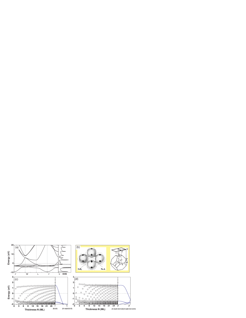
We first studied the properties of electronic structures for bulk Cu and Cu(001) films. For this we have used two kinds unit cells of crystal lattice. Namely, unit cell I is defined via introducing the usual fcc basis vectors , , and , while unit cell II is defined by choosing Cu(001) as the basal plane, i.e., , , and . The volume of second unit cell is twice as that of the first one and it’s convenient to extend to slab calculation since is normal to Cu(001) surface. Correspondingly, the reciprocal lattice basis vectors are , , and for unit cell I and , , and for unit cell II. Figure 1(a) shows the band structure and the DOS of bulk fcc Cu (unit cell I). The highly dispersive - band, typical of noble metals, is present. The more intense band region is located between 2.0 and 4.5 eV below Fermi surface and can be measured by a large rise of the intensity in photoemission experimentsQiu2002 . The - hybrid band region with two less intense dispersive states can also be seen in Fig. 1(a). The Fermi surface of bulk Cu and the Brillouin zone for unit cell I are schematically shown in Fig. 1(b). Of particular interest for Cu(001) thin film studies are the two extremal points, i.e., the belly and neck points at the bulk Fermi surface. Previous extensive studies have shown that the stationary spanning vectors connecting the belly and neck points respectively play a key role in determining the oscillatory behavior of interlayer magnetic exchange interaction in fcc /Cu/ (001) sandwich structures where denotes the ferromagnetic material. The belly extrema was found to correspond to long oscillating period in while the neck extrama corresponds to short period.
One inconvenience in discussing properties of Cu(001) film via the bulk Fermi surface calculated from unit cell I lies in the fact that none of three basis vectors of unit cell I is normal to (001) surface, which leads to an oblique projection of bulk BZ onto (001) surface BZ. On the contrary, by use of unit cell II the discussions, particularly for QW states of (001) thin films, become very convenient. Beginning with this unit cell construction, the belly point in bulk BZ is still projected to point, like with unit cell I. Whereas the neck point, after projection, turns to be at line. In this paper the neck point will be named and for bulk and surface BZ (with respect to unit cell II) respectively. Our band structure calculation gives the position [in coordinates of ()] of to be .
Now we turn to study the electronic structure of Cu(001) thin film with focus on QW states. Since the previous studiesQiu2002 have shown that the long and short oscillating periods in interlayer magnetic exchange interaction originate from band dispersions at and points respectively, we expect the other intrinsic film properties such as film energetics, atomic structure relaxations, and even surface chemistry are closely related with the QW states at these two kinds of stationary -points. Figure 1(c) shows the energies of the QW states at point as a function of the film thickness without interlayer relaxation. The energy zero is set at the Fermi level of each film. Interlayer relaxation effect is also studied and it is found that the overall thickness dependence of the energies are similar to that without relaxation. For comparison, also plotted in Fig. 1(c) (right panel) is the energy dispersion in the bulk along [001] () direction, which corresponds to the center of (001) surface BZ and determines the energy range for the QW states shown in the left panel. One can see from Fig. 1(c) that as the thickness of the film increases, the energy of a given QW state also increases. When the thickness of the film is increased to be about 5.0 monolayers, then a quantum well state, with the energy crossing the Fermi level, occurs. The next energy crossing with the Fermi level occurs at the film thickness of 11 monolayers. Our calculated result of quantum well states is in good agreement with the recent experimental ARPES measurementQiu2002 , in which the photoemission intensity as a function of energy for fixed Cu thickness and as a function of Cu thickness for fixed energy clearly show the existence of the QW states of the electrons in the Cu layer. Fig. 1(d) shows (left panel) the energies of the QW states at point as a function of film thickness without interlayer relaxation. The energy zero is set at the Fermi level of each film. Again the bulk energy dispersion along [001] direction (starting from point). One can see that for every incremental increase in the film thickness of about 2.6 ML, then a new quantum well state crosses the Fermi level. A comparison between the left panel and right panel in Fig. 1(c) [or (d)] shows that the bulk electron band of Cu works very well for QW states as the Cu thickness is greater than 5 ML, which agrees well with the experimental resultsKawakmi1998 .
The quantitative understanding of the QW states showed in Figs. 1(c)-(d) is usually analyzed using the so-called phase accumulation model (PAM)Ech ; Smith . Here the free standing Cu(001) film is considered as a quantum well confining electrons between the two vacuums in the slab. Since the system is invariant on translation parallel to the (001) plane, the in-plane wavevector is a good quantum number. Thus, for a given , the quantization condition for an electron state in such a well is given by
| (1) |
where is the number of atomic layers in the film, the interlayer spacing, is the phase gain of the electron wave function upon reflection at the the film-vacuum interface, is the number of half-wavelengths confined inside the QW and describes the Cu electron wavevector component along [001] direction for the th QW state. Equation (1) has been successfully used to model QW states in metal thin films, and its validity has been rigorously tested by full-scale first-principles calculations for some special systemsWei2002 . It should be addressed that QW states will not only form at the point but also form in a large part of the surface BZ, and the quantization condition (1) may be applied throughout the entire zone. Using Eq. (1) one can calculate the periodicity for the QW states crossing the Fermi level, , where is the bulk Fermi wavevector along [001] direction for a given in-plane wavevector . For the point (), from the right panel in Fig. 1(c), one can see that the upper branch of the bulk band runs through of the BZ, . One gets . Therefore a new QW state of occurs every ML increase of the film thickness, which is verified in the left panel in Fig. 1(c) that an energy branch moves down, crossing the Fermi level for every incremental increase in the film thickness of layers. Similarly for point corresponding to in bulk BZ, one can derive from the right panel in Fig. 1(c) . In this case, Eq. (1) gives the periodicity for the QW states to be . Therefore, Figs. 1(c)-(d) reveal that the periodic behavior of the Cu(001) QW states is essentially governed by the bulk Cu electronic structure properties. In particular, the extremal points of the Fermi surface and the extremal points of the QW branches close to the Fermi level occur at the same , i.e., at in the bulk BZ corresponding to in the (001) surface BZ and at the neck extrema both in the bulk BZ and in the surface BZ. This relationship between the Fermi surface and the quantum-well dispersion turns out to be very fruitful for the understanding of the connection between the periods in energetics and surface reactivity discussed below.
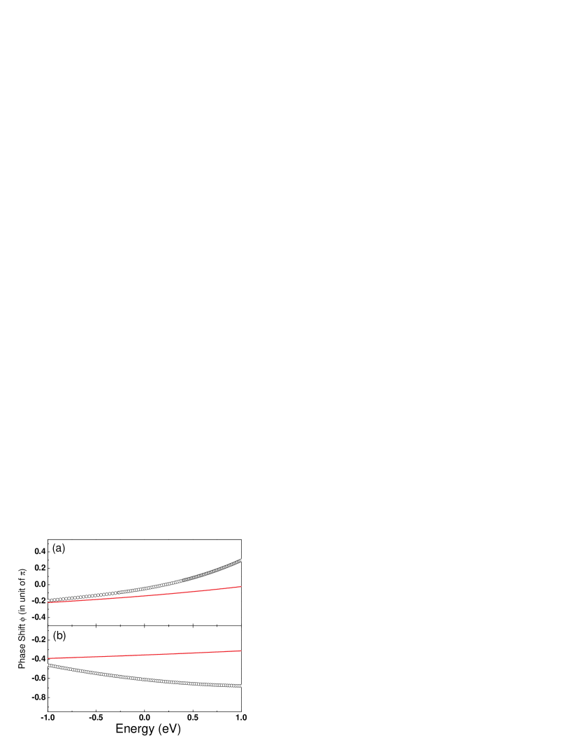
Using the energy data for QW states in Figs. 1(c)-(d), and with the help of Eq. (1) and the bulk band structure shown in the right panels in Figs. 1(c)-(d), one can deduce the phase shifts for the QW states at and points. They are plotted as filled circles in Fig. 2(a)-(b) respectively. Since the energy range of interest is quite far from the calculated vacuum level of 4.5 eV (relative to the Fermi level), this phase shift curve is nearly featureless for most of the energy range, except for the feature near the top of the band. In general the phase shift depends on the incident (with respect to the film/vauum interface) energy and momentum of the electron. A simple expression obtained from the WKB approximation is often used in the literature and has the formMcRae
| (2) |
Here 4.5 eV is the Cu work function (in the thin thickness limit), is the electron energy measured from the Fermi level and is the the in-plane wavevector of QW. The image potential due to the electron–hole attraction is like a one-dimensional hydrogen atom. That is where the 3.4 eV is from which actually equals one quarter of the hydrogen ionization energy. For the belly of the Cu Fermi surface while for neck point we obtain Å-1. Equation (2) is plotted as a dashed curve in Fig. 2. Note that the data points within a given energy range can come from films of very different thickness. The datasets at both and vary smoothly as a function of energy with little scattering, indicating that Eq. (1) does determine the energies of the QW states quantitatively, provided the phase shifts are known.

The energies of QW states near the Fermi level can be measured by STS experiments, in which the local density of states (LDOS) is probed through the d/d curve. The distinctive sharp peaks in d/d curve are characteristic of the QW states at different quantum numbers. The most easy-to-see quantity in STS measurement is the energy gap between the highest occupied QW state and lowest unoccupied QW state. To see the thickness dependence of , taking the derivative of Eq. (1) with respect to energy and evaluating it at the Fermi level for a given , one hasWei2002
| (3) |
where is the Fermi velocity obtained from the slope of the bulk band at the Fermi level and the energy derivative of the interface electronic phase shift at the Fermi level. Therefore, the measured curve is a linear function of , with a slope connected to . Figure 3 shows the calculated at and points using the QW energies in Figs. 1(c)-(d). One can see that the two curves follow a straight line with different slopes. Also it can be seen that whence a new branch of QW states crosses the Fermi level, then a kink occurs. Due to the different periods at and , the kinks in these two curves are also located at different values of . Note that the intersection of the linear curves with the horizontal axis is not necessarily at , due to the nonzero energy derivative of the interfacial phase shifts at the Fermi levelWei2003 .

Another central quantity closely related with above discussed QW electronic structure of Cu(001) thin film is the film electronic DOS at the Fermi level, . As shown in Fig. 4, the film with respect to the film thickness displays well-defined oscillations with oscillation periods characterized by a superposition of long and short length. Note that in obtaining Fig. 4 we have increased the -grid for integration to for each value of , which ensures the precision of the result. The oscillations in give an periodic band energy contribution to the total energy, thus producing oscillatory surface energetics and reactivity which will be shown below.
IV Film energetics and interlayer relaxation
Figure 3(a) shows the total energy per monolayer as a function of the number of layers in the slab. The atoms in the slabs have been fully relaxed during the calculations. One can see from Fig. 3(a) that with increasing the thickness, gradually approaches a constant value which in the limit is equal to the energy per atom in bulk Cu.
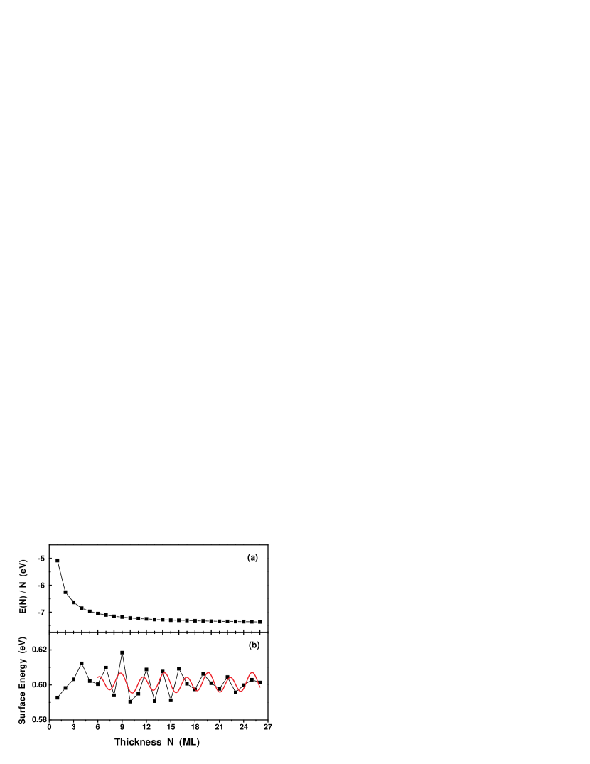
An energetic quantity more suitably tailored to QSE is the surface energy which is defined as one-half of the energy difference between the film and the bulk with the same number of atoms, including the proper subtraction of a term linear in Boe2 . The thickness dependence of surface energy is calculated and shown in Fig. 3(b) (curve with squares). It reveals that the surface energy approximately follows a periodic oscillatory form, in accord with the oscillation properties of film . This can be simply reasoned by the fact that the total band energy with respect to the Fermi level is related to the DOS by the equation . Therefore, each time the total DOS crosses the Fermi level, the band energy will also as a response have an oscillatory change, which consequently results in periodic oscillations in surface energy. In the same manner as discussed above, one can expect that the oscillations in the surface energy consist of a superposition of oscillations with the periods corresponding to the extremal points of the bulk Fermi surface. To illustrate this, also plotted in Fig. 3(b) (red curve) is a least-squares fit to the surface energy with the following expression
| (4) |
where is the number of monolayers (ML), and are the periodicities (in unit of atomic ML) corresponding to the bell and neck extrema in bulk Cu Fermi surface, and are the fitting parameters. It can be seen that the fitting curve well reproduces the oscillating behavior in the surface energy. Thus the periods extracted from the calculated Cu(001) surface energy are well consistent with the periods extracted from the bulk Fermi surface, and again the stationary extrema in Fermi surface play a key role in determining the oscillatory behavior in surface energetics.

Some authors have used the energies of QW states at to discuss the stability of the film. See Ref.Wei2003 for an example. The key point employed there is that even though the confinement takes place only in one of the three dimensions, the stability of the film could also be affected due to the variation in the electronic energyZhang . In the present case, since the above discussions have clearly shown that the neck point in the bulk Fermi surface plays the same important role as the bell point (corresponding to in surface BZ) does in determining the oscillatory energetics properties of Cu(001) thin film, thus one can reasonably expect that the stability of the film also exhibits a superposed oscillatory behavior as a function of the film thickness, with the oscillation periods consisting of long and short length. To illustrate this, following Ref.Wei2003 , we use the second difference of the total energy as a measure of the relative stability of an -layer film with respect to the films of and layers, which is defined as
| (5) |
where is the calculated total energy of the fully relaxed -layer film with the in-plane lattice constant fixed at the theoretical value. The result is shown in Fig. 5. A peak in the figure indicates a high relative stability for the film. It is not surprising that the stability is featured by a superposition of long- and short-period oscillations as is evident from the discussion above. Remarkably, one can see the film is mostly stable while the film is particularly unstable.

In addition to the surface energy, we have also calculated the work function of freestanding Cu(001) thin film. The work function, defined as the minimum energy required to emit an electron from the surface to the vacuum, is one fundamental physical quantity for surface reactivity. An elementary picture of the work function involves a surface dipole layer that a valence electron must overcome in order to escape. Since the work function, as with many other properties, is also a function of the electronic density, thus the changes in the electronic density by the crossings between the QW states and Fermi level will influence the work function in an oscillatory way. In addition to its relevance as an important element in our understanding of surface science, a modified, or tunable, work function can be useful for applications such as catalysis, because a slight change in the energy scale is exponentially amplified for chemical reactionsTang2002 . Recent in situ experiments have measured atomic-layer-resolved work function and shown clear QSE in Ag/Fe(100)Paggei2002 and Pb/Si(111)Xue2007 systems. Here we have carried out first-principles calculations of the work function of the clean Cu(001) surface. The result is shown in Fig. 7(a) (filled squares) as a function of film thickness with relaxed atomic geometry. One can see that the work function is featured by an oscillatory behavior. As with the surface energy, the oscillations in the work function of Cu(001) thin films consist of a superposition of long- and short-length periods.
| 2 | -5.186 | |||||
|---|---|---|---|---|---|---|
| 3 | -3.351 | -3.350 | ||||
| 4 | -3.131 | +0.616 | -3.144 | |||
| 5 | -3.425 | +0.081 | -0.099 | -3.431 | ||
| 6 | -2.798 | +0.477 | -0.213 | +0.487 | -2.800 | |
| 7 | -4.076 | +0.126 | +0.398 | +0.394 | -0.115 | -4.066 |
| 8 | -2.693 | +0.189 | -0.320 | -0.066 | -0.317 | +0.185 |
| 9 | -2.917 | +0.369 | +0.133 | +0.484 | +0.492 | +0.134 |
| 10 | -3.358 | +0.343 | -0.364 | +0.039 | -0.335 | -0.042 |
| 11 | -2.805 | +0.415 | +0.256 | +0.415 | -0.029 | -0.025 |
| 12 | -3.279 | +0.296 | -0.274 | +0.382 | -0.219 | -0.498 |
| 13 | -3.699 | +0.237 | -0.322 | -0.134 | -0.407 | -0.938 |
| 14 | -2.968 | +0.469 | +0.019 | +0.177 | -0.041 | +0.037 |
| 15 | -3.286 | +0.127 | -0.315 | -0.245 | -0.721 | -1.015 |
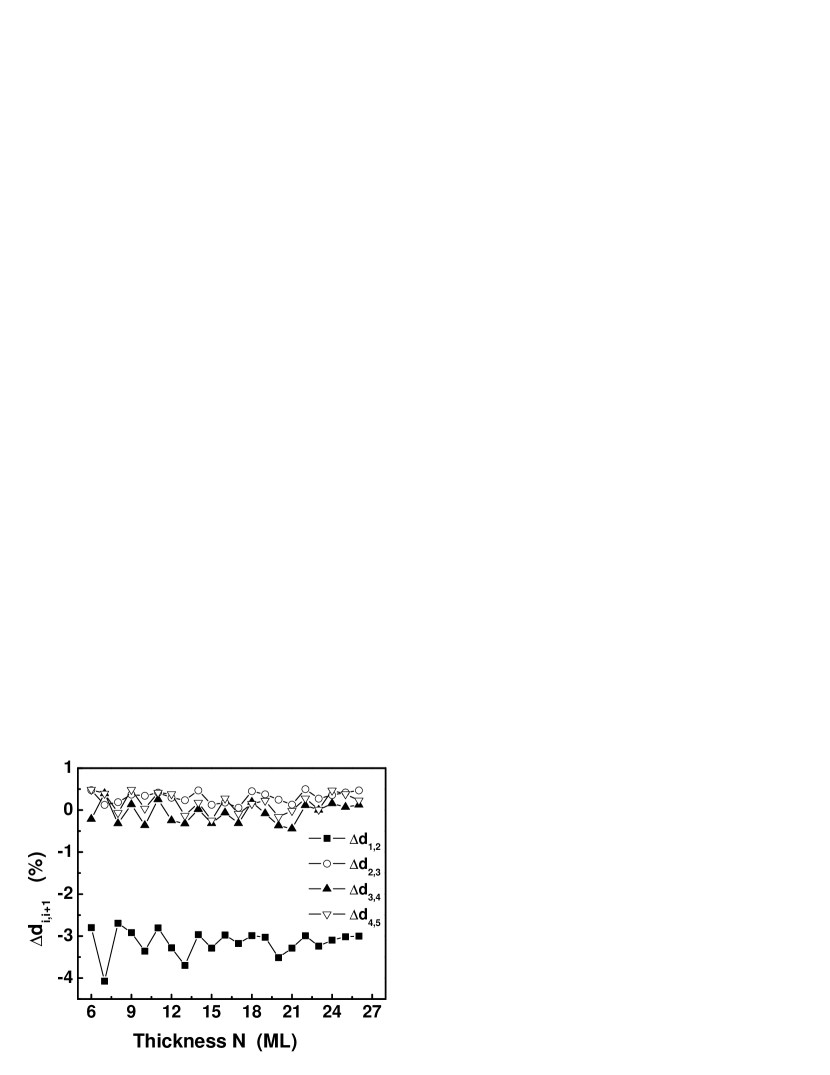
In addition to the above discussed film energetics, the relaxed atomic structures of the Cu(001) thin film will also be influenced by the occurrence of QW states at the Fermi level. Since the supercells are employed and is a good quantum number, thus only atomic interlayer relaxation along [001] direction is allowed during our calculations. Here the interlayer relaxation, , is given in percent with respect to the unrelaxed interlayer spacings, , i.e., . is the interlayer distance between two adjacent layers parallel to the surface calculated by total energy minimization. is the bulk interlayer distance along [001] direction. Obviously, the signs and of indicate expansion and contraction of the interlayer spacings, respectively. The interlayer relaxations of Cu(001) films as a function of the film thickness is summarized in Table I. Furthermore, the interlayer relaxations are also plotted in Fig. 8 as a function of for clear illustration. One can see: (i) The two outmost layers relax significantly from the bulk value, in agreement with the result from FLAPW calculationSilva02 . In the whole range of layers that we considered, the topmost interlayer relaxation is always inward (), with starting from the largest value of -5% for a slab with only two monolayers, and approaches a final value of -3% with increasing the thickness of Cu(001) films. Whereas, the second interlayer relaxation is always outward (). Note that the first interlayer separation on most metal surfaces is contracted, Cu(001) is one of the typical examples. (ii) The interlayer spacings oscillate as a function of the thickness of the film with the period again consisting of long- and short-length scales. After 26 monolayers, which is the maximal layers considered here, the oscillations are invisible which suggest that the semi-infinite surface limit is now reached.
V Adsorption of cesium: QSE in surface cesiation
In the above discussions we have extensively studied the QW states in Cu(001) thin films and the corresponding QSE in various physical quantities such as the surface energy, work function, and interlayer relaxation. To further illustrate the physical properties influenced by finite size of the thin films, in this section we focus our attention to the adsorption of Cs on Cu(001) thin films. Note that our study in this section is not just for an alternative verification of QSE in solid thin film. On the contrast, the present study of surface adsorption as a function of the film thickness has its own cause to be emphasized. It is well known that metal surfaces are a prototype heterogeneous catalyst, and have been widely studied in terms of the dissociative chemisorption of the reactant molecules. For a given solid, except for surface irregularities such as steps and defects, its surface reactivity is almost solely determined by the crystallographic orientation. At reduced size and/or dimensionality, particularly when the characterized size enters nanometer scale, however, the situation could be dramatically different from that of the bulk. In fact, size-dependent surface chemical activities in metal films with the thickness of nanometer scale have been observed in previous experimental reportsDanese2004 ; Aballe2004 . Remarkably, in a very recent oxygen adsorption experiment on high-quality Pb(111) thin films, Ma et al have clearly observed an oscillatory dependence of the chemical reactivities on the film thicknessXue2007 , thus providing a most convincing proof of the key role played by the QW states in changing surface reactivity. It is expected that more experiments will address the issue of QSE in surface chemical reactivities. From this aspect, the present detailed theoretical analysis for the dependence of behavior of Cs adsorption upon the Cu(001) film thickness is highly interesting and will be helpful for experimental reference in near future.

Before we study the Cs adsorption properties as a function of the thickness of Cu(001) thin films, we need to determine the energetically favorable adsorption site. Since the preference of adsorption site is not sensitive to the thickness of the substrate, thus to look for this preference of the adsorption site, it is sufficient to give a study on the slabs with fixed thickness of the Cu(001) substrate, which at present is chosen to be 5 ML. We choose four most probable adsorption sites, which is enumerated in Fig. 9. The binding energy is calculated using the following equation: Binding energy [atomic Cs](Cs/Cu(001)Cu(001)Cs)/2 where Cs/Cu(001) is the total energy of a slab which includes two Cs atoms inside with a symmetric configuration, Cu(001) is total energy of the slab without Cs atoms, and Cs is total energy of a free Cs atom which is put in a 16 Å16 Å16 Åsupercell. The calculated Cs/Cu(001) binding energies are 0.9189 eV, 0.9176 eV, 0.9174 eV, and 0.9327 eV for site-1, site-2, site-3, and site-4 respectively. Thus site-4 is most stable for adsorption. This is in accord with recent experiments that for substrate surfaces with square or rectangular symmetry the alkali atoms occupy adsorption sites which maximize the coordination number to the substrateBerndt ; Andersson ; Demuth ; Eggeling ; Aminpirooz ; Muschiol ; Mizuno . Thus in the following the atomic Cs is always put on site-4 during the simulation. This adsorption site is independent on the coverage of Cs atoms. In this paper, we only consider the case of .
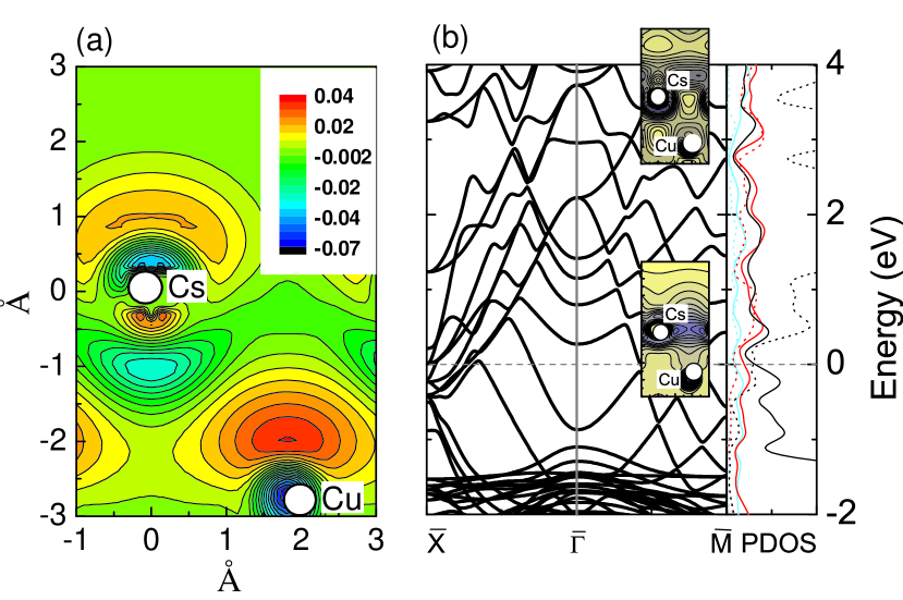
To illustrate the surface bond formed between Cs adatom and Cu surface atoms, we depict in Fig. 10(a) the contour map of the electron-density difference for Cs/Cu(001). Here the plane depicted is normal to the surface and contains a Cs and two Cu’s. The density difference was obtained by subtracting the densities of noninteracting component systems, Cu(001)Cs, from the density of the Cs/Cu(001) system, CsCu(001), while retaining the positions of the component systems at the same location as Cs/Cu(001). The solid and broken lines denote an increase and decrease, respectively, in electron density upon Cs adsorption onto the surface. Covalent bonding is evident from the accumulation of the charge between the Cs adsorbate and the Cu(001) substrate. This charge is drawn principally from the atomic 6 state of Cs adlayer. On the vacuum side of the overlayer the charge is depleted. Thus the Cs 6 state causes a polarization toward the Cu(001) surface. As a response, the work function will be decreased by this occurrence of surface polarization. On the other side, a significant counter-polarization of the Cs 5p semicore charge is also quite evident from Fig. 10(a). This effect opposes the reduction of the work function and the ultimate value of work function represents a self-consistent compromise between 6 and 5 polarization. The net result of these multiple surface dipoles, as shown in Fig. 7(b), is a lowering of the work function upon cesiation from 4.473 eV [clean ten-layer Cu(001) slab] to 2.259 eV for the coverage , corresponding to the relaxed height of the Cs atom above the Cu film of 2.988 Å. Also due to this opposite orientation between 6 and 5 polarization, the work function of Cs/Cu(001) displays a non-monotonic variation with increasing the coverage of Cs: At low coverage, the work function decreases with increasing the coverage, going through a minimum (about at ) and increases a little bit from there on to the high coverage valueArena1997 . The similar picture of cesiation process has largely discussed in Cs/W(001) systemWimmer1983 . A well-know conclusion in studying alkali-metal-atom chemisorption onto a metal surface is that although the region around the alkali-metal adatom is electrically neutral and no net charge transfer towards the metal surface is exhibited, the electrons of the alkali-metal adatom undergo a strong mixing with the substrate electron orbitals during the adsorption process. Such a process is local around the adatom and accompanied by a screening process, which is responsible for work function change. Furthermore, Figure 10(b) shows the band structure (left panel) and the orbital-resolved local DOS (right panel) for the Cs adatom and surface Cu atom, respectively. The complex Cs-induced charge rearrangement is more obvious. The Cs adatom experiences during adsorption a repulsive interaction of the valence electron with the induced image charge of the ionic nuclear core. As a result, the valence electrons shift upward in energy and hybridize with those of the substrate into bonding and antibonding statesNordlander ; Ishida . The bonding states are mainly around the Fermi level and are dominated by hybridization between adatom and surface Cu orbitals, as shown in the lower panel in the inset in Fig. 10(b). Whereas, the antibonding states shift up away from the Fermi level with a typical value of 3.8 eV, and largely consists of hybridization between Cu and Cs orbitals, which can be seen from the upper panel in the inset in Fig. 10(b). A thorough description of the bonding properties in Cs/Cu(001) system is beyond our intention in this paper.

After finding the preferred atomic Cs adsorption site [site-4 in Fig. 9] and getting familiar with the Cs-Cu(001) bonding properties, we turn now to our central focus on the QSE in surface chemisorption and reactivity. For this purpose, we have given a series of calculations for the binding energy (the reverse of the adsorption energy) of the Cs adsorbate as a function of the thickness of Cu(001) thin films. Here as mentioned above we only consider the case of . The results are depicted in Fig. 11(a). One can see that the binding energy of Cs onto Cu(001) thin films depends on the film thickness in a damped oscillatory way. These oscillations are featured by a superposition of long- and short-length periods, thus indicating a well-defined QSE in the surface chemical reaction of Cu(001) thin film with respect to Cs adsorption. In experiment this QSE of atomic adsorption can be observed by investigating the dependence of Cs coverage on the monolayers of Cu(001) thin films. We address here that the calculated data in Fig. 11 have been carefully checked. This ensures that the oscillating behavior of the adsorption energy has nothing to do with the convergence problem, which may be encountered in the cluster calculations. The supercell approach retains 2D periodic boundary conditions during calculation, and can avoid this problem. Therefore, as with other quantities, the oscillations in adsorption energy is physically caused by the periodic change in the DOS at . In fact, from what we have shown in Figs. 10, or from the simplest Anderson-Grimsley-Newns adsoptin modelNewns ; Norskov , one recalls that as a Cs atom approaches to the Cu(001) surface (which can be approximated by a free-electron-like metal), the valence - states of Cs adatom are broaden into resonant states due to as a result of interaction with the metal bands. Surface electrostatic potential will shift this hybridization down in energy to below for sustaining the whole neutralization. A lower DOS at implies that the Cu(001) film has fewer electronic states to respond, whereas a higher means the film has more electronic states to respond, to the presence of the Cs adsorbate. Therefore, higher implies higher probability in the above hybridization process, causing the resonance to move to lower energies and to be occupied. This leads to a higher surface reactivity and higher adsorption energy. This physical picture can be formulated by expressing the adsorption energy as
| (6) | ||||
where un-adsorbed is the band energy for a combined Cs/Cu(001) system with Cs adatom and Cu(001) film largely separated such that no chemsorption occurs, adsorbed is the band energy for the adsorbed Cs/Cu(001) system, DOSun-adsorbed DOSadsorbed is the difference in the electronic DOS between the un-adsorbed and adsorbed Cs/Cu(001) systems. As the film thickness changes, QW state energy levels shift. Whenever a QW state crosses the Fermi level from above, it adds energy to the un-adsorbed and adds electronic density to un-adsorbed . Whereas adsorbed decreases upon the crossing between the QW states and the Fermi level due to the above mentioned cause that the Cs-Cu orbital hybridization shifts more down in energy by the increase of . Thus the net consequence is an anti-phase oscillation mode of the adsorption energy with respect the oscillation mode of as a function of the film thickness.
The Cs adsorbate height is plotted in Fig. 7(b) as a function of the film thickness, which also shows the periodic oscillations indicative of QSE. Compared to the features in thickness dependence of binding energy, one can notice that oscillations in the adsorbate height are much weak and the periods are somewhat not easily resolved. The cause may be due to the fully interlayer relaxations as a whole structure during calculations. If the substrate is not allowed to relax during the adsorption process, then it can be expected that there is a consistent correspondence in the oscillations between the binding energy and the height of the adsorbate.
Moreover, we have also calculated the work function of Cs/Cu(001) as a function of the film thickness. The results are shown in Fig. 7 (open squares). Compared to the case of clean Cu(001) films, the work function is decreased by a typical value of 2.2 eV [see Fig. 7(b) for 10-layer case]. Also, the adsorbed work function oscillates with increase of the film thickness. However, one can see that the oscillating mode is different from that without adsorption, and also the oscillating amplitude becomes much weak. This implies that the QW states are different for clean and cesiated Cu(001) thin films. As a result, there no longer exists a simple one-to-one correspondence between the adsorbed QW states and the bulk Cu Fermi surface. More detailed work will be done for this issue.
VI Conclusion
In summary, the clean and cesiated Cu(001) thin films have been extensively studied by density-functional theory pseudopotential plane-wave calculations. The dependence of electronic structure, surface energetics, and interlayer relaxation upon the thickness of the film has been fully investigated, clearly showing the metallic QSEs of the film. These QSEs have been shown to be closely related with the occurrence of QW states at the Fermi level. Unlike some other simple metals such as Al, Mg, and Pb, the Fermi surface of bulk Cu is characterized by multiple stationary extrema such as the belly and the neck points. As a consequence, the Cu(001) QW states also display the abundant properties at these surface-projected -extrema. For example, we have shown the different film-thickness oscillation modes by calculating the energies of QW states in correspondence with these stationary extrema. Due to the interference between these two kinds QW states, the energetics and the corresponding stability (Fig. 6) of the Cu(001) thin films have been shown in a consistent way to display a quantum beating behavior as a function of the film thickness, with the oscillation periods consisting of long and short length. In addition, the calculated energy gap between the highest occupied QW state and lowest unoccupied QW state, which can be directly measured via STS technique, have been shown to display different slopes and kinks at these extrema in bulk BZ.
We have also extensively discussed the other highly interested issue, i.e., the oscillatory QSE in surface chemical reactivities, via studying the Cs adsorption onto the Cu(001) thin films. Through systematic calculations, we have shown that the Cu(001) surface chemical catalysis for Cs adsorption can be uniquely modulated and controlled by the occurrence of QW states at the Fermi level. The Cs adsorption energy and the work function after cesiation are featured by quantum oscillations as a function of the film thickness. The amplitudes in these oscillations reach a typical value of 40 meV. From the application point of view, this result is quite intriguing because 1ML change in the film thickness can cause an effect equivalent to a temperature change as high as 400 degrees. These calculated results thus may be used as a guide to tailor catalysis, chemical reactions and other surface processes in nanostructured materials.
Acknowledgements.
This work was partially supported by the CNSF under Grant No. 10544004 and 10604010.References
- (1) J.J. Paggel, T. Miller, and T.-C. Chiang, Science 283, 1709 (1999).
- (2) Z. Tesanovic, M.V. Jaric, and S. Maekawa, Phys. Rev. Lett. 57, 2760 (1986).
- (3) A. E. Meyerovich and S. Stepaniants, Phys. Rev. Lett. 73 316 (1994).
- (4) A. Kawabata, J. Phys. Soc. Jpn. 62, 3988 (1993).
- (5) T.-C. Chiang, Surf. Sci. Rep. 39, 181 (2000).
- (6) M. Milun, P. Pervan, and D. P. Woodruff, Rep. Prog. Phys. 65, 99 (2002).
- (7) M. Hupalo, S. Kremmer, V. Yeh, L. Berbil-Bautista, and M.C. Tringides, Surf. Sci. 493, 526 (2001); M. Hupalo and M.C. Tringides, Phys. Rev. B 65, 115406 (2002).
- (8) W.B. Su, S.h. Chang, W.B. Jian, C.S. Chang, L.J. Chen, and T.T. Tsong, Phys. Rev. Lett. 86, 5116 (2001).
- (9) R. Otero, A.L. Vázquez de Parga, and R. Miranda, Phys. Rev. B 66, 115401 (2002).
- (10) H. Hong, C.M. Wei, M.Y. Chou, Z. Wu, L. Basile, H. Chen, M. Holt, and T.-C. Chiang, Phys. Rev. Lett. 90, 076104 (2003).
- (11) D.-A. Luh, T. Miller, J.J. Paggel, M.Y. Chou, and T.-C. Chiang, Science 292, 1131 (2001).
- (12) For a review, see Z.Q. Qiu and N.V. Smith, J. Phys.: Condens. Matter 14, R169, and references therein.
- (13) M.N. Baibich, J.M. Broto, A. Fert, F. Nguyen Van Dau, F. Petroff, P. Etienne, G. Creuzet, A. Friederich, and J. Chazelas, Phys. Rev. Lett. 61, 2472 (1988).
- (14) J.E. Ortega and F.J. Himpsel, Phys. Rev. Lett. 69, 844 (1992).
- (15) P. Bruno, J. Magn. Magn. Mater. 121, 248 (1993).
- (16) D. M. Edwards et al., Phys. Rev. Lett. 67, 493 (1991).
- (17) Y. Guo, Y.-F. Zhang, X.-Y. Bao, T.-Z. Han, Z. Tang, L.-X. Zhang, W.-G. Zhu, E.G. Wang, Q. Niu, Z.Q. Qiu, J.-F. Jia, Z.-X. Zhao, and Q.-K. Xue, et al., Science 306, 1915 (2004).
- (18) Y.-F. Zhang, J.-F. Jia, T.-Z. han, Z. Tang, Q.-T. Shen, Y. Guo, Z. Q. Qiu, and Q.-K. Xue, Phys. Rev. Lett. 95, 096802 (2005).
- (19) M. Kralj, A. Šiber, P. Pervan, M. Milun, T. Valla, P. D. Johnson, and D. P. Woodruff, Phys. Rev. B 64, 085411 (2001).
- (20) See, for example, S.Å. Lindgren and L. Walldén, Phys. Rev. Lett. 59, 3003 (1987).
- (21) N. V. Smith, N. B. Brookes, Y. Chang, and P. D. Johnson, Phys. Rev. B 49, 332 (1994).
- (22) V. L. Moruzzi, J. F. Janak, and A. R. Williams, Calculated Electronic Properties of Metals (Pergamon, New York, 1978).
- (23) Y. Wang, Z.-Y. Lu, X.-G. Zhang, and X.F. Han, Phys. Rev. Lett. 97, 087210 (2006).
- (24) P.J. Feibelman, Phys. Rev. B 27, 1991 (1983).
- (25) A. Kiejna, J. Peisert, and P. Schraroch, Surf. Sci. 432, 54 (1999).
- (26) S. Ciraci and I.P. Batra, Phys. Rev. B 33, 4294 (1985); I.P. Batra, S. Ciraci, G.P. Srivastava, J.S. Nelson, and C.Y. Fong, Phys. Rev. B 34, 8246 (1986).
- (27) J.C. Boettger and S.B. Trickey, Phys. Rev. B 45, 1363 (1992); U. Birkenheuer, J.C. Boettger, and N. Rösch, Chem. Phys. Lett. 341, 103 (1995); K.F. Wojciechowski and H. Bogdanów, Surf. Sci. 397, 53 (1998); K. Doll, N.M. harrison, and V.R. Saunders, J. Phys.: Condens. Matter 11, 5007 (1999).
- (28) J. M. Carlsson and B. Hellsing, Phys. Rev. B 61, 13 973 (2000).
- (29) C. M. Wei and M. Y. Chou, Phys. Rev. B 66, 233408 (2002).
- (30) C. M. Wei and M. Y. Chou, Phys. Rev. B 68, 125406 (2003).
- (31) P. Lazić, Ž. Crljen, and R. Brako, Phys. Rev. B 71, 155402 (2005).
- (32) D-J. Huang, P. D. Jhonson, and X. shi, Phys. Rev. B 54, 17123 (1996).
- (33) F. G. Curti, A. Danese, and R. A. Bartynski, Phys. Lett. 80, 2213 (1998)
- (34) R. Kläsges, D. Schmitz, C. Carbone, W. Eberhardt, P. Lang, R. Zeller, and P. H. Dederichs, Phys. Rev. B 57, R969 (1998).
- (35) R. K. Kawakami, E. Rotenberg, and Ernesto J. Escorcia-Aparicio, et al., Phys. Lett. 82, 4098 (1999).
- (36) Y. Z. Wu, C. Y. Won, E. Rotenberg, H. W. Zhao, F. Toyoma, N. V. Smith, and Z. Q. Qiu, Phys. Rev. B 66, 245418 (2002).
- (37) A. Danese and R. A. Bartynski, Phys. Rev. B 65, 174419 (2002).
- (38) J. M. An, D. Raczkowski, Y. Z. Wu, C. Y. Won, L. W. Wang, A. Canning, M. A. Van Hove, E. Rotenberg, and Z. Q. Qiu, Phys. Rev. B 68, 045419 (2003).
- (39) Y. Z. Wu, A. K. Schmid, M. S. Altman, X. F. Jin, and Z. Q. Qiu, Phys. Lett. 94, 027201 (2005).
- (40) Eli Rotenberg, Y. Z. Wu, J. M. An, M. A. Van Hove, A. Canning, L. W. Wang, and Z. Q. Qiu, Phys. Rev. B 68, 075426 (2006).
- (41) Y.Z. Wu, C. Won, E. Rotenberg, H.W. Zhao, Q.-K. Xue, W. Kim, T.L. Owens, N.V. Smith, and Z.Q. Qiu, Phys. Rev. B 73, 125333 (2006).
- (42) W. L. Ling, Eli Rotenberg, H. J. Choi, J. H. Wolfe, F. Toyama, Silena Paik, N. V. Smith, and Z. Q. Qiu, Phys. Rev. B 65, 1134066 (2002).
- (43) Chiara Baldacchini, Letizia Chiodo, F. Allegretti, Carlo Mariani, Maria Grazia Betti, P. Monachesi, and R. Del Sole, Phys. Rev. B 68, 190519 (2003).
- (44) F. Bisio, M. Nývlt, J. Franta, H. Petek, and J. Kirschner, Phys. Rev. Lett. 96, 087601 (2006).
- (45) M. Bauer, S. Pawlik, and M. Aeschlimann, Phys. Rev. B 55, 10040 (1997).
- (46) S. Ogawa, H. Nagano, and H. Petek, Phys. Rev. Lett. 82, 1931 (1999).
- (47) A.G. Borisov, J.P. Gauyacq, A.K. Kazansky, E.V. Chulkov, V.M. Silkin, and P.M. Echenique, Phys. Rev. Lett. 86, 488 (2001).
- (48) J.P. Gauyacq, A.G. Borisov, and A.K. Kazansky, Appl. Phys. A 78, 141 (2004).
- (49) C. Corriol, V.M. Silkin, D. Sanchez-Portal, A. Arnau, E.V. Chulkov, P.M. Echenique, T. von Hofe, J. Kliewer, J. Kröger, and R. Berndt, Phys. Rev. Lett. 95, 176802 (2005).
- (50) Th. von Hofe, J. Kröger, and R. Berndt, cond-mat/0603551.
- (51) D.V. Chudinov, S.E. Kul’kova, and I. Yu. Smolin, Physics of the Solid State 45, 590 (2003).
- (52) R.-Q. Wu and D.-S. Wang, Phys. Rev. B 41, 12541 (1990).
- (53) K. Wandelt, in Physics and Chemistry of Alkali Metal Adsorption, edited by H. P. Bonzel, A. M. Bradshaw, and G. Ertl (Elsevier, Amsterdam, 1989).
- (54) Y.Z. Wu, privite communication.
- (55) G. Kresse and J. Furthmüller, Phys. Rev. B 54, 11169 (1996).
- (56) G. Kresse and D. Joubert, Phys. Rev. B 59, 1758 (1999).
- (57) h.J. Monkhorst and J.D. Pack, Phys. Rev. B 13, 5188 (1976).
- (58) C. Kittel, Introduction to Solid State Physics, 5th ed. (Wiley, New York, 1976).
- (59) R. K. Kawakmi et al., Phys. Rev. Lett. 80, 1754 (1998).
- (60) P.M. Echenique and J.B. Pendry, J. Phys. C 11, 2065 (1978).
- (61) N.V. Smith, Phys. Rev. B 32, 3549 (1985).
- (62) E.G. McRae and M.L. Kane, Surf. Sci. 108, 435 (1981).
- (63) J.C. Boettger, J.R. Smith, U. Birkenheuer, N. Rösch, S.B. Trickey, J.R. Sabin, and S.P. Apell, J. Phys.: Condens. Matter 10, 893 (1998), and references therein.
- (64) Z.Y. Zhang, Q. Niu, and C. K. Shih, Phys. Rev. Lett. 80, 5381 (1998).
- (65) H.-R. Tang, W.-N. Wang, and K.-N. Fan, Chem. Phys. Lett. 355, 410 (2002).
- (66) J. J. Paggei, C. M. Wei, M. Y. Chou, D.-A. Luh, T. Miller, and T.-C. Chiang, Phys. Rev. B 66, 233403 (2002).
- (67) X. Ma et al (to be published).
- (68) Juarez L.F. Da Silva, K. Schroeder, and S. Blügel, Phys. Rev. B 69, 245411 (2004).
- (69) A. G. Danese, F. G. Curti, and R. A. Bartynski, Phys. Rev. B 70, 165420 (2004).
- (70) L. Aballe, A. Barinov, A. Locatelli, S. Heun, and M. Kiskinova, Phys. Rev. Lett. 93, 196103 (2004).
- (71) W. Berndt, D. Weick, C. Stampfl, A. M. Bradshaw, and M. Sche er, Surf. Sci. 330, 182 (1995).
- (72) S. Andersson and J. B. Pendry, Solid States Commun. 16, 563 (1975).
- (73) J. E. Demuth, D. W. Jepsen, and P. M. Marcus, J. Phys. C (Solid States Phys.) 8, L25 (1975).
- (74) C. von Eggeling, G. Schmidt, G. Besold, L. Hammer, K. Heinz, and K. Müller, Surf. Sci. 221, 11 (1989).
- (75) S. Aminpirooz, A. Schmalz, L. Becker, N. Pangher, J. Haase, M. M. Nielsen, D. R. Batchelor, E. BØgh, and D. L. Adams, Phys. Rev. B 46, 15594 (1992).
- (76) U.Muschiol, P. Bayer, K. Heinz,W. Oed, and J. B. Pendry, Surf. Sci. 275, 185 (1992).
- (77) S. Mizuno, H. Tochihara, and T. Kawamura, Surf. Sci. 293, 239 (1993).
- (78) D.A. Arena, F.G. Curti, and R.A. Bartynski, Phys. Rev. B 56, 15404 (1997).
- (79) E. Wimmer, A.J. Freeman, J.R. Hiskes, and A.M. Karo, Phys. Rev. B 28, 3074 (1983).
- (80) P. Nordlander and J. C. Tully, Phys. Rev. B 42, 5564 (1990).
- (81) H. Ishida, Phys. Rev. B 38, 8006 (1988); H. Ishida and A. Liebsch, Phys. Rev. B 45, 6171 (1992).
- (82) D.M. Newns, Phys. Rev. 178, 1123 (1969).
- (83) J.K. Norskov, Rep. Prog. Phys. 53, 1253 (1990).