[1]Self-Organized Semiconductor Pore Etching \tocauthorJens Christian Claussen,Jürgen Carstensen, Marc Christophersen, Sergiu Langa, Helmut Föll (University of Kiel)
Self-Organized Formation of Fractal and Regular Pores in Semiconductors111Published in: Heike Emmerich, Britta Nestler, and Michael Schreckenberg (Eds.), Interface and Transport Dynamics - Computational Modelling. Springer (Berlin), Lecture Notes in Computer Science and Engineering 32, 82–87 (2003).
Abstract
Electrochemical etching of semiconductors, beside technical applications, provides an interesting experimental setup for self-organized structure formation capable of regular, diameter-modulated, and branching pores. The underlying dynamical processes governing current transfer and structure formation are described by the Current-Burst-Model: all dissolution processes are assumed to occur inhomogeneously in time and space as a Current Burst (CB); properties and interactions between CB’s are described by a number of material- and chemistry- dependent ingredients, like passivation and aging of surfaces in different crystallographic orientations, giving a qualitative understanding of resulting pore morphologies.
1 Electrochemical Etching: Basic Experimental Setup
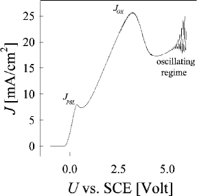
The solid - liquid junction of Silicon and HF - containing electrolytes exhibits a number of peculiar features, e.g. a very low density of surface states, i.e. an extremely well “passivated” interface [1]. If the junction is biased, the IV - characteristics (Fig. 3) in diluted HF is quite complicated and exhibits two current peaks and strong current- or voltage oscillations at large current densities (for reviews see [2, 3]). These oscillations have been decribed quantitatively by the Current-Burst-Model [4, 5, 6, 7].
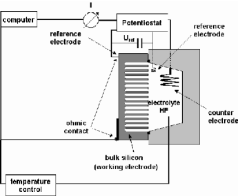
The PC controlled experimental setup is shown in Fig. 3. Using a four electrode arrangement, a potentiostat/galvanostat is contacting the sample and the electrolyte, allowing for a well defind potential resp. current for the electrochemical dissolution reactions. Backside contact, front- and/or backside illumination and electrolyte pumping can be varied as well as cell size (from under 0.3 cm up to wafers of 6 in), semiconductor material (Si, InP, GaAs, GaP) including various doping levels and crystallographic orientations. In addition, the electrolytes (e.g. HF, HCl, H2SO4) and their concentrations and temperature can be varied. With this setup a rich variety of porous semiconductors [8, 9] can be generated, from nanopores to mesopores and macropores, and with various regular and branching structures.
Most of the phenomenonology can be well understood within the framework of the Current-Burst-Model which seems to reflect a number of quite general properties of semiconductor electrochemistry.
2 The Current-Burst Model
The Current Burst Model [4, 5, 6, 10] states that the dissolution mainly takes place on small spots in short events, starting with a direct Si-dissolution, and possibly followed by an oxidizing reaction (see Fig. 3).
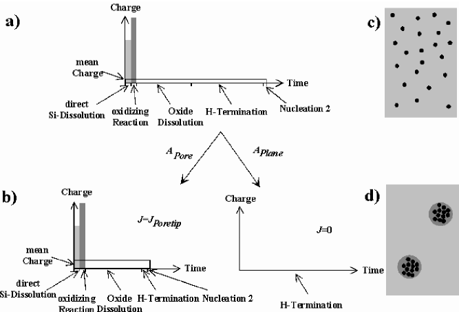
After these two short processes, the oxide hump undergoes dissolution, a time-consuming process which ensures at the location of the current burst a dead-time of fixed length during which no new burst can start. However, immediately after dissolution the Si surface has the highest reactivity, resulting in a maximal probability of annother current burst. Due to H-termination the surface becomes passivated, and the probability for bursts decays until it reaches the properties of a completely passivated Si surface, comparable to the situation before the nucleation of the first Current Burst.
2.0.1 Smoothing effect of Oxide Layers and global current oscillations
Depending on the regime in the IV-curve current bursts and their interaction play different roles: For extremely high currents, in the oscillation regime, one has a permanent oxide coverage, and due to the high forcing of the system Current Bursts are started at all locations where the oxide layer is sufficiently thin for a breakthrough. In this regime, a detailed Monte Carlo study [5, 6, 7] including the lateral interaction between CBs (overlap of the oxide humps of neighboring CBs) has shown that the CB Model quantitatively can explain the experimental observations of globally oscillating etching current. Due to a phase synchronization of neighboring CBs oxide domains are formed. The size of this domains increases with increasing oxide generation/reduced oxide dissolution. At a percolation point only one oxide domain exists on the sample surface with a synchronized cycle of oxide growth and dissolution, resulting in a macroscoping oscillation of the external current. The size of the domains as well as the oscillation time can be controlled by the chemical parameters. Even without global oscillations for all regions of the IV-curve where oxide is formed one finds domains of synchronized oxide growth which define the length scale for the roughness of the electrochemically polished sample surface and thus lead to a smoothing of the surface.
2.0.2 Passivation Effects: The Aging Concept
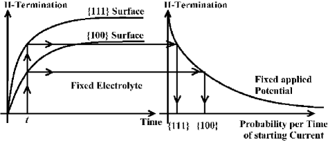
While at high current densities the semiconductor surface is completely covered with oxide, at low current densities most of the semiconductor surface will be in direct contact to the electrolyte. It is well known [1] that after chemical dissolution the free surface is passivated, i.e. the density of surface states reduces as a function of time which increases the stability of the surface against further electrochemical attack. Schematically the perfection of the surface passivation and the resulting reduction of the probability for a chemical attack as a function of time are plotted in Fig. 3. In silicon, the speed and the perfection of passivation of the (111) crystallographic surface is larger than for the (100) surface. This selective aging of surfaces leads to a self amplifying dissolution of (100) surfaces (which will become pore tips) and a preferential passivation of (111) surfaces (which will become pore walls). Under optimized chemical conditions with an extremely large passivation difference between (111) and (100) surfaces a self organized growth of octahedral cavities occurs. The octahedra consists of (111) pore walls. As soon as the complete surface of the octahedra reaches a critical value, it is easier to start a new cavity at a (100) tip of the old cavity, since the current density in the new, small cavity is larger and no surface passivation will occur until the surface again becomes to large. This growing mechanism leads to an oscillation of both the current through each pore and the diameter of each pore as a function of time. As in the case of oxide dissolution an internal time constant is related to the pore growth.
If a global current density smaller than the average current density in a current burst is applied, the aging concept becomes essential to explain the generation of macropores: At passivated surfaces, the nucleation probability of new current bursts is lower than at sites where a current burst has taken place before. Therefore the situation shown in Fig. 3(c) is much more unlikely than the situation in Fig. 3(d), so that the whole surface separates in two phases with current-carrying pores and passivated surface without contributions to the total current.
3 Consequences on Pore Geometries
As described above, depending on the electrochemical reactions the interaction of Current Bursts, either surface smoothing due to the dissolution of an isotropic oxide layer or strongly anisotropic dissolution of the semiconductor (due to the crystallography dependent aging of surfaces which is one of the most important reasons for pore formation) will dominate. Thus one obtains completely different surface morphologies when changing the electrochemical etching conditions; e.g. in a Si-HF-organic electrolyte system only by increasing the HF concentration (i.e. faster oxide dissolution and thus reduced influence of oxide) the electrochemical etching changes from electropolishing (strong oxide smoothing) over macropore formation (pores with diameters of several m and smooth pore walls) to mesopore formation (strongly anisotropic, narrow pores with diameters of less than 400nm) [11].
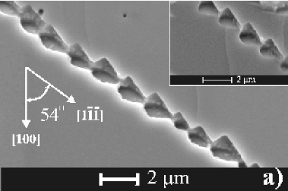
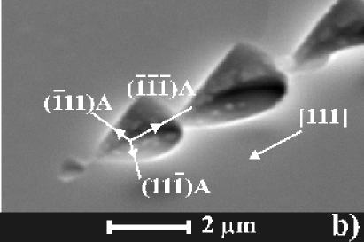
Silicon has one of the most stable oxides of all semiconductors. So generally electrochemical etching of III/V compounds leads to rougher surfaces and smaller pore diameters. In addition the surface aging of III-V compounds is more complicated, since there exist two different (111) surfaces; e.g. in GaAs only the A planes (Ga-rich planes) appear as stopping planes. So in most III-V compounds not octahedra (eight (111) surfaces as stopping planes) as in silicon are etched but tetrahedra with only four (111)A surfaces as stopping planes, and the B planes (As-rich) serve as preferential growing directions like the (100) directions in Si (Fig. 6).
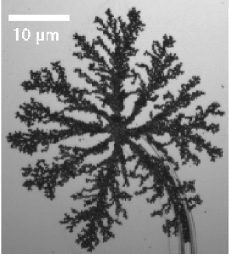
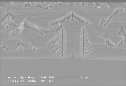
3.0.1 Lateral Growth of Current Bursts: Generation of Surface Fractals
For extremely low current densities and low HF concentration, the total number of active current bursts is so low that most of the surface is passivated or covered with oxide. CB nucleation becomes a severe problem. The neighborhood of a just terminated CB is therefore a preferential site for new CB nucleation, leading to the formation of surface fractals as shown in Fig. 6 (left). A further decrease of the current density allows for a partial passivation of the surface area of a terminated CB. According to Fig. 3 nucleation in the 100 direction of the surface near CBs will be preferential (Fig. 6).
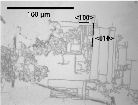
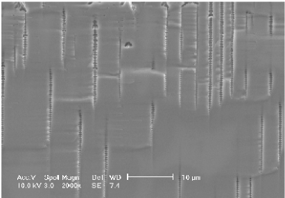
3.0.2 Sidebranching Pores and Suppression by Open-Loop-Control
For technical applications, it would be desirable to generate pores with a diameter of less than 500nm. However, at all etching conditions investigated up to now, in this diameter range always pores always show intensive side-branching. By modulation of the intensity of illumination or by modulation of the etching current with a modulation frequency meet the intrinsic time scale of the pore formation, the side pore formation is hindered by the reduction of the etching current at the right phase. (Fig. 6).
4 Conclusions
The Current Burst model, a local stochastic and highly nonlinear model, and the Aging concept describing the time- and orientation-dependence of the passivation behavior, provide on an intermediate level of abstraction a general approach to explain pore geometries, oscillations and synchronization with a minimum of material-dependent, but experimentally accessible, parameters. The lateral interaction of Current Bursts gives rise to synchronization phenomena, and a percolation transition to global ordering. Under special conditions lateral growth of fractal structures is obtained. An open-loop control can be successfully applied to suppress sidebranching of pores. To clarify quantitatively the dynamical processes in this system, further experimental and theoretical efforts have to be made.
References
- [1] E. Yablonovich, D.L Allara, C.C. Chang, T. Gmitter, T.B. Bright, Phys. Rev. Lett., 57, 249 (1986)
- [2] H. Föll, Appl. Phys. A 53, 8 (1991)
- [3] R.L. Smith, S. D. Collins, J. Appl. Phys., 71, R1 (1992)
- [4] J. Carstensen, M. Christophersen, H. Föll, Mat. Sci. Eng. B, 69, 23 (2000)
- [5] J. Carstensen, R. Prange, G. Popkirov, H. Föll, Appl. Phys. A 67, 459 (1998)
- [6] J. Carstensen, R. Prange, H. Föll, in: Proc ECS San Diego 1998, 98 148
- [7] J. Carstensen, R. Prange, H. Föll, J. Electrochem. Soc. 146(3), (1999) 1134
- [8] E. K. Propst, P.A. Kohl, J. Electrochem. Soc., 141, (1994) 1006
- [9] E. A. Ponomarev, C. Levy-Clement, J. Electrochem. Soc. Lett., 1, (1998) 1002
- [10] H. Föll, J. Carstensen, M. Christophersen, G. Hasse, in: Proc. ECS 2001
- [11] M. Christophersen, J. Carstensen, H. Föll, Phys. Stat. Sol. (a) 182, 45 (2000)