EL2–like defects in InP nanowires
Abstract
We have performed an ab initio total energy investigation, within the density functional theory (DFT), of antisite defects in InP nanowires (InPs) grown along the [111] direction. Our total energy results indicate that, (i) P antisites (PIn) are the most likely antisite defect compared with In antisites (InP), and (ii) the formation energies of P and In antisites do not depend on the diameter. In particular, thin InPs, diameters of 13 Å, the PIn antisite exhibits a trigonal symmetry, lying at 0.15 Å from the site, followed by a metastable configuration with PIn in an interstitial position (1.15 Å from the site). We find a PIn–P dissociation energy of 0.33 eV, and there is no EL2–like center for such a thin InP. However, EL2–like defects occur by increasing the diameter. For diameters of 18 Å, the PIn–P dissociation energy increases to 0.53 eV, which is 0.34 eV lower compared with the PIn–P dissociation energy for InP bulk phase, 0.87 eV. We mapped the atomic displacements and calculated the relaxation energy, Franck–Condon shift, upon single excitation of PIn induced states in InP. The formation (or not) of EL2–like defects, PIn–P dissociation energy barrier, and the Franck–Condon (FC) energy shift, can be tuned by the diameter.
pacs:
71.15.Mb, 71.15.Nc, 71.20.-bI Introduction
Antisite is one of the most studied native defect in III–V compounds, for instance, the EL2 center in GaAs. In a seminal work, Kamińska et al. Kamińska et al. (1985) established that the EL2 center exhibits a tetrahedral symmetry, formed by an isolated As antisite defect (AsGa). Afterward, several experimental von Bardeleben et al. (1986); Kabiraj and Ghosh (2005) as well as theoretical studies Chadi and Chang (1988); Dabrowski and Scheffler (1988); Zhang and Bernholc (1993); Chadi (2003); Overhof and Spaeth (2005) have been done aiming to clarify the structural and electronic properties of EL2 defect in GaAs. After more than ten year of investigations, currently there is a general agreement that the stable EL2 center is ruled by an isolated AsGa with symmetry, while the metastable EL2M structure is attributed to the AsGa atom displaced along the axis.
Its is well known that low temperature growth of other III–V semiconductors, not only GaAs, allows the preparation of highly nonstoichiometric compounds. Indeed, anion antisite defects in InP, PIn, has been identified for the first time unambiguously through the electron paramagnetic resonance technique by Kennedy and Wilsey Kenedy and Wilsey (1984). Dreszer et al. Dreszer et al. (1993), using Hall, high–pressure far–infrared absorption and optically detected magnetic resonance measurements (at low temperature), verified that InP has two dominant donor levels associated with the phosphorus antisite defect. Further investigations, based upon ab initio total energy calculations, proposed the formation of PIn antisites clusters in InP bulk Schmidt et al. (1999).
The most interesting property on this class of defects is the fact that they also exhibit a clear metastable behavior Chadi and Chang (1988); Mikucki et al. (2000); Caldas et al. (1990). A neutral anion–antisite defect in III–V compounds has a stable fourfold and a metastable threefold interstitial configuration, where the anion–antisite is displaced along the axis Caldas et al. (1990), similarly to EL2 and EL2M defects observed in GaAs. This center can be photo–excited into a metastable state, and from which it returns to the ground state by thermal activation. Thus, it is expected a persistent photoconductivity for PIn at low temperature.
Nowadays the electronic properties of several materials can be tailored throughout the manipulation/control of their size in the atomic scale. Within this new class of (nano)structured materials, the semiconductors nanowires (s) are attracting great deal of interest for future applications in several types of nanodevices. In particular, InP-nanowires (InPs) have been considered as a potential structure for fabrication of sensors, light emitting diodes, and field effect transistors Wang et al. (2001); Duan et al. (2001). Usually the vapor–liquid–solid mechanism, with a gold particle seed, has been utilized for the growth of these nanostructures Bhunia et al. (2003). These materials are quasi–one–dimensional with electrons confined perpendicularly to the growth direction. They exhibit interesting electronic and optical properties due to quantum confinement effects, viz.: the size dependence of InP bandgap Yu et al. (2003); Schmidt et al. (2005). Recent ab initio calculations, performed by Li et al. Li et al. (2005), suggested the formation of stable center in small GaAs quantum–dots, dot diameter smaller than 15 nm.
It is quite likely the formation of native defects during the growth process. Therefore, the structural and electronic properties of those defects are important issues to be addressed, in order to improve our understanding of native defects in quasi–1D semiconducting systems.
In this paper we carried out an ab initio total energy investigation of antisite defects in InPs. We find that the formation of EL2–like defects, antisite dissociation energy, and the Franck–Condon (FC) energy are ruled by the diameter. On the other hand, the antisite formation energies are insensitive to the diameter, being PIn antisites the most likely defect compared with InP. At the equilibrium geometry, the PIn atom in thin InP (diamenter of 13 Å) exhibits an energetically stable trigonal symmetry, followed by a metastable configuration with PIn in an interstitial position, 1.15 Å from the site. In this case, the PIn–P dissociation energy is 0.33 eV. Increasing the diameter (13 18 Å), we find a PIn–P dissociation energy of 0.53 eV, where PIn lying on the site represents the energetically most stable configuration. For the InP bulk phase, the PIn–P dissociation energy is equal to 0.87 eV. Similarly to the bulk phase, PIn in InP induces the formation of localized states within the energy bandgap. However, for such a thin system, this defect does not exhibit an EL2–like behavior. On the other hand, increasing the diameter, EL2–like defects are expected to occur. Finally, within a constrained density functional approach Artacho et al. (2004), we map the atomic displacements along thin InP upon single excitation of PIn induced states, and calculate the respective relaxation energy, “Franck-Condon” (FC) shift.
II Theoretical Approach
Our calculations were performed in the framework of the density functional theory (DFT) Hohenberg and Kohn (1964), within the generalized gradient approximation due to Perdew, Burke, and Ernzerhof Perdew et al. (1996). The electron–ion interaction was treated by using norm–conserving, ab initio, fully separable pseudopotentials Kleinman and Bylander (1982). The Kohn–Sham wave functions were expanded in a combination of pseudoatomic numerical orbitals Sankey and Niklewski (1989). Double zeta basis set including polarization functions (DZP) was employed to describe the valence electrons Artacho et al. (1999). The self–consistent total charge density was obtained by using the SIESTA code Soler et al. (2002). The InP was modeled within the supercell approach, where the InP bilayers were piled up along the [111] direction with periodicity length of and diameters of 13 and 18 Å ( represents the optimized lattice constant along the [111] direction of InP). The surface dangling bonds were saturated with hydrogen atoms. A mesh cutoff of 170 Ry was used for the reciprocal–space expansion of the total charge density, and the Brillouin zone was sampled by using one special k point. We have verified the convergence of our results with respect to the number and choice of the special k points. All atoms of the nanowire were fully relaxed within a force convergence criterion of 20 meV/Å.
III Results and Comments
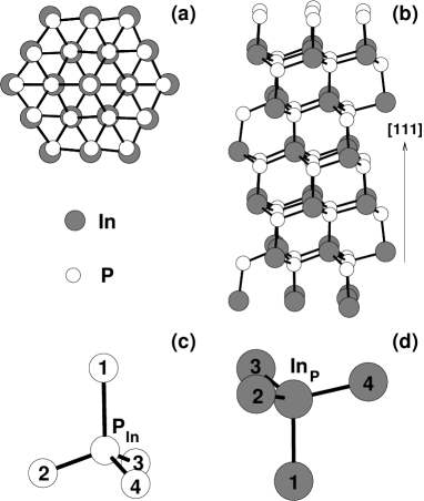
Figure 1 presents the atomic structure of thin InP, diameter of 13 Å, growth along the [111] direction, top view [Fig. 1(a)] and side view [Fig. 1(b)] (the hydrogen atoms are not shown). Due to the 1D quantum confinement, perpendicularly to the growth direction, the energy gap of InP increases compared with the bulk InP (1.0 eV) Schmidt et al. (2005). We find energy gaps of 2.8 and 2.2 eV for diameters of 13 and 18 Å, respectively. It is important to take into account those energy gaps are underestimated, with respect to the experimental measurements, within the DFT approach. Figure 2(a) presents electronic band structure of thin InP for wave vectors parallel to the [111] direction (L direction). At the point, the highest occupied states exhibit an energy split of 0.31 and 0.20 eV (), for diameter of 13 and 18 Å, respectively. The valence band maximum of bulk InP is described by a three–fold degenerated state. Such () energy splitting is due to the symmetry lowering of InP with respect to the bulk phase.

The energetic stability of antisites in InPs can be examined by the calculation of formation energies (). The formation energy of P and In antisites, PIn [Fig. 1(c)] and InP [Fig. 1(d)], respectively, can be written as,
We have considered the formation of antisites inner InPs. represents the total energy of InP with = PIn or InP antisite defect, and is the total energy of a perfect InP. () denotes the number of In (P) atoms in excess or in deficiency. The In and P chemical potentials, and , respectively, are constrained by following thermodynamic equilibrium condition, , where is the chemical potential of bulk InP. Under In rich (P poor) condition we will have , whereas under In poor (P rich) condition, Qian et al. (1988). For the heat of formation of bulk InP, , we have considered its experimental value, 0.92 eV.
Figure 3 presents our calculated results of for thin InP (diameter of 13 Å), as a function of the In chemical potential. It is clear that the formation of PIn is dominant compared with InP. This latter defect occurs only for In rich condition. At the In and P stoichiometric condition (dashed line in Fig. 3) we obtained = 2.15 eV and = 3.57 eV. Increasing the diameter (18 Å), we find = 2.18 eV. Within the same calculation procedure, we obtained similar formation energy results for the InP bulk phase, viz.: = 2.14 eV and = 3.59 eV. Those results indicates that, (i) there is an energetic preference of PIn antisites, compared with InP, for both structural phases of InP. (ii) The formation energy of does not depend on the diameter.

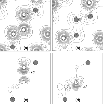
At the equilibrium geometry, PIn defect in bulk InP keeps the symmetry with PIn–P bond lengths of 2.49 Å, while InP exhibits a weak Jahn–Teller distortion along the [001] direction. Those results are in accordance with previous ab initio studies of antisites in InP Seitsonen et al. (1994); Schmidt et al. (1999); Castleton and Mirbt (2004). On the other hand, the equilibrium geometry of antisites in thin InP is quite different. The PIn–P1 bond, parallel to the growth direction, is stretched by 27% compared with the other three PIn–Pi bonds, in Fig. 1(c). Similarly for the InP antisites, InP–In1 is stretched by 8.6% compared with the other three InP–In bonds indicated in Fig. 1(d). Figures 4(a) and 4(b) depict the total charge densities along the PIn–P1 and InP–In1 bonds, respectively. In particular, due to the large PIn–P1 bond stretching, PIn is weakly bonded to P1, whereas the other PIn–P2, –P3 and –P4 bonds [see Fig. 4(a)] exhibit a strong covalent character. Therefore, different from bulk InP, PIn antisites in system exhibits a symmetry, with the PIn atom displaced from site by 0.15 Å along the [111] axis. Such a PIn displacement, along the axis, has not been observed by increasing the diameter to 18 Å. In this case, the PIn atom accupies a site and the PIn–P bond lengths are equal to 2.94 Å.
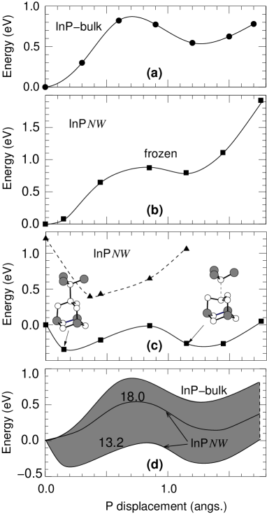
Several anion antisite defects in III–V materials were studied by Caldas et al. Caldas et al. (1990). In that work, based upon ab initio total energy calculations, the authors observed an energetically stable symmetry for PIn and a metastable configuration for the antisite atom displaced by 1.3 Å along the [111] direction. Indeed, in Fig. 5(a) we present our total energy results as a function of PIn displacement, along the [111] direction, for the InP bulk phase. We find that the symmetry represents the energetically most stable configuration, followed by an energy barrier of 0.87 eV at 0.7 Å from the site, z = 0.7 Å, breaking the PIn–P1 bond. Finally, the metastable configuration occurs for z = 1.2 Å, where the PIn occupies an interstitial site. Figures 5(b) and 5(c) present the energy barrier for PIn in thin InP. We have examined two different processes: (i) the In and P atoms of the are not allowed to relax during the PIn displacement [Fig. 5(b)]. (ii) The In and P coordinates are fully relaxed for each PIn step along the [111] direction, i.e. an adiabatic process [Fig. 5(c)]. It is noticeable that the energy barrier calculated in (i) is very similar to that obtained for PIn in bulk InP [Fig. 5(a)]. In (i) the energetically most stable configuration for PIn exhibits a symmetry, and we find a dissociation energy of 0.84 eV for z = 0.86 Å. Further PIn displacement indicates a metastable geometry for z 1.15 Å, where the PIn atom occupies an interstitial site. Meanwhile, in (ii) the symmetry, with the PIn atom lying at 0.15 Å from the site, represents the energetically most stable configuration. The PIn–P1 dissociation energy reduces to 0.33 eV (at z = 0.85 Å), and there is a metastable geometry for z 1.15 Å. The total energy difference between the stable () and the metastable () configurations, , in InP is equal to 0.084 eV, while in bulk InP we find = 0.53 eV. Comparing (i) and (ii) we verify that the atomic relaxation plays a fundamental rule not only to the energy barrier for the PIn atomic displacement along the [111] direction, but also for the equilibrium geometry of the PIn structure. Increasing the diameter, the energy barrier for PIn displacement will become similar to that obtained for bulk InP (an upper limit for very large diameter), see Fig. 5(d). Indeed, for diameter of 18 Å, we find a PIn–P1 dissociation energy of 0.53 eV, and equal to 0.14 eV. Those results indicate that the PIn–P1 dissociation barrier, and the total energy difference, can be tuned within the shaded region indicated in Fig. 5(d).
Focusing on the electronic structure, the formation of PIn defect in thin InP gives rise to a deep double donor state, labeled in Fig. 2(b), lying at 1.3 eV above . Such a PIn induced state is very localized within the fundamental band gap, being almost flat along the L direction. For PIn in bulk InP, ab initio studies performed by Seitsonen et al. Seitsonen et al. (1994) indicates the formation of an occupied state at 0.7 eV above the valence band maximum. The partial charge density contour plot of , Fig. 4(c), shows an anti-bonding orbital concentrated along the PIn–P1 bond. The lowest unoccupied state, , is also concentrated on the PIn antisite, as depicted in Fig. 4(d).
EL2 and EL2M centers in III–V are characterized by a stable and a metastable geometries for an isolated VIII interstitial atom. However, before the VIII antisite arrives to the metastable configuration, there is a strong electronic coupling between the highest occupied and the lowest unoccupied antisite induced states near to the local maximum for the VIII–V dissociation energy, see Fig. 3 in Ref. Caldas et al. (1990) and Fig. 4 in Ref. Dabrowski and Scheffler (1989).
Similarly, for thin InP, we examined the energy positions of single particle eigenvalues, and , as a function of the PIn displacement along the axis. Our calculated results, depicted in Fig. 6, reveal that there is no electronic coupling between and . Thus, based upon the calculated energy barrier [Fig. 5(c)], and the evolution of the antisite induced states, and , we can state that there is no EL2–like center in thin InPs. On the other hand, increasing the diameter [Fig. 5(d)], EL2–like center is expected to occur in InP.

Within the DFT approach, we have examined the structural relaxations upon single excitation from the highest occupied state () to the lowest unoccupied state () of PIn in thin InP. We have used the calculation procedure proposed by Artacho et al., where the single excitation was modeled by “promoting an electron from the highest occupied molecular orbital (HOMO) to the lowest unoccupied molecular orbital (LUMO)”Artacho et al. (2004), i.e. a “constrained” DFT calculation. So that, promoting one electron from to , , we obtained the equilibrium geometry (full relaxations) as well as the self–consistent electronic charge density. The atomic relaxations along thin InP, upon single excitation, are localized near to the PIn position. Since we are removing one electron from the anti-bonding orbital depicted in Fig. 4(c), the PIn–P1 bond shrinks by 0.12 Å (2.90 2.78 Å), and there is radial a contraction of 0.2 Å at z = 6.8 Å.
The structural relaxations are proportional to the degradation of optical energy due to the atomic displacements associated with such a single excitation, FC shift. Comparing the radial and the longitudinal displacements, we verify that the most of the FC shift comes from the atomic relaxation parallel to the growth direction. The atomic displacements along the radial direction () are localized nearby PIn, lying within an interval of Å. While the atomic displacements parallel to the growth direction () lie within a range of Å, being less concentrated around the PIn antisite position. We find a FC energy shift of 0.8 eV, which is quite large compared with the InP bulk phase. Within the same calculation approach, we find a FC energy shift of 0.05 eV for InP bulk. Previous ab initio study indicates a FC energy shift of 0.1 eV for bulk InP. Thus, suggesting that the FC energy shift also can be tuned by controlling the diameter.
IV Conclusions
In summary, we have performed an ab initio total energy investigation of antisites in InP. We find that the PIn antisite is the most likely to occur. For thin InPs the PIn atom exhibits a trigonal symmetry, followed by a metastable P interstitial configuration. Increasing the diameter (18 Å), PIn occupying the site becomes the energetically most stable configuration. The calculated energy barrier, for PIn displacement along the axis, indicates that there is no EL2–like defect in thin InPs. However, increasing the diameter, 13 18 Å, we observe the formation of EL2–like defects in InP. Within a “constrained” DFT approach, we calculated the structural relaxations and the FC energy shift upon single excitation of the electronic states induced by PIn. We inferred that not only the formation (or not) of EL2–like defects, but also (i) the PIn–P dissociation energy, (ii) the total energy difference between stable and metastable PIn configurations, , and the (iii) FC energy shift can be tuned by controlling the InP diameter.
Acknowledgments
The authors acknowledge financial support from the Brazilian agencies CNPq, FAPEMIG, and FAPESP. The most of calculations were performed using the computational facilities of the Centro Nacional de Processamento de Alto Desempenho/CENAPAD-Campinas.
References
- Kamińska et al. (1985) M. Kamińska, M. Skowroński, and W. Kuszko, Phys. Rev. Lett. 55, 2204 (1985).
- von Bardeleben et al. (1986) H. J. von Bardeleben, D. Stiévenard, D. Deresmes, A. Huber, and J. C. Bourgoin, Phys. Rev. B 34, 7192 (1986).
- Kabiraj and Ghosh (2005) D. Kabiraj and S. Ghosh, Appl. Phys. Lett. 87, 252118 (2005).
- Chadi and Chang (1988) D. J. Chadi and K. J. Chang, Phys. Rev. Lett. 60, 2187 (1988).
- Dabrowski and Scheffler (1988) J. Dabrowski and M. Scheffler, Phys. Rev. Lett. 60, 2183 (1988).
- Zhang and Bernholc (1993) Q.-M. Zhang and J. Bernholc, Phys. Rev. B 47, 1667 (1993).
- Chadi (2003) D. J. Chadi, Phys. Rev. B 68, 193204 (2003).
- Overhof and Spaeth (2005) H. Overhof and J.-M. Spaeth, Phys. Rev. B 72, 115205 (2005).
- Kenedy and Wilsey (1984) T. Kenedy and N. Wilsey, Appl. Phys. Lett. 44, 1089 (1984).
- Dreszer et al. (1993) P. Dreszer, W. M. Chen, K. Seendripu, J. A. Wolk, W. Walukiewicz, B. W. Liang, C. W. Tu, and E. R. Weber, Phys. Rev. B 47, 4111 (1993).
- Schmidt et al. (1999) T. Schmidt, R. Miwa, A. Fazzio, and R. Mota, Phys. Rev. B 60, 16475 (1999).
- Mikucki et al. (2000) J. Mikucki, M. Baj, D. Wasik, W. Walukiewicz, W. G. Bi, and C. W. Tu, Phys. Rev. B 61, 7199 (2000).
- Caldas et al. (1990) M. J. Caldas, J. Dabrowski, A. Fazzio, and M. Scheffler, Phys. Rev. Lett. 65, 2046 (1990).
- Wang et al. (2001) J. Wang, M. S. Gudiksen, X. Duan, Y. Cui, and C. M. Lieber, Science 293, 1455 (2001).
- Duan et al. (2001) X. Duan, Y. Huang, Y. Cui, J. Wang, and C. M. Lieber, Nature 409, 66 (2001).
- Bhunia et al. (2003) S. Bhunia, T. Kawamura, Y. Watanabe, S. Fujikawa, and K. Tokushima, Appl. Phys. Lett. 83, 3371 (2003).
- Yu et al. (2003) H. Yu, J. Li, L. Richard A, L.-W. Wang, and W. Buhro, Nat. Mater. 2, 517 (2003).
- Schmidt et al. (2005) T. M. Schmidt, R. H. Miwa, P. Venezuela, and A. Fazzio, Phys. Rev. B 72, 193404 (2005).
- Li et al. (2005) J. Li, S.-H. Wei, and L.-W. Wang, Phys. Rev. Lett. 94, 185501 (2005).
- Artacho et al. (2004) E. Artacho, M. Rohlfing, M. Côté, P. D. Haynes, R. J. Needs, and C. Molteni, Phys. Rev. Lett. 93, 116401 (2004).
- Hohenberg and Kohn (1964) P. Hohenberg and W. Kohn, Phys. Rev. 136, B864 (1964).
- Perdew et al. (1996) J. P. Perdew, K. Burke, and M. Ernzerhof, Phys. Rev. Lett. 77, 3865 (1996).
- Kleinman and Bylander (1982) L. Kleinman and D. M. Bylander, Phys. Rev. Lett. 48, 1425 (1982).
- Sankey and Niklewski (1989) O. F. Sankey and D. J. Niklewski, Phys. Rev. B 40, 3979 (1989).
- Artacho et al. (1999) E. Artacho, D. Sánchez-Portal, P. Ordejón, A. Garcia, and J. M. Soler, Status Solid B 215, 809 (1999).
- Soler et al. (2002) J. M. Soler, E. Artacho, J. D. Gale, A. García, J. Junquera, P. Ordejón, and D. Sánchez-Portal, J. Phys.: Condens. Matter 14, 2745 (2002).
- Qian et al. (1988) G.-X. Qian, R. M. Martin, and D. J. Chadi, Phys. Rev. B 38, 7649 (1988).
- Seitsonen et al. (1994) A. P. Seitsonen, R. Virkkunen, M. J. Puska, and R. M. Nieminen, Phys. Rev. B 49, 5253 (1994).
- Castleton and Mirbt (2004) C. W. M. Castleton and S. Mirbt, Phys. Rev. B 70, 195202 (2004).
- Dabrowski and Scheffler (1989) J. Dabrowski and M. Scheffler, Phys. Rev. B 40, 10391 (1989).