Influence of chopped laser light onto the electronic transport through atomic-sized contacts
Abstract
This article reports on the influence of laser
irradiation onto the electrical conductance of gold nanocontacts
established with the mechanically controllable breakjunction
technique (MCB). We concentrate here on the study of reversible
conductance changes which can be as high as 200%. We investigate
the dependence on the initial conductance of the contacts, the
wavelength, the intensity and position of the laser spot with
respect to the sample. Under most conditions an enhancement of the
conductance is observed. We discuss several physical mechanisms
which might contribute to the observed effect including thermal
expansion, rectification and photon-assisted transport. We
conclude that thermal expansion is not the dominating one.
Corresponding author: Elke Scheer (elke.scheer@uni-konstanz.de)
pacs:
73.63.Rt, 85.65.+h, 73.50.PzI Introduction
Metallic nanostructures with fine tips and sharp edges are interesting candidates for optical antennae due to possible field enhancement (FE) effects at the parts with small curvatures and narrow gaps. The excitation of resonant plasmons can amplify the electrical field at positions within or close to the nanostructures. The field enhancement in bow-tie shaped metal structures has so far been calculated and detected by several near field optical methods Mühlschlegel et al. (2005) and direct imaging via ablation of the underlying substrate leidererapl . Here we address the question whether FE can be detected in the electronic transport between two metallic tips connected via an atomic-size contact. The central part of the device resembles a bow-tie Faharani et al. (2005). For this geometry to our knowledge no calculations of the magnitude of the FE do exist, however, it can be assumed that as long as the coupling between the two electrodes is weak, it should still exist. Such contacts can be realized via mechanically controllable breakjunctions (MCBs), i.e. free-standing nanobridges with lateral sizes in the order of 100 nm and bridge lengths of several micrometers, which have been fabricated on a flexible substrate. By bending the substrate the bridge is elongated and its cross-section is reduced until it finally breaks at some position. Just before it breaks the constriction forms a contact with one or a few atoms in cross section.
These contacts represent model systems which are regularly used for revealing and understanding the electronic transport properties of atomic scale circuits agrait03 (Agraït et al. (2003). In this limit the electronic transport can be attributed to a small number of independent electronic modes, nick-named ”conduction channels” Landauer (1970). The transport properties are fully described by a set of transmission coefficients which depends both on the chemical properties of the atoms forming the contact and on their geometrical arrangement Scheer et al. (1997, 1998). The conductance of such a contact is given by the Landauer formula: , where is the conductance quantum.
Besides this aspect, MCBs can be broken to form electrode pairs with a narrow gap in the order of picometers to nanometers between two very fine metallic tips. Such electrodes are used for contacting individual nanoobjects such as clusters or molecules Cuniberti et al. (2005); Reichert et al. (2002); Böhler et al. (2004). Here we address the question whether the MCB electrodes are suitable optical antennae as well. Contrary to planar electrode pairs on a substrate, the MCB electrodes provide the possibility to rearrange the geometry of the device and therewith the FE effects in the constriction. By breaking the nanobridge to separate electrodes one reduces the interaction between the electrodes, but for small distances it is still possible to measure the tunneling current. In particular, in the so-called contact regime the interaction between the tips has to be taken into account for understanding the optical properties. The electronic transport is in the quantum regime described above.
Due to the electronic structure of molecules with well defined gaps between the individual molecular orbitals the current-voltage characteristics (IVs) of single-molecule devices are strongly nonlinear Reichert et al. (2002). Under certain conditions the irradiation with laser light can be regarded as the addition of an ac-electrical field to the dc voltage used for the transport measurement. In this situation rectification of the current and the creation of asymmetries in the IVs is expected Möller et al. (1991). Furthermore, by irradiation with laser light with a suitable frequency photochromic molecules may undergo conformational changes which may be reflected in the electronic transport properties. Dulić et al. observed a switching from the ”on” , i.e. low resistance state of a molecular contact to the ”off” state by shining light with a frequency which is known to create a conformation change when the molecules are in solution or deposited in an ensemble on a surface Dulić et al. (2003). However, the switching from ”off” to ”on” was not observed. The interpretation of those resistance changes is hampered by the fact that several explanations are possible for the observation of a strong resistance increase, among which the breaking of the contact due to geometry of the electrodes is one of the most likely scenarios.
In our work we therefore concentrate on the study of laser illumination onto the metal electrodes alone. Already for this conceptually rather simple device the influence of the laser light may be manifold. One rather trivial effect is the geometry change of the tips due to thermal expansion because of the deposited energy of the laser pulse. This effect has been shown to be the dominating one for a scanning tunneling microscope (STM) under pulsed laser light irradiation Boneberg et al. (1998); Grafström et al. (1998). However, for the MCB geometry this effect is expected to be much smaller due to the very small dimensions of the freestanding bridge arms.
The electromagnetic wave of the laser pulse represents a high-frequency electrical field that is coupled to the metal bridge. The ac field may create an asymmetric contribution to the dc current for those voltages where the IVs are nonlinear Möller et al. (1991). Asymmetric irradiation of the contact might create temperature gradients - and thus thermo-currents - , or photocurrents. Last but not least, photon assisted transport (PAT), i.e. the creation of quasiparticles with an energy above the Fermi energy will create a nonequilibrium in the electronic system. This means that high-energetic quasiparticles may contribute to the transport. Due to the energy dependence of the transmission coefficients of the conduction channels the resistance of the contact will change Viljas&Cuevas (2006a).
We will discuss these mechanisms in the light of our experimental results and come to the conclusion that besides thermal expansion at least one additional mechanism is active.
II Experimental
II.1 MCB technique and fabrication of lithographic breakjunctions
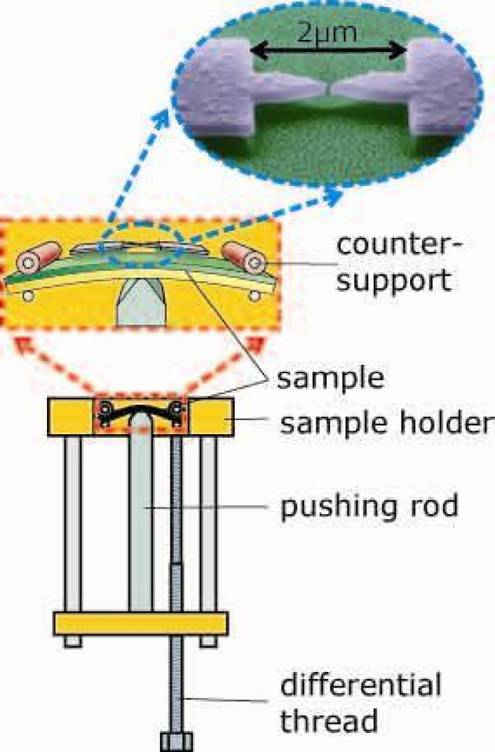
The nanoelectrodes are arranged by the mechanically controllable breakjunction (MCB) technique agrait03 (Agraït et al. (2003). MCBs consist of a freestanding micro- or nanobridge on a flexible substrate embedded in an electrical circuit by leads which are in rigid contact with the substrate (see Fig. 1). By bending the substrate with the help of a mechanical or piezo drive the freestanding parts are elongated and constricted. The dimensions can be chosen such that constrictions with lateral dimensions of a single or few atoms or vacuum tunnel contacts between two atomically sharp tips can be arranged and stabilized. The main advantage of the MCB technique compared to atomic size contacts arranged with STMs is the built-in stability due to the high reduction ratio (between the motion of the pushing rod and the displacement of the bridge arms). Mechanical vibrations are damped with a factor which enables MCBs to be used without external vibration damping even when mounted in vacuum chambers with mechanical pumps. Different realizations of this technique have been developed, among which the lithographic MCBs that we apply here offer the possibility to use a purely mechanical drive and to incorporate the device into more complex electronic circuits.
The samples are fabricated by electron beam lithography along the lines of Ref. van Ruitenbeek et al. , 1996. The suspended nanobridges are 2 m long and 100 nm thick made of Au with a constriction in the center (cf. insert of Fig. 1). The thickness of the flexible steel substrates is mm, the distance between the counter-supports of the bending mechanism is 19 mm. The metallic substrate is covered with a 2 m thick polyimide layer which serves for planarization, electrical isolation and as sacrificial layer for suspending the central part of the sample. The bridge is underetched in an isotropic oxygen plasma which reduces the height of the polyimide layer by about 500 to 1000 nm. At the narrow constriction the nanobridge is now unsupported. The resistance of the nanobridge does not increase during the etching process, indicating that the reaction between the oxygen ions and Au is weak.
The samples are then mounted on a three-point bending mechanism as shown in Fig. 1. A differential screw with 100 m pitch, driven by a dc-motor and an (exchangeable) reduction gear box, controls the motion of the pushing rod that bends the substrate. With these sample parameters we achieve reduction ratios of the order of 30000:1. The relative displacement of the pushing rod can be controlled to a precision of nm, which thus results in a relative motion of the two anchor points of the bridge of around 1 pm. This was verified using the exponential dependence of the conductance on the inter-electrode distance in the tunnel regime.
Typical opening speeds for the continuous measurements (see below) are 215 nm/s for the pushing rod, corresponding to a displacement of the bridge-anchor points of 7 pm/s, much slower than typical opening speeds of nanocontacts fabricated with the help of a STM or the ”notched-wire” breakjunction technique agrait03 (Agraït et al. (2003). This limitation in opening speed, however, limits the number of opening traces that can be recorded within a reasonable time.
The mechanics are designed such that the position of the nanobridge remains constant upon bending the substrate in order to ensure stable optical focal conditions (see below). The MCB setup is operational at ambient conditions as well as in vacuum and or at low temperatures. The measurements presented in this article have been performed under UHV conditions at room temperature on three nominally identical samples.
II.2 Optical setup
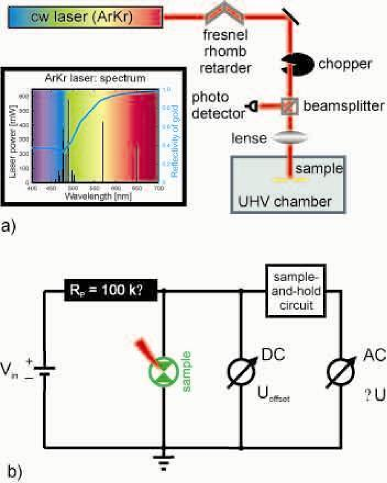
The optical setup is depicted in Fig. 2 a. We use an Argon-Krypton continuous wave (cw) laser system as light source, which allows us to select one of several wavelengths in the range between 480 nm and 650 nm. The cw laser beam is fed through a - Fresnel rhomb retarder in order to tilt the polarization angle, and is afterwards chopped to produce light pulses with a length of 700 s and a repetition rate of 50 Hz. A beam-splitter in the optical path divides the chopped light. One part is reflected into a photo detector to create a trigger event, the other part is focussed onto the sample by a lens. The beam spot on the sample has a diameter of about 20 to 25m, depending on the wavelength.
The sample is mounted on the breaking mechanism inside a UHV chamber with a base pressure of 10-9 mbar in order to avoid contamination of the breakjunction. The UHV chamber is equipped with a fused silica-window to minimize the change of polarization of the laser light due to stress birefringence. If not stated differently, the polarization was chosen parallel to the current for the measurements presented here. For perpendicular polarization similar results but with an amplitude that is smaller by about a factor 2 to 3 are observed. A more detailed investigation is necessary in order to quantify the exact influence of the polarization.
II.3 Electronic circuit
The sample is connected with a 100 k series resistor to a dc-voltage source (Fig. 2 b). This resistor is required to protect the sample against high-voltage spikes created e.g. by electrostatic discharges. The combination with the sample builds a voltage divider. Thus, we have the possibility to calculate the conductance of the sample from the measured voltage across it.
Because of the different voltage ranges of the dc-voltage signal
(without light) and the small voltage variation due to the
light-induced-signal (LIS) during the pulse, it is
necessary to measure the signal across the sample in dc- as well
as in ac-mode in order to get a good resolution in both parts. The
amplitude of the ac-part, caused by each light pulse, is measured
by a sample-and-hold circuit (S/H) with an integrating amplifier.
The acquired amplitude is held and displayed over the whole
chopping period, until the next light pulse appears. Thereafter
the next voltage variation is measured by the (S/H)
circuit and held again.
To calculate the conductance variation caused by the incident
light, we convert the dc-voltage and the sum of the dc- and
ac-signal (accounting for the amplification of the (S/H) circuit)
into conductance and compare the values. The time resolution of
the experiment is limited by the fact that the chopper is located
at a position where the laser spot is rather large. Thus, the
laser intensity rises and drops on a time scale of 100 s. The
response time of LIS is similar demonstrating a roughly linear
intensity dependence of the LIS (see inset of Fig. 3).
II.4 Control experiments
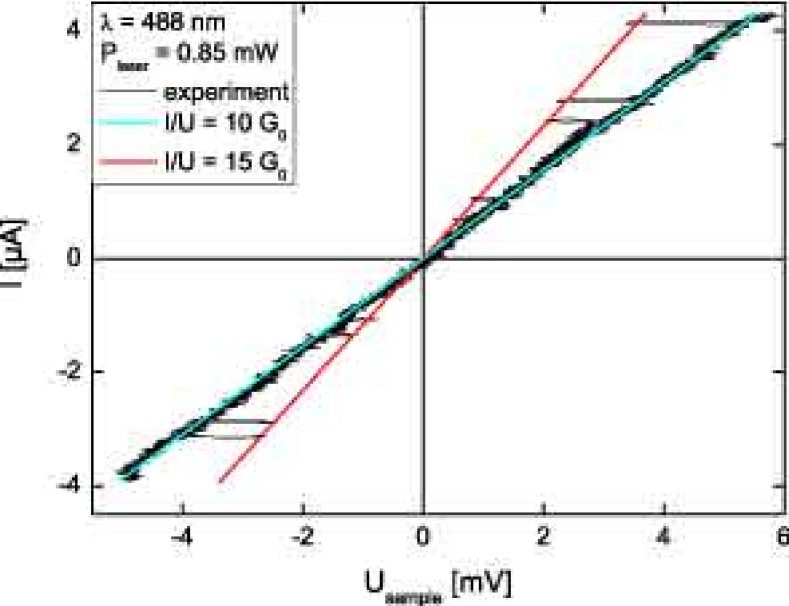
Figure 4 shows a current-voltage characteristic (IV) of a contact for a conductance without irradiation of , as indicated by the blue line. At several current values laser pulses with duration s, nm and power mW are shed onto the contact. During the pulse the absolute value of the voltage measured across the contact is reduced by the same amount for both polarities. The amplitude of the laser induced voltage drop is proportional to the current. Neither current nor voltage offsets nor asymmetries are observed, indicating that the effect of the light is a bare change of conductance to as indicated by the red line. The fact that the conductance change is observed for linear IVs indicates that it is not created by a rectification effect as observed in Ref. Möller et al. , 1991.
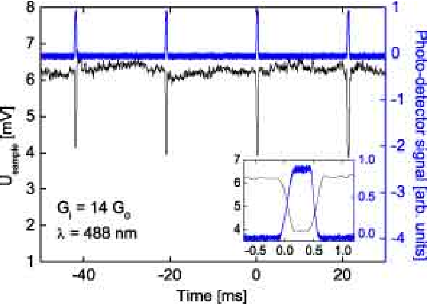
The conductance change is completely reversible and reproducible for a given contact as demonstrated by shining repeated pulses onto the bridge (see Fig. 3); only changes upon variation of the contact geometry. However, continuous irradiation of the device with nm for several seconds with a similar power ( mW) results in irreversible conductance changes (not shown), indicating that irreversible atomic rearrangements are triggered by the cw light.
III Results and discussion
When elongating the bridge without irradiation, its conductance decreases in steps of the order of 1 , their exact sequence changing from opening to opening because the atomic arrangement of the central region differs for each opening process. The typical distance scale for a conductance change of is the lattice constant, i.e. a few tenths of a nm. Because of the individual rearrangements it is difficult to draw conclusions from the behavior of individual contacts or openings. Experiments on a large ensemble of metallic contacts have demonstrated the statistical tendency of atomic-size contacts to adopt element-specific preferred values of conductance. The actual preferred values depend not only on the metal under investigation but also on the experimental conditions. However, for many metals, and in particular monovalent metals like Au, the smallest contacts have a conductance close to (Ref. agrait03, Agraït et al. (2003).
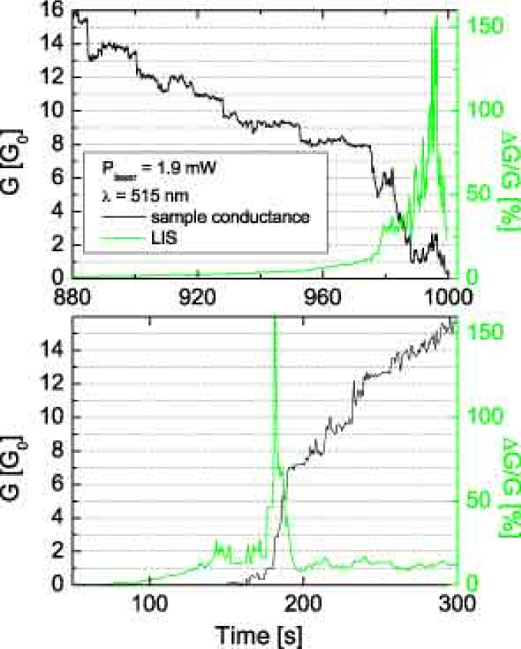
Also the LIS varies from contact to contact. Therefore, in order to deduce the typical behavior, we simultaneously measure the conductance and the LIS upon continuously opening and closing the bridge. Fig. 5 gives an example of such measurements recorded for green light with nm. The conductance plateaus are not always very well marked. The tunneling regime is difficult to assess when opening because the contact tip atoms relax back upon breaking giving rise to strong decrease in the conductance by several orders of magnitude agrait03 (Agraït et al. (2003). When closing the contact again, very often the first contact after the ”jump to contact” has already a conductance of several . The LIS is positive throughout the whole opening process. In some occasions it adopts small negative values in the tunneling regime (not shown in this example). It reaches a maximum with large fluctuations for . From these observations we shall draw the important conclusion that thermal expansion alone cannot explain the LIS. In similar experiments but using an STM instead of a MCB, it has been shown that thermal expansion is the most important mechanism giving rise to conductance changes Boneberg et al. (1998); Grafström et al. (1998).
A priori it is not predictable whether in our geometry thermal expansion should give rise to an enhancement or a reduction of the conductance, since the laser spot also hits the underlying substrate. If the thermal expansion of the nanobridge is larger than the one of the substrate, the two electrodes are pushed together, if the thermal expansion of the substrate exceeds the one of the nanobridge, then the two tips are pulled apart from each other. Whether the motion of the tips results in an enhancement or reduction of depends on the plateau shape of the conductance trace upon opening: For a horizontal plateau the conductance is constant upon stretching the contact, i.e. changing the bridge length does not give any conductance change. For negatively declined plateaus, i.e. decreasing upon stretching, an elongation of the tips yields an enhancement of while positively declined plateaus give rise to a decreasing when pushing the tips together. The conductance trace of Fig. 5 shows horizontal as well as negatively and (only rarely) positively declined plateaus. Nevertheless, in our experiments the LIS is almost always found to be positive (see below). Furthermore, the strong exponential distance dependence of for vacuum tunneling should give rise to a large relative conductance change upon irradiation. However, our observed LIS is usually smallest in this regime. In Fig. 5 we chose an example where it is particularly large and of comparable size with the signal for large contacts. Hence, although thermal expansion is very likely to be present in our experiment, it is expected not to be the dominating effect for the LIS.
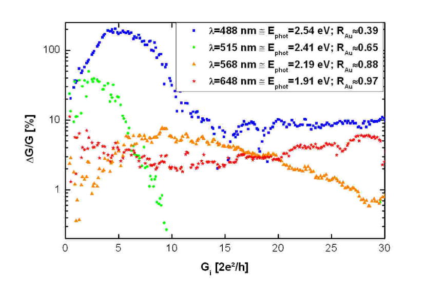
In order to further elucidate the origin of the effect, we performed statistical investigations of the LIS for different light wavelengths. Fig. 6 depicts histograms of the relative conductance changes recorded on the same sample with similar laser power for four wavelengths and from analyzing between 35 and 170 opening traces each. The histograms are calculated as follows: For each opening trace the LIS is related to the initial conductance value without laser irradiation for which it was measured. The average LIS and its standard deviation are then plotted on a logarithmic scale versus .
As seen from Fig. 6 the signal is largest for blue light with nm and decreases with increasing wavelength. The LIS also depends on the conductance: it is largest for few-atom contacts and decreases for smaller and larger contacts. The value for which the maximum signal is observed does not depend systematically on . Although for certain opening traces the LIS is negative in the tunnel regime, the average values plotted here are positive.
The amplitude dependence of the LIS on correlates with the variation of the reflectivity of gold with the wavelength, which increases from 39% for the blue light up to 97% for the red light. This means that the deposited energy decreases by a factor of , while the maximum signal size decreases by about a factor of 40. The additional suppression of the LIS in the red is in accordance with the predictions of photo assisted transport Viljas&Cuevas (2006a) (see below.)
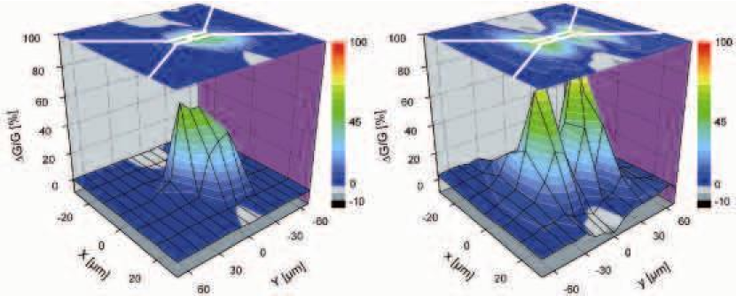
Further information about the effect is obtained from recording a map of the signal size with respect to the position of the laser spot. The maps for blue and red light for an average conductance of and polarization perpendicular to the transport direction are shown in Fig. 7. The laser spot with a diameter of m is much larger than the bridge length, therefore the step size for the map is set to m. A clear position dependence is observable for all wavelengths. In Fig. 7 we superimposed a drawing of the sample geometry with the recorded LIS. The largest signal is observed when the center of the laser spot is located on the leads within a distance of m from the contact. It is symmetrical with respect to the contact. For red light a relative minimum is observed right at the position of the contact, while for blue light the signal is almost constant along the bridge. More than a diameter of the laser spot aside of the contact a small negative LIS is observed for the red light.
These observations can tentatively be explained as follows: The
negative signal when mainly irradiating the substrate indicates
that the effect of thermal expansion of the substrate tends to
decrease the conductance. Thus, the observed enhancement when the
laser spot does touch the metallic bridge, is due to light coupled
into the metallic bridge.
When irradiating the narrow constriction, only a small part of the
laser energy is coupled into the metallic bridge, but the
majority is absorbed by the substrate. Thus the minimum in the
LIS can be explained by the geometry of the experiment. Contrary,
the lack of minimum for the blue light although the geometry of the experiment is the same
indicates that an energy dependent mechanism is at the origin of
the strong enhancement.
A possible explanation could be photon assisted transport reflecting the energy dependence of the transmission coefficients of the conduction channels as proposed by Viljas and Cuevas Viljas&Cuevas (2006a). The mechanism is such that the incoming photons are absorbed by individual electrons, creating quasiparticles with energy below and above the respective Fermi energies of both electrodes. Since electrons on both sides of the constriction are concerned, the quasiparticles may travel in both directions. The transmission coefficients of the conduction channels reflect the local density of states at the central atom. Although the exact functional dependence of the transmission differs from that of the density of states, the typical energy scales are identical. For single-atom contacts of Au it has been predicted that the typical energy scale for non-negligible variation of the transmission coefficients is about one to several electron volts Cuevas et al. (1998). Those quasiparticles have a lifetime in the order of several ten femtoseconds, depending on their energy Cao et al. (1998). It has been shown that the effective thermalization times are much longer than the lifetimes estimated from Fermi liquid theory Guo et al. (2001); Aeschlimann et al. (2000); Cao et al. (1998). Since furthermore the transport mode of the highly excited quasiparticles differs from the thermal ones close to the Fermi edge, it is difficult to determine a corresponding range or scattering length Cao et al. (1998). A rather optimistic estimate yields a length in the order of a few hundred nanometers. This means that only incoming photons within this distance from the contact are able to create the high-energetic quasiparticles which give rise to the conductance change. For photon energies of a few eV, strong variations of the conductance are thus expected, the sign of which is not easy to predict because of the particular energy landscape of gold atomic-size contacts Viljas&Cuevas (2006b). The dominating transmission of the s-band decreases for smaller as well as for higher energies, but for lower energies the 5d-bands and for higher energies the 6p-bands start to contribute to the transport. Since no detailed calculation for gold does exist by now, a quantitative analysis in terms of PAT is not possible yet.
Because of the short lifetime of the high energetic quasiparticles one would thus expect to have a maximal signal closest to the contact, but because of the reduced lateral size less photons arrive at the metal bridge. For blue light the increase of the efficiency onto the transport and the loss in number of photons seem to compensate while for red photons the loss in number dominates. We speculate that the influence of the red light with photon energy below the plasma edge and blue light above it might be of different nature. Below eV (see Ref. Simmons&Potter , 2000) corresponding to nm a hot electron sea might be created which distributes the energy among the plasma electrons, while above the energy transfer to individual electrons is more likely. Furthermore, the strong energy dependence of the lifetime yields considerably shorter lifetimes for blue than for red light. Further experiments are necessary to verify this interpretation. Nevertheless we would like to mention that the observed wavelength dependence and amplitude of the signal are in accordance with this mechanism.
Taking into account the geometry of the sample, the focal cross-section, the intensity of the laser, pulse length, and the reflectivity at a given wavelength we obtain a rough estimate for the number of created high-energy quasiparticles per photon. For nm and the contact shown in Fig. 3 at an applied voltage of 1 mV this value is .
IV Summary
We have presented electric transport measurements carried out on atomic-size contacts connecting the two parts of a bow-tie shaped optical-antenna geometry under irradiation with laser light. We observe strong conductance enhancements, the amplitude of which strongly depends on the wavelength of the laser. We discuss several possible mechanisms and come to the conclusion that besides thermal expansion photon-assisted transport is most likely at the origin of our observations.
V Acknowledgements
Fruitful discussions with J.C. Cuevas, J.K. Viljas and A. Leitenstorfer are gratefully acknowledged. This work was financially supported by the Deutsche Forschungsgemeinschaft through SFB 513 and the Alfried Krupp von Bohlen und Halbach-Stiftung.
References
- Aeschlimann et al. (2000) Aeschlimann, M., Bauer, M., Pawlik., S., Knorren, R., Bouzerar, G., Bennemann, K. H. (2000) Transport and dynamics of optically excited electrons in metals, Appl. Phys. A 71, 485-491
- (2) Agraït, N., Levy Yeyati, A., van Ruitenbeek, J.M. (2003) Transport properties of atomic-size conductors, Phys. Rep. 377, 81-279
- Böhler et al. (2004) Böhler, T. , Grebing, J., Mayer-Gindner, A., v. Löhneysen, H., Scheer, E. (2004) Mechanically controllable break junctions in use as electrodes in molecular electronics Nanotechnology 15, S465-S471
- Boneberg et al. (1998) Boneberg, J., Tresp, M., Ochmann, M., Münzer, H.-J., Leiderer, P. (1998) Time-resolved measurements of a STM-tip upon illumination with a nanosecond pulse, Appl. Phys. A 66, 615-619; Boneberg, J., Münzer H.-J., Tresp, M., Ochmann, M., Leiderer, P. (1998) The mechanism of nanostructuring upon nanosecond laser irradiation of a STM-tip, Appl. Phys. A 67, 381-384
- Cao et al. (1998) Cao, J., Gao, Y., Elsayed-Ali, H. E., Miller, R.J. D., Mantell, D. A. (1998) Femtosecond photoemission study of ultrafast electron dynamics in single-crystal Au(111) films, Phys. Rev. B 58, 10948-10952
- Cuevas et al. (1998) Cuevas, J. C., Levy Yeyati, A., Martín-Rodero, A., Rubio Bollinger, G., Untiedt, C., Agraït, N. (1998) Evolution of conducting channels in metallic atomic contacts under elastic deformation, Phys. Rev. Lett. 81, 2990-2993
- Cuniberti et al. (2005) Cuniberti, G., Fargas, G., Richter, K. (2005) Introducing Molecular Electronics, Lecture Notes in Physics, Springer-Verlag, Berlin
- Dantscher et al. (2006) Dantscher, S., Kennerknecht, C., Schramm, S., Pfeiffer, W., Würfel, J. U., Elbing, M., Mayor, M., Weber, H. B., Photocurrents in nanoscale tunnel junctions and single-molecule contacts, preprint
- Dulić et al. (2003) Dulić, D., van der Molen, S. J., Kudernac, T., Jonkman, H.T., de Jong, J.J.D, Bowden, T. N., van Esch, J., Feringa, B. L., van Wees, B. J. (2003) One-way optoelectronic switching of ohotochromic molecules on gold, Phys. Rev. Lett. 91, 207402/1-4
- Faharani et al. (2005) Faharani, J., Eisler, H.-J., Pohl, D. W., Hecht, B. (2005) Single quantum dot coupled to a scanning optical antenna: A tunable super-emitter, Phys. Rev. Lett. 95, 017402/1-4
- Grafström et al. (1998) Grafström, S., Schuller, P., Kowalski, J., Neumann, R. (1998) Thermal expansion of scanning tunneling microscopy tips under laser illumination, J. Appl. Phys. 83, 3453-3460
- Guo et al. (2001) Guo, C., Rodriguez, G., Taylor, A. J. (2001) Ultrafast dynamics of electron thermalization in gold, Phys. Rev. Lett. 86, 1638-1641
- Landauer (1970) Landauer, R. (1970) Phil. Magazine 21, 863-???
- (14) Leiderer, P., Bartels, C., König-Birk, J., Mosbacher, M., Boneberg, J. (2004) Imaging optical near-fields of nanostructures, Appl. Phys. Lett. 85, 5370-5372
- Möller et al. (1991) Möller, R., Albrecht, U., Boneberg, J., Koslowski, B., Leiderer, P., Dransfeld, K. (1991) Detection of surface plasmons by scanning tunneling microscopy, J. Vac. Sci. Technol. B 9, 506-509
- Mühlschlegel et al. (2005) Mühlschlegel, P., Eisler, H.-J., Martin, O. J. F., Hecht, B., Pohl, D. W. (2005) Resonant optical antennas, Science 308, 1607-1609
- Reichert et al. (2002) Reichert, J., Ochs, R., Beckmann, D., Weber, H.B. , Mayor, M., von Löhneysen, H. (2002) Driving current through singel molecules, Phys. Rev. Lett. 88, 176804/1-4
- Scheer et al. (1997) Scheer, E., Joyez, P., Esteve, D., Urbina, C., Devoret, M. H. (1997) Conduction channels transmissions of atomic-size aluminum contacts, Phys. Rev. Lett 78, 3535-3538
- Scheer et al. (1998) Scheer, E., Agraït, N., Cuevas, J. C., Levy Yeyati, A., Ludoph, B., Martín-Rodero, A., Rubio Bollinger, G., van Ruitenbeek, J. M., Urbina, C. (1998) The signature of chemical valence in the electrical conduction through a single-atom contact, Nature (London) 394, 154-157
- Simmons&Potter (2000) Simmons, J.H., Potter, K. S. (2000) Optical Materials, p. 75, Academic Press, San Diego
- van Ruitenbeek et al. (1996) van Ruitenbeek, J. M., Alvarez, A., Piñeyro, I., Grahmann, C., Joyez, P., Devoret, M. H., Esteve, D., Urbina, C. (1996) Adjustable nanofabricated atomic size contacts, Rev. Sci. Inst. 67, 108-111
- Viljas&Cuevas (2006a) Viljas, J. K., Cuevas, J. C., (2007) Role of electronic structure in the photo-assisted transport through atomic-size contacts, Phys. Rev. B 75, 075406
- Viljas&Cuevas (2006b) Viljas, J. K., Cuevas, J. C. (2006) private communication
- Lide (2001) Lide, D. R., (2001-2002) Handbook of chemistry and physics, 82nd edition, p.12-137, CRC Press, London
.