Quantum information processing based on 31P nuclear spin qubits
in a quasi-one-dimensional 28Si nanowire
Abstract
We suggest a new method of quantum information processing based on the precise placing of 31P atoms in a quasi-one-dimensional 28Si nanowire using isotope engineering and neutron-transmutation doping of the grown structures. In our structure, interqubit entanglement is based on the indirect interaction of 31P nuclear spins with electrons localized in a nanowire. This allows one to control the coupling between distant qubits and between qubits separated by non-qubit neighboring nodes. The suggested method enables one to fabricate structures using present-day nanolithography. Numerical estimates show the feasibility of the proposed device and method of operation.
I Introduction
There is great scientific and commercial interest in the development of quantum computation (QC) and the creation of computational devices based on the principles of quantum logic. Several different schemes for QC have been proposed to date (see, for example, Ref. DiVincenzo, and references therein). One of the exciting avenues, potentially compatible with the vast fabrication capabilities of modern semiconductor technology, relies on the encoding of information in the electron or nuclear spins present in semiconductor nanostructures, leading to a spin-based semiconductor quantum computer Loss ; PVK98 ; Kane98 ; Kane1 ; Vrijen .
The most developed model of the nuclear spin quantum computer is the Kane suggestion Kane98 to use a precisely located array of phosphorous donors introduced into Si. In this proposal, the nuclear spin of 31P is used as a qubit, while a donor electron together with an overlying gate (A-gate) separated from the donor by a SiO2 or Si0.85Ge0.15 barrier, provides single-qubit operation using an external magnetic field and pulses of radio-frequency radiation. The interqubit coupling is determined by the overlap of the electron wave functions and is controlled by metallic gates (J-gates) midway between the A-gates. The overlap of wave functions of localized electrons in Si drops very rapidly with distance , , where is the radius of localization (for P in Si, nm), therefore the interqubit distance between P atoms must be small (less than 20 nm) to allow overlap.
Experimental realization of the suggested model presents a number of difficulties. We focus here on two problems: (1) placing single P donors into the Si substrate at a precise depth underneath the barrier and (2) the necessity to increase significantly the interqubit distance to have room enough to arrange the metallic gates. This means that mechanisms other than the direct overlap of the electron wave functions have to be chosen for the coupling of adjacent nuclear spin qubits.
To solve these problems, we suggest the novel technology based on epitaxial growth of Si and SiGe layers from isotopically engineered Si and Ge sources followed by neutron-transmutation doping of the grown structures. We also describe the mechanism of indirect interqubit coupling based on the arrangement of qubits in a mesoscopic quasi-one-dimensional wire. This mechanism allows one to control the coupling between qubits separated by large distances (200 nm or even more), which permits the fabrication of metallic gates by means of the modern lithography. Moreover, the suggested mechanism of indirect coupling allows entanglement passing over non-qubit nodes in an array of qubits. We also present the numerical estimates which justify the feasibility of the proposed device and method of operation.
II Device fabrication
II.1 Precise placement of P atoms into Si
Two methods had prevoiusly been suggested for the precise placing of P atoms into Si (for a review, see Ref. Clark, and references therein). In Brien and Schofield , a ”bottom-up” method is described for incorporation of phosphorus-bearing molecules PH3 on a preliminary H passivated Si (001) surface during the molecular-beam-epitaxial growth followed by the decomposition of PH3 at significantly increased temperature. The alternative ”top-down” method is based on incorporation of dopant atoms under the surface of the grown structure using ion implantation, followed by the annealing of radiation damage Yang ; Park ; Persaud at increased temperatures. In these methods, the depth distribution of the incorporated donor atoms cannot be controlled to the necessary accuracy. For example, in the ”bottom-up” method, incorporation of impurities of different chemical nature is disadvantageous both for the quality of the growing structure and for the sharpness of the vertical distribution of impurities because of the ”floating-up” effect in the process of subsequent growth. In the ”top-down” method, the distribution of impurities in ”as-implanted” samples is determined by the energy of ions, and initially is not sharp. Moreover, during the annealing of radiation damage, impurities are redistributed towards the Si/SiGe interface which acts as a getter. As a result, the vertical distribution of the implanted impurities is rather extended. Meanwhile, small fluctuations in the vertical position of P atoms under the gate is very important to minimize the A-gate voltage error rate Larionov because otherwise, each qubit would need its own set of applied voltages and each interacting pair of qubits would need its unique pulse time Keyes .
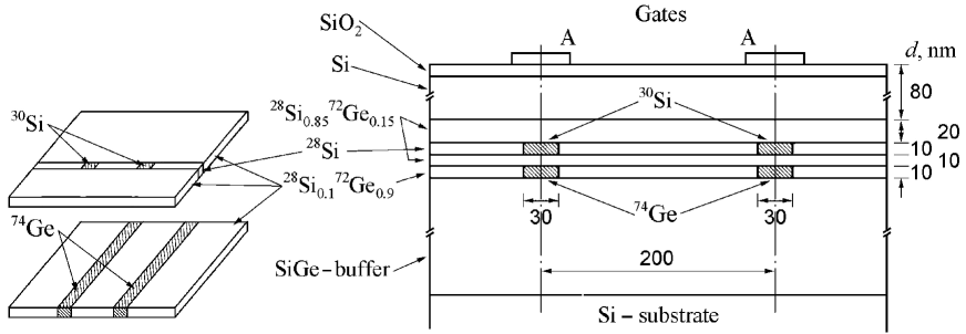
We suggest here a novel technology of the precise placing of P atoms into Si layer. The key point is the growth of the central Si and barrier Si0.85Ge0.15 layers from different isotopes: the Si0.85Ge0.15 layers from isotopes 28Si and 72Ge and the central Si layer from isotope 28Si with 30Si spots introduced by means of the nano-lithography (Fig. 1). The formation of quasi-one-dimensional Si wires will be achieved in a subsequent operation by the etching of Si layer between wires and the filling of the resulting gaps by the Si0.85Ge0.15 barrier composed from isotopes 28Si and 72Ge. Because different isotopes of Si and Ge are chemically identical, this technology guarantees the high quality of the grown structures.
After preparation, these structures will be irradiated with a neutron flux in a nuclear reactor followed by the fast annealing of radiation damage. The behaviour of different isotopes is different. After capture of a slow (thermal) neutron, a given isotope shifts to the isotope with mass number larger by one. If the isotope thus obtained is stable, this nuclear reaction does not entail doping. However, if the obtained isotope is unstable, it transmutes after half-life time to a nucleus of another element with atomic number larger by one in the case of decay. This method of doping is called NTD - neutron-transmutation doping NTD . In the case of Si, NTD is based on the transmutation of the isotope 30Si:
In the isotopically engineered structure, 31P donor atoms will be produced only within 30Si spots, because the isotopes 28Si and 72Ge shift to the stable isotopes 29Si and 73Ge, respectively. Therefore, in the suggested method, the processes of the structure growth and doping are completely separated. The idea to fabricate a basic element for a nuclear spin quantum computer using the isotope engineering of Si and SiGe nanostructures was proposed earlier in Shlimak1 ; Ladd . The precise placing of P atoms into a Si matrix by means of the NTD method was suggested in Shlimak2 .
Let us estimate the feasibility of the proposed method. We consider a 30Si spot of area nm cm2, thickness 10 nm with a distance of 200 nm between spots (Fig. 1). The ”buried” distance to the structure surface is halved, 100 nm, which is needed to protect against cross-links and to ensure the influence of the A-gate voltage on the corresponding underlying qubit only. In the proposed method of incorporation of P into Si, the vertical accuracy of the location of P donors is determined by the thickness of the 30Si spot (10 nm) with respect to the distance to the A-gate (100 nm). Indeed, the irradiation of samples by thermal neutrons occurs at room temperatures where the introduced P atoms are immobile. The irradiation is followed by the annealing of radiation damage at higher temperatures (700∘C). During the short annealing time (1 hour), impurities cannot diffuse far from the transmutation place; the diffusion length does not exceed 1–2 nm. As a result, the proposed method will provide an almost equal burying depth of P atoms with a controlled accuracy (about 10 % in our example). The time needed for the irradiation of the grown structures in a nuclear reactor is estimated as follows. The number of transmutation events is , where is the number of atoms, is the cross-section of the thermal neutron capture for given isotope ( cm2), is the integral neutron flux ( is the intensity of the thermal neutron flux and is the time of irradiation). In a spot with volume nm cm3, there are Si atoms ( cm-3). If the enrichment of Si with isotope 30Si is close to 100 %, . To achieve , the integral irradiation dose has to equal to neutron/cm2. In some research nuclear reactors, cm-2 s-1, which corresponds to the reasonable irradiation time s hrs.
II.2 Qubit certification
An unavoidable peculiarity of the NTD is the casual character of the neutron capture. As a consequence, after NTD, some of 30Si spots will contain no donor atom (“0-spot”) and cannot serve therefore as qubits, while some will contain more than one donor atom. The probability to find “0-spot”, “1-spot”, “2-spot”, and so on , is described by the Poisson distribution:
where is the binomial coefficient, is the probability for the neutron to be captured in a layer of thickness , is the dimensionless dose of irradiation.
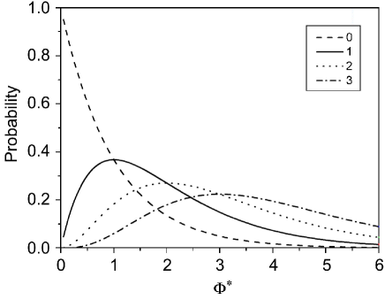
These probabilities are plotted in Fig. 2 as a function of the dimensionless parameter The best candidates for qubits are “1-spots”, while spots having more than one donor could also be considered as qubits after corresponding theoretical investigation. Only spots without donors (“0-spots”) are obviously non-qubits. In the NTD method, the maximal portion of “1-spots” is 37 % at . In this case, the portion of non-qubit is also about 37 %. If “2-spots” are also considered as possible qubits, the optimal integral dose will correspond to In this case, the fraction of non-qubits decreases to 14 %.
To determine the number of donors in each spot, we propose to use narrow source-drain (SD) channels fabricated beneath each donor position (Fig. 1). If the given spot contains one donor, it will form (together with the underlying SD channel and overlying A-gate) a flash-memory field-effect transistor (FET) with the qubit donor acting as a ”floating gate”. The donor electron is separated from the SD channel and A-gate by the Si0.85Ge0.15 barriers of about 10–20 nm width and 100 meV height Kane1 which are used for the electron confinement. However, a pulse of relatively strong voltage applied between the A-gate and SD channel will tilt the barriers leading to electron transfer and donor ionization. It was shown in Ref. Smit, that if the dopant-gate separation distance is more than 8 nm for P in Si (in our case this condition is satisfied because the distance to the gate is about 100 nm), the transfer of electron from donor takes place abruptly at a threshold voltage. An electric field of the positively-charged donor ion located only 10 nm from the narrow SD channel will shift the FET cutoff voltage at the value of about 10 mV, which is easy to observe Streetman . If there are two or more donors in the given spot, the cutoff shift will be even larger. If there is no donor underneath the given gate, the shift will not be observed.
II.3 Read-out operation
We believe that the proposed SD channel can also be used for the read-out operation, i.e. for the detection of a single nuclear spin state. The direct control of a nuclear spin state via nuclear magnetic resonance (NMR) measurements is a difficult problem. In Ref. Machida, , coherent control of the local nuclear spin was demostrated, based on pulsed NMR in a quantum Hall device. In Ref. Yusa, , a self-contained semiconductor device is described that can control nuclear spins in a nano-scale region. Measurements of the electron spin state are much easier taking into account the possibility of a spin-to-charge conversion for electrons. In accordance with the Kane model Kane98 , the state of the nuclear spin 31P is mediated by the spin of donor electron via the hyperfine interaction. Therefore, the task is to determine the spin orientation of the corresponding donor electron. The suggested method Vrijen is based on the fact that at low temperatures, a donor atom can capture the second electron with small ionization energy, about 1 meV, which results in the appearance of a negatively charged donor (-center). However, this process is possible only when the spin orientation of the second electron is opposite to that of the first electron. The appearance of the charged donor in the vicinity of the narrow SD channel will affect the current Kurten ; Xiao and can therefore be detected. As a result, one can determine the spin orientation of two neighboring donor electrons if one applies a potential difference between the corresponding A-gates which will cause the electron to jump from one donor to another . If we choose the spin orientation of the given donor as a reference, one can determine the spin state of the neighboring qubits on the right and left sides.
II.4 Source-drain channels fabrication
The proposed SD channels have a twofold purpose: the determination of the number of donors within each spot (qubit certification) and the determination of the spin state of the donor electron (read-out operation). We suggest a method for the fabrication and the proper alignment of the SD channels with respect to the position of 31P qubits. This method is also based on isotope engineering of a Si1-xGex layer followed by NTD. We propose to make the underlying Si1-xGex layer from a composition close to pure Ge (say, Si0.1Ge0.9) using isotopes 28Si and 72Ge, followed by the fabrication of 30 nm-width strips where 72Ge is replaced by 74Ge (Fig. 1). After NTD, these 74Ge-strips will be doped by As donors through the following nuclear reaction:
Irradiation of the structure with the thermal neutron integral dose cm-2 () needed for introducing on average one P donor in each 30Si spot, will also lead to doping of 74Ge-strips with As donors to a high level ( cm because of the relatively large cm2. This concentration of As exceeds the critical value of the metal–insulator transition for Ge:As Shlimak . Therefore, NTD-introduced narrow channels will have a metallic-like conductivity and remain conductive down to . This is important because nano-FET will operate at low temperatures when donor electrons in 31P-qubits are localized on their donors. For the suggested geometry of the SD channel, with the thickness of the Si0.1Ge0.9 layer of about 10 nm, width of the 74Ge-strips of 30 nm and the length about 1 m, the channel resistance is about 1 M, which is suitable.
In the proposed method of device fabrication, the proper alignment of the 74Ge-strips with respect to the overlying 31P qubits is provided by the high accuracy of the electron beam-assisted patterning of trenches in 72Ge28Si layer with the overlying holes in 28Si layer. Taking into account that the size of all components is not less than 30–50 nm, one can conclude that the alignment could be realized by the recent progress in SEM- and AFM-assisted lithography.
III Two-qubit operation
In this section, we suggest a new mechanism of entanglement for distant qubits and discuss, first, the principles of two-qubit operation. It has been shown DiVincenzo-2 that two-bit gates applied to a pair of electron or nuclear spins are universal for the verification of all principles of quantum computation.
Because direct overlap of wavefunctions for electrons localized on P donors is negligible for distant pairs, we propose another principle of coupling based on the placement of qubits at fixed positions in a quasi-one-dimensional Si nanowire and using the indirect interaction of 31P nuclear spins with spins of electrons localized in the nanowire which we will call hereafter as ”1D-electrons”. This interaction depends on the amplitude of the wavefunction of the ”1D-electron” estimated at the position of the given donor nucleus and can be controlled by the change in the number of ”1D-electrons” in the wire.
At the interqubit coupling is totally suppressed, each 31P nuclear spin interact only with its own donor electron. This situation is analoguous to that one suggested in the Kane proposal Kane1 and therefore all single-qubit operations and estimates of the decoherence time are valid also in our case. The difference consists in the method of coupling when a controlled number of ”1D-electrons”is injected into the nanowire. In this case, nuclear spin-qubits will also interact with the spins of ”1D-electrons”. To estimate the intensity of this interaction we need to calculate In the below calculation we believe that the donor potential does not influence the distribution function of ”1D-electrons” because it is screened by the donor electron on the relatively short distance of order of nm and is small comared with the wire length .
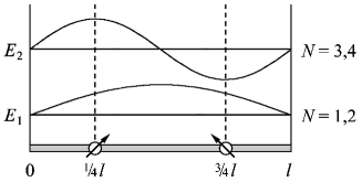
Let the interqubit distance be nm, one order of magnitude larger than in the Kane proposal Kane98 . To realize the coupling between these distant qubits, we suggest fabricating a Si nanowire of length nm and place P donors at distances , and (see Fig. 3). For and the functions belong to the energy levels () because each level contains two electrons with opposite spin. The highest amplitude of evaluated at the positions of the nuclear spin qubits and is realized at . In this case, the interqubit coupling is maximal.
To calculate the coefficient of the hyperfine interaction between nuclear and electron spins, we consider following PVW03 , a system consisting of electrons confined by a potential and two nuclear spins. We suppose that the nuclear spins are located far enough from each other so that the direct nuclear spin interaction is negligible. The contact hyperfine interaction between electrons and nuclear spins leads to an indirect nuclear spin interaction. Let the quantum wire have finite length in the -direction with the two nuclear spins located at and in a magnetic field directed in the direction. The Hamiltonian of the system is given by
| (1) |
where is the Hamiltonian of the electron in the mesoscopic structure in the magnetic field, is the contact hyperfine interaction, is the electron mass, is the magnetic-field potential, is the Bohr magneton, is the nuclear gyromagnetic ratio, and are nuclear and electron spins, and is radius vector of the nucleus.
The effective nuclear spin interaction energy calculated by second-order perturbation theory is Abragam :
| (2) |
Here, and are the eigenfunctions and eigenvalues of and is the electron distribution function in the initial and final states. We will use expression (2) to find the effective interaction between nuclear spins.
We suppose that the transverse dimensions of the quantum wire are much smaller than its length and the cyclotron orbit of the electron. The confining potential is , where if , and otherwise.
The wave function should satisfy the following boundary condition: . The solution has the form
| (3) |
| (4) |
where and are the transverse dimensions of the electron wave function.
Let us consider the problem at . In this case the electron distribution function is 1 for the filled states and 0 for the empty states. Inserting this wave function into Eq. (2) and assuming that the Zeeman splitting energy in (4) is much less than the energy gap between levels with different , one obtains the following expression for the nuclear spin interaction constant PVW03 :
| (5) |
It is seen, that at , is maximal for both qubit positions and . Let us estimate the error caused by unavoidable fluctuations in the positions of nuclear spins in the wire. In our device, the size of 30Si-spot is 30 nm. Therefore, one can expect that the position of NTD-introduced P donor will fluctuate around the central point within nm, which is about 1/40 of the total wire length (600 nm), . In our model, the coupling is realized in the case when the wave function of ”1D-electron” has the maximal value at places of the qubit location, where the space derivative is close to zero. This makes the coupling insensitive to the form of distribution function and to small fluctuations in the qubit positions.
Thus, the above consideration shows that the indirect coupling is maximal at while at the coupling is totally suppressed. This means that in our model, the entanglement between two distant qubit can be effectively controlled by the proper variation of .
IV Scalability
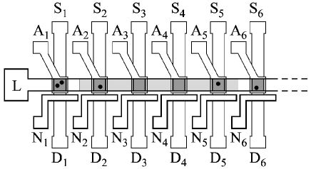
Scalability is the one of the most important requirements of the quantum computer proposals DiVincenzo . We suggest below the schematics of the device architecture (Fig. 4) which satisfy the scalability requirements. It is worth mentioning that the above method of coupling opens a way to avoid the problem connected with the break in the one-dimensional array of qubits. This problem is inevitable in all proposed technologies. In the method of coupling based on the direct overlap of electron wave functions Kane98 ; Vrijen , this requirement is crucial because any break in the one-dimensional array of qubits stops the entanglement along the array and make quantum computation impossible. In our model, entanglement can exist even in the unlikely case of two or more breaks in the qubit array one after another, because indirect coupling can passing over wrong sites by the proper choice of the nanowire length and the number of electrons in the wire.
Figure 4 shows the schematics of the device architecture which allows one to vary and . The device consists of a 28Si nanowire with an array of 30Si spots. Each spot is supplied by the overlying A-gate, the underlying SD-shannel and the lateral N-gate. After NTD, P donors will appear in most of the spots (which transforms these spots into qubits) and not appear in other spots (non-qubits). This situation is shown schematically in Fig. 4 where one assume that the spots 3 and 4 are non-qubits (”0-spots”) and one need to provide coupling between qubits and . For this purpose, it is necessary to connect the gates N2, N3, N4 and N5. The negative voltage applied between other N-gates and the wire contact will lead to pressing-out ”1D-electrons” from all corresponding areas and formation of the nanowire with nm between the sites 2 and 5 only (shown in grey in Fig. 4). The coupling between qubits and will be realized via injection in the wire of the necessary number of electrons , using the positive voltage applied to the gates N2–N5. In this particular example, the maximal coupling will be realized at , while at , the coupling will be totaly suppresed.
V
Summary
A new method of a quantum information processing is suggested based on the precise placing of 31P nuclear spin qubits in a quasi-one-dimensional 28Si nanowire. The fabrication method includes the isotope engineering of Si and SiGe layers followed by the neutron-transmutation doping of the obtained structures. The interqubit coupling is based on the indirect interaction of 31P nuclear spin with the spin of electron localized in the nanowire. The advantage of the proposed method of operation consists in its ability to control the coupling between distant qubits and even between qubits separated by non-qubits nodes in a one-dimensional array. The last feature allows one to develop the basic unit and the scalable architecture of a nuclear spin-based quantum computer. Numerical estimates show the feasibility of the proposed methods.
VI Acknowledgements
We are thankful to P. Wyder and Yu.V. Pershin for fruitful discussions. I.S thanks the Erick and Sheila Samson Chair of Semiconductor Technology for financial support. I.V. acknowledges the support of the Brussels program EuroMagNET RII3-CT-2004-506.
References
- (1) D. P. DiVincenzo, Fortschr. Phys. 48 (9–11), 771 (2000).
- (2) D. Loss and D. P. DiVincenzo, Phys. Rev. A 57, 120 (1998).
- (3) V. Privman, I. D. Vagner, and G. Kventsel, Phys. Lett. A 239, 141 (1998).
- (4) B. E. Kane, Nature 393, 133 (1998).
- (5) B. E. Kane, Fortschr. Phys. 48 (9–11), 1023 (2000).
- (6) R. Vrijen, E. Yablonovitch, K. Wang, H. W. Jiang, A. Balandin, V. Roychowdhury, T. Mor, and D. DiVincenzo, Phys. Rev. A 62, 012306 (2000).
- (7) R. G. Clark et al., Phil. Trans. R. Soc. Lond. A 361, 1451 (2003).
- (8) J. L. O’Brien, S. R. Schofield, M. Y. Simmons, R. G. Clark, A. S. Dzurak, N. J. Curson, B. E. Kane, N. S. McAlpine, M. E. Hawley, and G. W. Brown, Phys. Rev. B 64, 161401(R) (2001).
- (9) S. R. Schofield, N. J. Curson, M. Y. Simmons, F. J. Ruess, T. Hallam, L. Oberbeck, and R. G. Clark, Phys. Rev. Lett. 91, 136104 (2003).
- (10) C. Yang, D. N. Jamieson, C. Pakes, S. Praver, A. Dzurak, F. Stanley, P. Spizziri, L. Macks, E. Gauja, R. Clark, Jpn. J. Appl. Phys. 42, 4124 (2003).
- (11) S.-J. Park, A. Persaud, J. A. Liddle, J. Nilsson, J. Bokor, D. H. Schneider, I. W. Rangelow, T. Schenkel, Microelectronic Engineering 73-74, 695 (2004).
- (12) A. Persaud, S. J. Park, J. A. Liddle, I. W. Rangelow, J. Bokor, R. Keller, F. I. Allen, D. H. Schneider, T. Schenkel, Quantum Information Processing 3, 233 (2004).
- (13) A. A. Larionov, L. E. Fedichkin, A. A. Kokin, and K. A. Valiev, Nanotechnology 11, 392 (2000).
- (14) R. W. Keyes, Appl. Phys. A 76, 737 (2003).
- (15) Neutron Transmutation Doping in Semiconductors, edited by Meese J. (Plenum Press, New York, 1979).
- (16) I. Shlimak, V. I. Safarov and I. D. Vagner, J. Phys.: Condens. Matter 13, 6059 (2001).
- (17) T. D. Ladd, J. R. Goldman, F. Yamaguchi, Y. Yamamoto, E. Abe and K. M. Itoh, Phys. Rev. Lett. 89, 017901 (2002).
- (18) I. Shlimak and I. D. Vagner, In: Recent Trends in Theory of Physical Phenomena in High Magnetic Fields, edited by I. D. Vagner et al. (Kluwer Academic Publishers, Printed in the Netherlands, 2003), p.281.
- (19) G. D. Smit, S. Rogge, J. Caro, and T. M. Klapwijk, Phys. Rev. B 68, 193302 (2003).
- (20) B. G. Streetman and S. Banerjee, Solid State Electronic Devices, 5th ed. (Prentice Hall, 2000).
- (21) T. Machida, T. Yamazaki, K. Ikushima, S. Komiyama, Appl. Phys. Lett. 82, 409 (2003).
- (22) G. Yusa, K. Muraki, K. Takashina, K. Hashimoto, Y. Hiroyama, Nature, 434, 1001 (2005).
- (23) M. J. Kurten and M. J. Uren, Adv. Phys. 38, 367 (1989).
- (24) M. Xiao, I. Martin, H. W. Jiang, Phys. Rev. Lett. 91, 078301 (2003).
- (25) I. Shlimak, M. Kaveh, R. Ussushkin, V. Ginodman, and L. Resnick, Phys. Rev. Lett. 77, 1103 (1996).
- (26) D. P. DiVincenzo, Phys. Rev. A 51, 1015 (1995).
- (27) Yu. V. Pershin, I. D. Vagner, and P. Wyder, J. Phys.: Condens. Matter 15, 997 (2003).
- (28) C. P. Slichter, Principles of Magnetic Resonance, 3rd ed. (Springer-Verlag, Berlin, 1992).