A novel mechanism of charge density wave in a transition metal dichalcogenide
Abstract
Charge density wave, or CDW, is usually associated with Fermi surfaces nesting. We here report a new CDW mechanism discovered in a 2-structured transition metal dichalcogenide, where the two essential ingredients of CDW are realized in very anomalous ways due to the strong-coupling nature of the electronic structure. Namely, the CDW gap is only partially open, and charge density wavevector match is fulfilled through participation of states of the large Fermi patch, while the straight FS sections have secondary or negligible contributions.
pacs:
71.18.+y, 71.45.Lr, 79.60.-iIt has been a standard textbook-example that charge density wave (CDW), one of the main forms of ordering in solid, is mostly associated with nesting Fermi surface (FS) sections. In charge ordered materials ranging from one-dimensional (1D) (TaSe4)2I and blue bronzeDardelPRL ; DardelEPL to two-dimensional (2D) manganites, and from surface reconstruction in weak correlated metals to checker board pattern of strongly correlated high temperature superconductorsShenKM ; Nakagawa , the charge fluctuations associated with the ordering wave vector scatter the electrons between two nested FS sections and effectively drive the system into an ordered ground state. However, this classical picture failed in the very first 2D CDW compound discovered in 1974, i.e. the transition metal dichalcogenides (TMD's)WilsonAP . The 2-structured TMD's have a hexagonal lattice structure, and in its CDW phase, a superlattice formsWilsonAP ; Moncton1 . It was found that the ordering wavevectors do not match the nested FS sections, and generally no CDW energy gap was observed at the FSRossnagelPRB ; TonjesPRB . After decades of continuous effort, the origin of CDW for the -structured TMD's has been a long standing mystery. As a result, the subtle details of the competition and coexistence of CDW and superconductivity in TMD'sCastro remain to be revealedshinScience .
In this letter, we studied the electronic origin of the CDW in a 2-TMD, -NaxTaS2, by angle-resolved photoemission spectroscopy (ARPES). The CDW mechanism in this material was discovered after the revelation of the following exotic properties. i) The electronic structure exhibits strong coupling nature, with finite density of states at the Fermi energy() over almost the entire Brillouin zone(BZ), forming so-called Fermi patches. ii) In the CDW state, only a fraction of the states at is gapped. iii) The density of states near directly correlates with the ordering strength. iv) Fermi patch, instead of Fermi surface, is relevant for CDW. We show that this new ``Fermi-patch mechanism" for CDW is rooted in the strong coupling nature of the electronic structure and it may be a general theme of ordering in the strong coupling regime of various models, and applicable to systems with similar electronic structure.
For the systematic studies of the electronic structure in a 2-TMD compound, 2-NaxTaS2 with 2, 5 and 10 Na concentration were synthesized with CDW transition temperature TCDW's are 68K, 65K and 0K respectively. The samples are labelled as CDW68K, CDW65K, and CDW0K hereafter. The corresponding superconducting transition temperatures are 1.0K, 2.3K and 4.0K respectively, a manifestation of the competition between CDW and superconductivity in this system. The data were mainly collected using 21.2eV Helium-I line of a discharge lamp combined with a Scienta R4000 analyzer, and partial measurements were carried out on beam line 5-4 of SSRL. The overall energy resolution is 8 , and the angular resolution is 0.3 degrees.
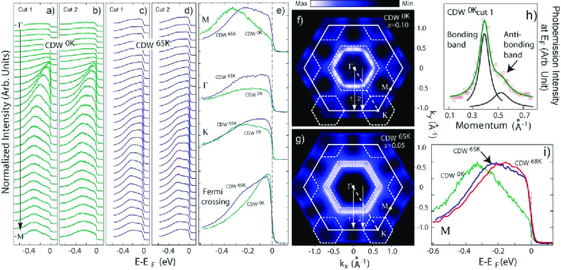
Photoemission spectra taken on samples with (CDW65K) and without CDW (CDW0K) are compared in Fig. 1a-d. In both cases, the spectral lineshapes are remarkably broad, and no quasiparticle peaks in the conventional sense are observed. The large linewidth is of the same order as the dispersion, which clearly indicates the incoherent nature of the spectrum and the system is in the strong coupling regime. Taking the normalized spectra at M as referenceexp1 , spectra at , K, and the Fermi crossing of the -M cut are compared in Fig. 1e. The difference between CDW0K and CDW65K is striking. Although they have similar density of states at the Fermi crossing area, for momentum regions away from the FS, CDW65K has much stronger spectral weight than CDW0K, no matter whether it is inside the occupied region (M point), or in the unoccupied region ( and K points) in the band structure calculationsGuo . Particularly, one finds that even when the spectral centroid is well below , the finite residual weight at beyond background exists around M. We note that the CDW0K sample has higher Na doping than CDW65K, yet its lineshape is generally sharper. Therefore, disorder effects induced by the dopants should be negligible. The residual weight observed near thus should be associated with the intrinsic strong coupling nature of the system, which (within several around ) shows a monotonic correlation with TCDW in Fig. 1i.
Although the spectra are broad, Fermi surfaces could still be defined as the local maximum of the spectral weight at KipPRL , which are plotted in Fig. 1f-g for CDW0K and CDW65K respectively. Three FS pockets can be identified through the momentum distribution curve analysis: two hole pockets around , as exemplified in Fig. 1h, and one hole pocket around K. Bilayer band splitting of the two TaS2 layers in a unit cell manifests itself as the inner and outer Gamma pockets, while the splitting of the K pockets is indistinguishable. The FS volumes are evaluated to be and electrons per layer for the 5 and 10 Na doped NaxTaS2 samples respectively, consistent with the nominal dopant concentrations. This resembles the high temperature superconductors, where the Fermi surfaces defined in this conventional way are consistent with the band structure calculations and follow the Luttinger sum rule quite welldinghongPRL1997 , yet there are large Fermi patches near the antinodal regionsFurukawaPRL . In CDW65K case, almost the entire BZ appear to be one gigantic Fermi patch. However, so far, searches for the CDW mechanism are mostly centered on the Fermi surfaces, not the Fermi patch.
The differences between CDW65K and CDW0K spectra in the Fermi patch region(Fig. 1e) are intriguing. Fig. 2a-b show spectra taken from M at different temperatures for CDW65K and CDW0K respectively. While the CDW0K spectra simply exhibit a clear Fermi crossing and thermal broadening, the CDW65K spectra appear very anomalous. Take the spectrum at 7K as an example, while the upper part of the spectrum is suppressed to higher binding energies, the middle point of the leading edge of the lower part still matches . There is an apparent turning point between these two parts of the spectrum. By dividing the spectra with the corresponding finite temperature Fermi-Dirac distribution functions, in Fig. 2c, one clearly observes that about 29% of the spectral weight at has been suppressed for CDW65K. An energy gap has opened on part of the states here, which is estimated to be 35 based on the middle point of the leading edge. Contrastively, there is no sign of gap opening for CDW0K (Fig. 2d).
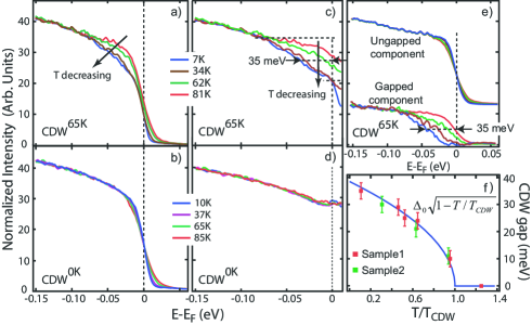
It was recently suggested by Barnett and coworkersBarnettPRL that a 2-TMD system is decoupled into three sub-lattices. While one of the sub-lattices is undistorted and gapless below TCDW, the other two are gapped at the FS. For CDW65K, similar behavior is observed except that gap does not open at Fermi Surface and just about 1/3 of the spectrum is gapped. Phenomenologically, one can decompose the spectra into gapped and ungapped components. The ungapped component is simulated as
, where is the spectral function, is the resolution convoluted finite temperature Fermi-Dirac distribution function, and . The gapped components
. The decomposition of spectra in Fig. 2a is shown in Fig. 2e, where the ungapped components exhibit the same behavior as in the CDW0K spectrum, and the gapped components clearly reveal a clean energy gap of about 35meV at 7K. We emphasize that although the decomposition method is adopted hereafter, all the qualitative results can be obtained through the conventional method in Fig. 2c as well. The temperature evolution of the gap is shown in Fig. 2f for two different CDW65K samples. Interestingly, the gap does not saturate at low temperature, and it can be fitted very well to , which is the mean field theory form at temperature close to TCDWGruner . Here the fitted 396TCDW.
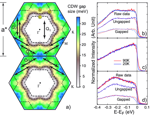
Spectra at other momenta could be decomposed in the same way quite robustlyexp3 , and the CDW gap was mapped over the entire Brillouin zone for CDW65K (Fig. 3a). Strikingly, finite CDW gap exists over most of the Brillouin zone. Its maximum locates around M, and no gap is observed around the inner Fermi pocket and within. Noticeably, the gap is finite in the K Fermi pockets, as there is finite spectral weight at . Close comparisons of spectra at various momenta are shown in Fig. 3b-d. In between M and the Fermi crossing (Fig. 3b), the upper part of the low temperature spectrum is overlayed with the normal state spectrum, which is a sign of gap opening. In Fig. 3c, for spectrum at the inner Fermi pocket, no sign of gap opening is observed, consistent with previous studiesRossnagelPRB ; TonjesPRB . Fig. 3d illustrates that a gap of 15 is observed at the saddle point of the band calculation. An alternative mechanism was proposed for 2-TMD's involving the scattering between saddle points, which would cause a singularity in density of states, and thus an anomaly in the dielectric response functionRicePRL . The gap near this point has been reported beforeLiuPRL , but the distance between these points do not match the CDW ordering wavevectorsStraub ; Rossnagel . In the current gap map, nothing abnormal is observed for this momentum.
The CDW in TMD's is associated with structural transitionsWilsonAP ; Moncton1 , therefore, electron-phonon interactions are also crucial in the problem. Since the low energy electronic structure of 2-NaxTaS2 is dominated by the Ta 5d electrons Guo , among which Coulomb interactions are usually weak, the broad ARPES lineshape would suggests strong electron-phonon interactions. A kink in the dispersion corresponding to the phonon energy scale was found for 2-NaxTaS2 (not shown here) as in other 2H-TMD compoundsValla . In this context, the anisotropic gap distribution might be attributed to the anisotropy of electron-phonon couplings TD ; Valla2004 , and states in the ungapped region simply may not couple with the relevant phonons. One critical requirement, i.e. states in different gapped regions need to be coupled by phonons with the CDW wavevectors, can now be fulfilled in the gap map, as illustrated by the arrows in Fig. 3a. Qi=ai*/3,(i=1,2,3) here are the CDW wavevectors, ai*'s being the reciprocal lattice vectors along the three -M directions. This also explains why the size of the Fermi surfaces can vary significantly for different 2H-TMD systems, with nearly system-independent CDW ordering wavevectorsStraub ; Rossnagel ; Moncton2 .
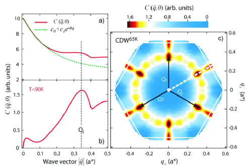
One open question in the above picture is that charge fluctuations with other wavevectors are also allowed, and it is not obvious why Qi's are special. For cuprate superconductors, it has been demonstrated that the autocorrelation of ARPES spectra,
, could give a reasonable count for the charge modulations observed by STMChatterjee ; McElroy . This joint density-of-states describes the phase space for scattering of electrons from the state at to the state at by certain modes with wavevector . Therefore, one would expect that it peaks at the ordering wavevector for near the phase transition of static order. Since the states in the gapped Fermi patch are responsible for the CDW here, autocorrelation analysis is conducted in the normal state to study the CDW instabilities of over regions that would be gapped below . The resulting is shown in Fig. 4a for along the -M direction, which is mainly consisted of a component at that exponentially decays, and several features in Fig. 4b, where a peak is clearly observed around the CDW ordering wavevector. The peak at would require coupling to very long wavelength phonons, which presumably is very weak. Consistently, a recent calculation has shown that an optical phonon branch softens significantly around Qi, and no sign of softening is observed at Lin . In the 2D partial map (obtained after deducting the exponential decaying part and the constant background)in Fig. 4c, although there are a few local maxima corresponding to various possible orderings, the highest peaks are those at Qi. Therefore, our results suggest that the electronic structure is in favor of the charge instability at Qi's, and eventually the system becomes unstable to the CDW formation below in collaboration with the phonons. Furthermore, it is also consistent with the positive correlation between the spectral weight near and TCDW in Fig. 1i.
The competition and coexistence of CDW and superconductivity can be understood within the new framework. Recent photoemission studies have revealed that superconducting gap opens at the K and pocketsshinScience ; Valla2004 . The CDW gap opens at a temperature higher than the superconducting transition, but it just partially suppresses the density of states around the K pocket and outer pocket. Therefore, as observed in most -TMD's, superconductivity is suppressed but not eliminated by the CDW.
To summarize, the Fermi-patch mechanism of CDW in 2-NaxTaS2 is characterized by the realization of both ingredients of the CDW, energy gap and wavevector match on the Fermi patches. Unlike other CDW mechanisms based on band structure effects, it is rooted in the strong-coupling nature of its electronic structure, which provides phase space needed for CDW fluctuations. Furthermore, this mechanism would be realized not only in polaronic systems, but also in materials where strong electron correlations could cause Fermi patches, and thus CDW instabilities.
We thank Profs. H. Q, Lin, J. L. Wang, Q. H. Wang, J. X. Li, Z. D. Wang and F. C. Zhang for helpful discussions. This work is supported by NSFC, MOST's 973 project: 2006CB601002 and 2006CB921300.
References
- (1) B. Dardel et al., Phys. Rev. Lett. 67, 3144 (1991).
- (2) B. Dardel et al., Europhys. Lett. 19, 525 (1992).
- (3) K. M. Shen et al., Science 307, 901 (2005).
- (4) T. Nakagawa et al., Phys. Rev. Lett. 86, 854 (2001).
- (5) J. A. Wilson, F. J. Di Salvo and S. Mahajan, Adv. Phys. 24, 117 (1975).
- (6) D. E. Moncton, J. D. Axe and F. J. Di Salvo, Phys. Rev. Lett. 34, 734 (1974).
- (7) K. Rossnagel et al., Phys. Rev. B 72, 121103 (2005).
- (8) W. C. Tonjes et al., Phys. Rev. B 63, 235101 (2001).
- (9) A. H. Castro Neto, Phys. Rev. Lett. 86, 4382 (2001).
- (10) T. Yokoya et al., Science 294, 2518 (2001).
- (11) L. Fang et al., Phys. Rev. B 72, 014534 (2005).
- (12) This normalization also matches the valence band at higher binding energies reasonably.
- (13) G. Y. Guo and W. Y. Liang, J. Phys. C: Solid State Phys. 20, 4315 (1987).
- (14) L. Kipp et al., Phys. Rev. Lett. 83, 5551 (1999).
- (15) H. Ding et al., Phys. Rev. Lett. 78, 2628 (1997).
- (16) N. Furukawa, T. M. Rice and M. Salmhofer, Phys. Rev. Lett. 81, 3195 (1998).
- (17) R. L. Barnett et al., Phys. Rev. Lett. 96, 026406 (2006).
- (18) G. Grüner, Density Waves in Solids. (Addison-Wesley Longman, 1994)
- (19) The same is used for the entire zone, and we have checked that the gap size varies within against a change of .
- (20) T. M. Rice and G. K. Scott Phys. Rev. Lett. 35, 120 (1975).
- (21) R. Liu et al., Phys. Rev. Lett. 80, 5762 (1998).
- (22) Th. Straub et al., Phys. Rev. Lett. 82, 4504 (1999).
- (23) K. Rossnagel et al., Phys. Rev. B 64, 235119 (2001).
- (24) T. Valla et al., Phys. Rev. Lett. 85, 4759 (2000).
- (25) T. Valla et al., Phys. Rev. Lett. 92, 086401 (2004).
- (26) T. P. Devereaux, T. Cuk, Z.-X. Shen and N. Nagaosa, Phys. Rev. Lett. 93, 117004 (2004).
- (27) D. E. Moncton, J. D. Axe and F. J. Di Salvo, Phys. Rev. B 16, 801 (1977).
- (28) U. Chatterjee et al., Phys. Rev. Lett. 96, 107006 (2006).
- (29) K. McElroy et al., Phys. Rev. Lett. 96, 067005 (2006).
- (30) J. L. Wang and H. Q. Lin, preprint.