Microscopic origin of critical current fluctuations in large, small and ultra-small area Josephson junctions.
Abstract
We analyze data on the critical current and normal state resistance noise in
Josephson junctions and argue that the noise in the critical current is due
to a mechanism that is absent in the normal state. We estimate the noise
produced by conventional Two Level Systems (TLSs) in the insulating barrier and
find that it agrees both in magnitude and in temperature dependence with
the resistance fluctuations in the normal state but it is not sufficient to
explain the critical current noise observed in large superconducting contacts.
We propose a novel microscopic mechanism for the noise in the superconducting state
in which the noise is due to electron
tunneling between weak Kondo states at subgap energies. We argue that the noise
produced by this mechanism gives temperature, area dependence and
intensity that agree with the data.
pacs:
85.25.Cp, 03.65.Yz,73.23.-bIntroduction. The microscopic mechanism at the origin of critical current fluctuations in Josephson junctions is a long standing open problem. A phenomenological characterization of critical current noise began with the experiments in large Niobium junctions in the late ’s Wellstood (1988); in these experiments the critical current fluctuations were inferred from the fluctuations in the current of resistively shunted junctions biased by a low voltage that has no effect on the superconductivity of the contacts themselves. It was found that the noise power spectra display behavior for low frequencies temperature dependent intensity Wellstood et al. (2004) and that it also scales with the inverse area of the junction with coefficient that depends, albeit weakly, on the superconducting or insulating barrier material Harlingen et al. (2004).
It is natural to attribute the critical current fluctuations to charges that move between different localized states in the junction barrier Rogers and Buhrman (1985b). However, a more detailed comparison with the experiments reveals serious problems with this picture. In this model, each fluctuator is similar to a glassy TLS Burin (1995), so one expects that the distance between the levels and the tunneling barrier have a broad distribution on the atomic energy scale. Quantum tunneling or thermal activation leads to the charge motion between two states which changes the barrier height and thus leads to a noisy Random Telegraph Signal (RTS) in the current through the junction Rogers and Buhrman (1984). A superposition of RTSs with a broad distribution of tunneling barriers leads to the noise power spectra Dutta and Horn (1981). The problem with this model is that TLSs and similar objects have a constant density of states at low energies and this would give a linear dependence of the noise power spectrum in contrast with the data. Alternatively, assuming that behavior comes from the linear density of states and extrapolating this density of states to atomic scales one gets unphysically large values for the density of these switches thus indicating the presence of some low energy scale in the problem.
Recently, the interest in critical current fluctuations was renewed because of their importance to the superconducting qubit dephasing and a new puzzle was added to the picture. The new experiments Eroms et al. (2006) studied the fluctuations in the small area Aluminium junctions, similar to the ones that are currently used for qubit implementations in the flux qubit Chiorescu et al. (2003), the phase qubit Martinis et al. (2002) and the quantronium Vion et al. (2002). The critical current noise was inferred from fluctuations in the normal state resistance of the junction. It has been observed that the noise power spectrum displays a behavior at low frequency but its temperature dependence is only linear and the intensity of the noise is two order of magnitude lower than the value reported for larger superconducting contacts.
In this Letter we argue that the problems with the microscopic model noted above as well as the inconsitency between the old and the new data are all removed if the main source of the critical current noise is electron trapping in shallow subgap states that might be formed at the superconductor-insulator boundary Faoro and Ioffe (2006). The electron tunneling between such traps contains two Fermi factors leading to the behavior with the energy scale , thereby eliminating the difficulties with the conventional model noted above. This model is further supported by the recent experiments performed in Single Electron Transistors that show dependence of the low charge noise power spectra in very small superconducting contacts Astafiev et al. (2004). We shall argue that this mechanism dominates the critical current noise in the superconductive regime but disappears in the normal state where these states become Kondo resonances leaving only a weaker conventional TLSs mechanism active that, at high temperatures, produces linear dependence of the noise power in agreement with the data Eroms et al. (2006). An important feature of the new mechanism is that the large number of subgap states is partially compensated by their small weight (a vestige of their Kondo resonance origin) Faoro and Ioffe (2006). Physically, it means that these states generate a featureless noise even in the smallest contacts. In contrast, in normal leads, where the noise is due to TLSs in the insulating barrier, our estimates show that the number of active fluctuators, especially in ultrasmall contacts, is low, in agreement with the data Rogers and Buhrman (1985a).
Below we discuss the details of the data and estimates of the noise produced in new and conventional microscopic models. We begin with the data.
Data. The directly measured low frequency noise () of the critical current turns out to be almost universal. The original experiments measured it in large contacts (area, , varying between ) made of Wellstood (1988); Wellstood et al. (2004). In these experiments the junctions were biased by a very low voltage that does not affect the superconductivity of the contacts (i.e. ) Cri . In these conditions, the noise power spectra are described by:
| (1) |
in a wide temperature range . Here is the critical current, and are the area and temperature scale which are conventionally set to and . Remarkably, the dimensionless proportionality coefficient, , is not sensitive to the details of the junction preparation and it is roughly (within a factor “universal ”: Harlingen et al. (2004). The noise observed in these experiments was usually featureless, evidently coming from many fluctuators, but in rare cases and at relatively high temperatures, one observes also a switching process between two well defined current values that disappears when temperature decreases below K. Notice that the quadratic growth of the noise with temperature that starts at implies that the number of fluctuators at atomic energies would be at least larger than their number at low temperatures and thus would exceed the number of atoms in contact (), providing the evidence of additional energy scale.
In a different set of experiments Eroms et al. (2006), the critical current of small junctions was not directly measured but extracted from their normal state resistance fluctuations. To perform measurements at very low temperatures, the junctions of area were subjected to the magnetic field above that suppressed the superconductivity in the contacts. It was found that for the noise power spectrum is well described by a linear -dependence:
| (2) |
with the intensity that is two order of magnitudes lower than that predicted by Eq. (1). Moreover, for temperatures below , it has been observed that the low frequency noise was due to few individual strong fluctuators. These observations are in a good agreement with the conventional TLSs picture of the noise origin. Indeed, in a typical structural glass one expects a constant density of states that leads to the linear temperature dependence of the noise and to the total number of the thermally excited TLSs, , in contact. These data are also in a qualitative agreement with the older measurements of ultrasmall ( junctions performed in the temperature range Rogers and Buhrman (1985a). In these measurements, the contacts either were kept normal due to a high temperature or they were very far from equilibrium due to a high voltage bias ; the observed low frequency noise was dominated by few fluctuators even at .
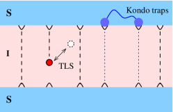
The detailed quantitative comparison between different data and microscopic estimates is made difficult by the possibility of the inhomogeneous current distribution through the insulating barrier. For instance, the newer data Eroms et al. (2006) report the relative variation of the resistivity due to one fluctuator corresponding to the change in the effective area of the junction by while for the older data Rogers and Buhrman (1985a) this value is . This difference explains why the noise in new experiments got dominated by a few fluctuators only below in contrast to Rogers and Buhrman (1984) where single fluctuators were resolved below . Indeed, it is difficult to imagine microscopic processes that affect large areas ; a more plausible explanation is that the conductance is dominated by relative small areas or channels in this system Buchanan et al. (2002) which decreases further the number of fluctuators (Figure 1). This conjecture is supported by the recent analysis Dorneles et al. (2003) that found that the conductive area is of the total. Most likely, however, this value depends strongly on the material preparation.
Microscopic mechanisms of decoherence. All mechanisms of the noise assume that it comes from the fluctuations in the state of the insulator that affect the tunneling barrier and thus the critical current. If these fluctuations are not affected by the state of the metal (superconductor or normal) they would equally affect the critical current and the normal state resistance according to the Ambegaokar-Baratoff formula: Ambegaokar and Baratoff (1963a). One can argue that these fluctuations might be due to fluctutating trapped electrons or randomly moving TLSs inside the barrier.
Low energy electrons trapped in the vicinity of the normal metal can tunnel into the metal; this process converts the sharp state into a short-living resonance. In superconductor, however, the low energy states disappear and the life time of these states increases. Notice that a large potential difference between the contacts provides electron states below the gap and thus makes the system effectively normal. In a superconductor a localized low energy electron can change its state only by tunneling into another subgap state via Andreev process Faoro et al. (2005). If the density of states for these subgap states is constant, the number of thermally active electrons and their possible final states both scale with temperature leading to behavior of the noise in agreement with the data. However, similarly to TLSs, the density of states for such traps is too little to account for the number of fluctuators observed experimentally.
We believe that the physical mechanism responsible for a dramatic increase in the density of states for the localized low energy electrons is the formation of Kondo-like resonances due to a large Coulomb repulsion between the electrons in the same trap Faoro and Ioffe (2006). In this picture, the characteristic energy scale for these resonances is given by the Kondo temperature which depends exponentially on the bare level width and the bare level position : . The natural assumption that is distributed in a broad range leads to distribution of Kondo temperatures in the normal state. In the superconductor the resonances having become localized low energy levels with a constant surface density of states where is the bare surface density of traps () and . The increase in the density of states of these objects is partially offset by the small weight of the Kondo resonance that translates into the small weight of the formed localized state.
The noise at frequency is due to the electron tunneling between two traps with rate . The exact calculation of the rate for two specific traps is a complicated problem but it is sufficient for our purposes to note that the latter is an exponential function of the bare parameters and thus it is characterized by distribution function. Indeed, in superconductors the tunneling amplitude falls exponentially with distance: where is the coherence length of the superconductor. Moreover, the tunneling between Kondo resonances is additionally suppressed by the small factor and finally, the electron tunneling between the states with different energies is also accompanied by the thermal phonon emission or absorption but the rate of these processes is much faster than the frequencies of interest () so the main dependence comes from the exponential factors mentioned above.
In order to estimate the critical current fluctuations induced by these tunneling processes we need to know the effect induced by a single electron trapped in a deep state. We shall describe it by the change in the effective area of the junction (i.e. ). For the quantitative estimates we shall assume that . The tunneling processes allow tunneling between the traps within energy from the Fermi surface located at distances from each other. Combining all factors we find that the noise spectrum generated by independent relaxational processes between the traps reads:
| (3) | |||||
where . This noise displays dependence and inverse proportionality to the area of the contacts in agreement with the data observed in large contacts. To estimate the intensity of the noise we assume that the distance between electron traps is roughly of the same order as the distance between TLSs in the bulk or (between typical surface defects) leading to Using the Nb parameters: , , , , we estimate the dimensionless parameter controlling the noise intensity at , obtaining which is in excellent agreement with the measured value (given the crude nature of the estimates).
Alternatively, critical current noise might be due to fluctuating TLSs in the insulating barrier Burin (1995). Most likely, TLSs correspond to atoms that can tunnel between two positions in the amorphous material. Two different states can be distinguished by the different values of the dipole moment. Thus, TLSs deep inside the insulator interact only weakly with electrons in the metal and are not affected by the superconductivity. Each quantum TLS is described by the Hamiltonian , where is the energy difference between the two minima and is the tunneling amplitude between them. Here is of the order of the frequency vibrations of the particle in the potential wells and is the tunneling action. In bulk amorphous materials and are distributed in a broad range leading to the distribution function . Generally, each TLS has states with energies that are occupied with thermal probability factors. At not-too-low temperatures () the TLS relaxation process is dominated by phonon emission or absorption that leads to the relaxation rate of the occupancy number where the coefficient depends on the details of the TLS-phonon interaction Kogan (1996). The dominant contribution to low frequency noise comes from thermally excited TLSs with low tunneling amplitudes . These TLSs are characterized by the distribution function . Each individual TLS contributes: to the current-current correlator. By assuming as before that each TLS affects the critical current by and by averaging over the TLSs distribution function we find that the total noise power spectrum originating from the uniform insulating barrier of thickness reads:
| (4) |
As expected this noise is proportional to and . Non uniform distribution of the current discussed above decreases the number of the effective TLSs because each TLS affects only the current that flows in a close vicinity of a moving atom. We describe this suppression by the dimensionless coefficient ; very crudely we can estimate where . For small Al contacts, , at we get , which is in agreement with the direct data on the normal state resistance fluctuations Eroms et al. (2006) . Notice that a relative small value of the effective area for these contacts implies that the current is relatively homogeneous; one expects smaller values for the contacts studied earlier Rogers and Buhrman (1985a) for which similar estimates gives a larger result which is however still smaller that the noise observed directly in the superconducting state.
As a final remark, let us notice that the electron trap model for the noise in the superconducting state leads to an interesting prediction. Namely, the process of tunneling between these traps should also contribute to the high frequency dissipation leading to ohmic behaviour of the spectrum: . The proportionality constant, , in this formula has a meaning of the effective conductance of the contact due to the trapped electrons, i.e. , and it could be in principle extracted from measurements similar to the ones performed by Astafiev et al. Astafiev et al. (2004) for the charge noise. Here, however, such experiments are made difficult by the noise coming from the shunt resistors and the residual resistance of the contact itself due to charge fluctuators.
Conclusions. We identify a new microscopic mechanism responsible for the noise in the superconducting contacts. This mechanism contributes to the low frequency noise only in the superconducting state and it is due to the appearance of subgap states localized near the superconductor-insulator boundary. The resulting noise has homogeneous spectrum, dependence and it is inversely proportional to the surface area of the junction in agreement with the experiments. The estimates of its intensity are in a good agreement with experimental values. This mechanism disappears when the superconductivity of the contacts is suppressed. In the normal state the noise is generated by the thermally excited TLSs. In this case, the noise power spectra of the critical current fluctuations show a linear dependence, inverse proportionality to the area, with intensity of the noise lower than the one generated by the superconducting state in agreement with experiments. The mechanism that dominates the critical current noise should also dominate the charge noise. It would be important to confirm it directly by measuring the charge and critical current/resistance noise on the same (or at least similar) samples in both superconducting and normal states.
Acknowledgements.
We thank O. Astafiev, J. Clarke, M. Gershenson, D. J. Van Harlingen, J. Martinis, R. W. Simmonds and F. Wellstood for useful discussions. This work was supported by the National Security Agency (NSA) under Army Research Office (ARO) contract number W911NF-06-1-0208 and NSF ECS 0608842.References
- Wellstood (1988) F. C. Wellstood, PhD thesis (University of California, Berkeley, 1988); B. Savo et al., Appl. Phys. Lett.. 50, 1757 (1987).
- Wellstood et al. (2004) F. C. Wellstood et al., Appl. Phys. Lett. 85, 5296 (2004).
- Harlingen et al. (2004) D. J. V. Harlingen et al., Phys. Rev. B 70, 064517 (2004).
- Rogers and Buhrman (1985b) C. T. Rogers and R. A. Buhrman, Phys. Rev. Lett. 55, 859 (1985b).
- Burin (1995) A. L. Burin, J. Low Temp. Phys. 100, 309 (1995); P. W. Anderson et al., Phyl. Mag. 25, 1 (1972).
- Rogers and Buhrman (1984) C. T. Rogers and R. A. Buhrman, Phys. Rev. Lett. 53, 1272 (1984).
- Dutta and Horn (1981) P. Dutta and P. M. Horn, Rev. Mod. Phys. 53, 497 (1981).
- Eroms et al. (2006) J. Eroms et al., Appl. Phys. Lett. 89, 122516 (2006).
- Chiorescu et al. (2003) I. Chiorescu et al., Science 299, 1869 (2003).
- Martinis et al. (2002) J. M. Martinis et al., Phys. Rev. Lett. 89, 117901 (2002).
- Vion et al. (2002) D. Vion et al., Science 296, 886 (2002).
- Faoro and Ioffe (2006) L. Faoro and L. B. Ioffe, Phys. Rev. Lett 94, 047001 (2006).
- Astafiev et al. (2004) O. Astafiev et al., Phys. Rev. Lett. 93, 267007 (2004); O. Astafiev et al., Phys. Rev. Lett. 96, 137001 (2006).
- Rogers and Buhrman (1985a) C. T. Rogers and R. A. Buhrman, IEEE Transactions on Magnetics 21, 126 (1985a); R. T. Wakai and D. J. V. Harlingen, Appl. Phys. Lett. 49, 593 (1986); R. T. Wakai and D. J. V. Harlingen, Phys. Rev. Lett. 58, 1687 (1987).
- (15) It has been observed by Muck et al., Appl. Phys. Lett. 86, 12510 (2005), that noise in a dc-SQUID due to fluctuations in the critical currents has the same magnitude measured at zero voltage as in the voltage regime.
- Buchanan et al. (2002) J. D. R. Buchanan et al., Appl. Phys. Lett. 81, 751 (2002).
- Dorneles et al. (2003) L. S. Dorneles et al., Appl. Phys. Lett. 82, 2832 (2003).
- Ambegaokar and Baratoff (1963a) V. Ambegaokar and A. Baratoff, Phys. Rev. Lett. 10, 486 (1963a); V. Ambegaokar and A. Baratoff, Phys. Rev. Lett. 11, 104 (1963b).
- Faoro et al. (2005) L. Faoro et al., Phys. Rev. Lett 95, 046805 (2005).
- Kogan (1996) S. Kogan, Electronic noise and fluctuations in solids (Cambridge University Press, Cambridge, UK, 1996).