Gate Capacitance Coupling of Singled-walled Carbon Nanotube Thin-film Transistors
Abstract
The electrostatic coupling between singled-walled carbon nanotube (SWNT) networks/arrays and planar gate electrodes in thin-film transistors (TFTs) is analyzed both in the quantum limit with an analytical model and in the classical limit with finite-element modeling. The computed capacitance depends on both the thickness of the gate dielectric and the average spacing between the tubes, with some dependence on the distribution of these spacings. Experiments on transistors that use sub-monolayer, random networks of SWNTs verify certain aspects of these calculations. The results are important for the development of networks or arrays of nanotubes as active layers in TFTs and other electronic devices.
Single-walled carbon nanotube (SWNT) networks/arrays show great promise as active layers in thin-film transistors (TFTs).1 Considerable progress has been made in the last couple of years to improve their performance, and to integrate them with various substrates, including flexible plastics.2 ; 3 Nevertheless, the understanding the physics of the electrostatic coupling between SWNT networks/arrays and the planar gate electrode, which is critical to device operation and can be much different than that in conventional TFTs, is not well established. The simplest procedure, which has been used in many reports of SWNT TFTs, is to treat the coupling as that of a parallel plate capacitor, for which the gate capacitance, , is given by , where and are the dielectric constant and the thickness of gate dielectric, respectively. This procedure enables a useful approximate evaluation of device level performance,4 ; 5 ; 6 but it is quantitatively incorrect especially when the average spacing between SWNTs is large compared to the thickness of the dielectric.7 Since critically determines many aspects of device operation, accurate knowledge of this parameter is important both for device optimizing device designs and for understanding basic transport mechanisms in the SWNT networks/arrays.
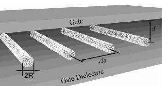
In this letter, we use a model system, illustrated in Fig. 1, consisting of a parallel array of evenly spaced SWNTs fully embedded in a gate dielectric with a planar gate electrode to examine capacitive coupling in SWNT TFTs. The influence of nonuniform intertube spacings is also evaluated to show the applicability of those results to real devices. Results obtained in the single subband quantum limit and those obtained in the classical limit agree qualitatively in the range of dielectric thicknesses and tube densities (as measured in number of tubes per unit length) explored here. The models are used to provide insights into factors that limit the effective mobilities () achievable in these devices.
We begin by calculating of the model system in the quantum limit, where the charge density of the SWNT in the ground state has full circular symmetry.8 In this case, the charge distributes itself uniformly around the tube, and each tube, when tuned to the metallic region, can be treated as a perfectly conducting wire with radius and uniform linear charge density . The electrostatic potential induced by such a perfect conducting wire is: where is the distance away from the center of the wire. The potential generated by an array of such wires is also a linear function of r and in general, the induced potential at the i-th tube depends on of every tube in array according to
| (1) |
where coefficients of inductive coupling between i-th and j-th tube are geometry dependent.9
For SWNTs in the metallic regime, is proportional to the shift of the Fermi level which is itself proportional to an average acting potential at the nanotube according to:
| (2) |
where the proportionality coefficient is the quantum capacitance .8 ; 10 ; 11 This equation is written to separate contributions from the external potential, , as applied by distant electrodes and as generated by any other external source associated with charge traps, interface states, etc, and the induced potential, , as given by Eq. (1).
For the case of a SWNT TFT device, we are interested in a solution that corresponds to the case of a uniform : . Thus, is the same for each tube in the array and can be written as: where is the reciprocal geometric capacitance between a single tube and its n-th neighbor in the given array geometry. The total induced potential is and the total reciprocal capacitance of the tube is the sum of all plus . The exact analytical expressions for and the sum for each tube in a regular array of SWNTs separated by the distance can be derived as,
| (3) |
where is the distance between a given tube and its n-th neighbor. To apply this result to the problem of SWNT TFT we calculate the total charge per unit area induced in the array under :
| (4) |
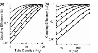
and depends on two characteristic lengths: , which defines the inter-tube coupling, and , which defines the coupling of a single tube to the gate. The physics of coupling is clearly different for two different regimes determined by (assuming that is always the smallest quantity). In the limit (i.e. sparse tube density) the planar gate contribution dominates, , and reduces to that for a single, isolated tube. is approximately equal to the product of the capacitance of a transistor that uses a single isolated SWNT with the number of tubes per screening length . In the opposite limit, , approaches that of a parallel plate primarily due to the higher surface coverage of tubes. Meanwhile, decreases due to the screening by neighboring tubes. To compare the performance of SWNT network/array based TFTs with that of conventional TFTs that uses continuous, planar channels, we calculate the ratio of the capacitance of the SWNT-array to that of a parallel plate (Fig. 2). This capacitance ratio, , is close to unity for :
| (5) |
where is the single tube capacitance. The term in parenthesis is multiplied by the inverse tube density and is, therefore, negligible when the becomes much smaller than . For , in the opposite limit, is small and grows linearly with as given by: .
To verify certain aspects of these calculations, we performed finite-element-method (FEM) electrostatic simulations (FEMLab, Comsol, Inc) to determine the classical of the same model system, in which the induced charge distributes itself to establish an equal potential over the nanotubes. In these calculations, was set to 0.7 nm, which corresponds to the average radius of SWNTs formed by chemical vapor deposition.12 We chose . The computations, shown in Fig. 2, agree qualitatively with those determined by Eq. 4, with deviations that are most significant at small gate dielectric thicknesses where quantum effects are significant.
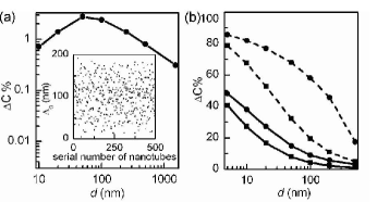
In experimentally achievable SWNT TFTs, the SWNTs are not spaced equally and, except in certain cases, they are completely disordered in the form of random networks.5 ; 13 To estimate qualitatively the influence of uneven spacings, we constructed an array composed of five hundred parallel SWNTs with a normal distribution of nm (Fig. 3a inset). was calculated by inverting the matrix of potential coefficients (Eq. 1). The small difference of computed capacitances () indicates that Eq.4 can be used for aligned arrays with uneven spacings, and perhaps even random SWNT networks (Fig. 3). Another experimental fact is that most SWNT TFTs are constructed in the bottom-gate structure where nanotubes are in an equilibrium distance above the gate dielectric, Å,14 due to van der Waals interactions. To account for the effect of low air medium on , we performed the FEM simulation for nanotube arrays either fully embedded in gate dielectric or fully exposed in the air. Comparing the capacitances in these two cases shows that the low air medium has most significant influence on those systems that use high dielectrics because of the higher dielectric contrast. Moreover, at the effect of the air on SWNT arrays is close to results obtained for devices based on individual tubes (Fig.3 b).15 However, with increasing , the screening between neighboring tubes forces electric field lines to terminate on the bottom of nanotubes without fringing through the air and thus the air effect diminishes.
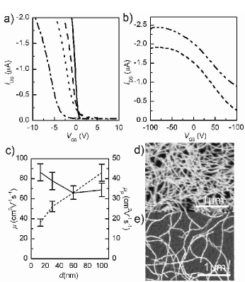
To explore these effects experimentally, we built TFTs that used random networks of SWNT with fixed (approximately 10 tubes/micron, as evaluated by AFM) and different . Details on the device fabrication can be found elsewhere.16 For the range of and here the difference in that results from the air effect is less than 20%, smaller than the experimental error in determining transconductance (). So, Eq.4 gives sufficiently accurate estimation of . Figure 4a shows the transfer curves of SWNT TFTs. Figure 4c compares effective mobilites calculated using derived from parallel plate model () to those that from Eq.4 (). Consistent with the previous discussion, the parallel-plate capacitor model overestimates significantly for low tube densities/thin dielectrics. As a result, the effective mobilities calculated in this manner () have an apparent linear dependence on that derives from inaccurate values for . On the other hand, effective mobilities calculated using Eq.4 () show no systematic change with , which provides a validation of the model.
The computed capacitances also reveal two important guidelines for the development of SWNT TFTs. First, Eq.3 and Eq.4, indicate that the effective should be close to the intrinsic mobility of SWNTs () if the contact resistance is neglected since
| (6) |
where is the total number of effective pathways, connecting source/drain electrodes. can be a little smaller than because the actual length of effective pathway is longer than . The huge difference between of devices based on SWNT films5 ; 6 ; 13 and extracted from those FETs based on individual tubes17 suggests that the tube/tube contacts severely limit the transport in SWNT networks or partially aligned arrays, either due to tunneling barrier or electrostatic screening at the contact which prevents the effective gate modulation at that specific point.18 Secondly, efforts on improving through increasing tube density for a given device geometry and are limited by . From Fig. 2a we can see that at given , when , , and thus increases with the increase of tube density. However, when , saturates and no longer increases with decreasing . This prediction was verified by the almost identical for devices with different tube densities on thick gate dielectric (Fig. 4b).
In summary, we evaluated of SWNT TFTs. Our analysis shows that the best electrostatic coupling between the gate and the SWNT occurs in dense arrays of tubes, but advantage gained in coupling from higher tube density starts to saturate as becoming close to . These conclusions are corroborated by vertical scaling experiments on SWNT network TFTs. We further propose two guidelines for improving the performance of SWNT TFTs.
ACKNOWLEDGEMENTS
We thank T. Banks for help with the processing. This work was supported by the U. S. Department of Energy under grant DEFG02-91-ER45439 and the NSF through grant NIRT-0403489.
References
- (1) Q. Cao, C. Kocabas, M. A. Meitl, S. J. Kang, J. U. Park, and J. A. Rogers, in Carbon Nanotube Electronics, edited by A. Javey and J. Kong (Springer Verlag GmbH Co., KG, 2007).
- (2) C. Kocabas, M. Shim, and J. A. Rogers, J. Am. Chem. Soc. 128, 4540-4541 (2006).
- (3) Q. Cao, S.-H. Hur, Z.-T. Zhu, Y. Sun, C. Wang, M. A. Meitl, M. Shim, and J. A. Rogers, Adv. Mater. 18, 304- 309 (2006).
- (4) K. Bradley, J. C. P. Gabriel, and G. Gr ner, Nano Lett. 3, 1353-1355 (2003).
- (5) E. S. Snow, P. M. Campbell, M. G. Ancona, and J. P. Novak, Appl. Phys. Lett. 86, 033105 (2005).
- (6) S.-H. Hur, C. Kocabas, A. Gaur, M. Shim, O. O. Park, and J. A. Rogers, J. Apply. Phys. 98, 114302 (2005).
- (7) J. Guo, S. Goasguen, M. Lundstrom, and S. Datta, Appl. Phys. Lett. 81, 1486-1488 (2002).
- (8) S. V. Rotkin, in Applied Physics of Nanotubes, edited by Ph. Avouris (Springer Verlag GmbH Co., KG, 2005).
- (9) S. V. Rotkin, unpublished results.
- (10) K. A. Bulashevich and S. V. Rotkin, JETP Lett. 75, 205- 209 (2002).
- (11) S. Rosenblatt, Y. Yaish, J. Park, J. Gore, V. Sazonova, and P. L. McEuen, Nano Lett. 2, 869-872 (2002).
- (12) Y. Li, W. Kim, Y. Zhang, M. Rolandi, D. Wang, and H. Dai, J. Phys. Chem. B 105, 11424 - 11431 (2001).
- (13) C. Kocabas, S. H. Hur, A. Gaur, M. A. Meitl, M. Shim, and J. A. Rogers, Small 1, 1110-1116 (2005).
- (14) D. Qian, G. J. Wagner, W. K. Liu, M.-F. Yu, and R. S. Ruoff, Appl. Mech. Rev. 55, 495-532 (2002).
- (15) O. Wunnicke, Appl. Phys. Lett. 89, 083102 (2006).
- (16) Q. Cao, M.-G. Xia, M. Shim, and J. A. Rogers, Adv. Func. Mater. in press (2006).
- (17) X. J. Zhou, J. Y. Park, S. M. Huang, J. Liu, and P. L. McEuen, Phys. Rev. Lett. 95, 146805 (2005).
- (18) A. A. Odintsov, Phys. Rev. Lett. 85, 150-153 (2000).
- (19) S. J. Kang, C. Kocabas, T. Ozel, M. Shim, S. V. Rotkin, and J. A. Rogers, unpublished results (2006).


