Optical and electrical spin injection and spin transport in hybrid Fe/GaAs devices
Abstract
We discuss methods for imaging the nonequilibrium spin polarization of electrons in Fe/GaAs spin transport devices. Both optically- and electrically-injected spin distributions are studied by scanning magneto-optical Kerr rotation microscopy. Related methods are used to demonstrate electrical spin detection of optically-injected spin polarized currents. Dynamical properties of spin transport are inferred from studies based on the Hanle effect, and the influence of strain on spin transport data in these devices is discussed.
The demonstration of electrical spin injection and spin detection in lateral metallic devices, including spin-valve and spin precession effects Johnson ; Jedema ; Valenzuela , has generated considerable interest in related devices based on semiconductors. Unlike their metallic counterparts, characterization of these ‘semiconductor spintronic’ structures benefits from the many magneto-optical tools that have been developed over the years to probe spin-polarized electrons and holes in semiconductors OO . In this paper we describe experiments that measure and image both optically- and electrically-injected spin polarizations in GaAs using scanning magneto-optical Kerr rotation microscopy. These techniques are applied to hybrid Fe/GaAs lateral spin transport structures. Using cw lasers and small magnetic fields to induce electron spin precession, dynamical properties of spin transport are inferred from Hanle-effect studies and theoretical models of the spin drift-diffusion equations. The influence of strain on spin transport measurements is also discussed. Related techniques are used to demonstrate electrical spin detection of optically-injected spin polarized currents in these devices.
Figure 1 shows a schematic of the experiment. The Fe/GaAs devices are mounted, nominally strain-free, on the variable-temperature cold finger of a small optical cryostat (all presented data were acquired at 4 K). The cryostat itself is mounted on a x-y stage. The samples may also be held by a small cryogenic vise machined into the cold finger CrookerPRL . The uniaxial stress applied to the sample by the vise is uniform and can be varied in situ by a retractable actuator. For devices grown on [001] oriented GaAs substrates and cleaved along the usual crystal axes, this uniaxial (shear) stress leads to nonzero off-diagonal elements of the crystallographic strain tensor in GaAs, . couples directly to electron spin () and momentum (k) via spin-orbit coupling, leading to effective magnetic fields ‘seen’ by moving electrons OO ; CrookerPRL .
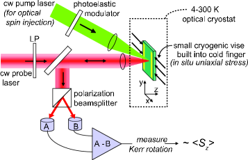
The steady-state spin polarization of conduction electrons in the GaAs is measured by the polar magneto-optical Kerr effect. As has been briefly described in recent works CrookerPRL ; CrookerScience ; Hruska ; Furis , a cw probe laser beam, derived from a narrowband and frequency tunable Ti:sapphire ring laser, is linearly polarized and focused tightly to a 4 m spot on the sample. The Kerr rotation (i.e., optical polarization rotation) imparted to the reflected probe laser is proportional to the out-of-plane () component of electron spin, . This Kerr rotation (KR) is measured by balanced photodiodes using lock-in techniques. To measure optically-injected spins, a 1.58 eV cw pump laser is also focused to a 4 m spot on the device. The polarization of this pump laser is modulated from left- to right- circular (injecting spins oriented along ) by a 50 kHz photoelastic modulator. To measure electrically-injected spins, the electrical bias applied to the Fe contacts is square-wave modulated at 3.1 kHz. The cryostat and/or the probe laser can be raster-scanned in the x-y plane to acquire a 2D image of the electron spin polarization . We simultaneously image the reflected probe intensity to infer the topography of the device surface. The applied magnetic field is controlled by external coils.
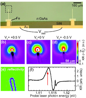
Figure 2(a) shows a photomicrograph of a Fe/GaAs “finger” device. All devices were fabricated from Fe/GaAs heterostructures grown by molecular beam epitaxy as described in Refs. CrookerScience ; XiaohuaPRL . Briefly: on (001) oriented semi-insulating GaAs, 300 nm of undoped GaAs was grown, followed by a 2 m epilayer of Si-doped n:GaAs having electron doping in the range /cm3 to maximize the low-temperature electron spin lifetime and spin transport length Kikkawa ; DzhioevPRB ; Furis . Then a 15 nm layer was grown where the doping was rapidly increased to /cm3, followed by a 15 nm layer doped uniformly at /cm3. These heavily-doped layers define a narrow Schottky barrier through which electrons can tunnel Hanbicki . Then 5 nm of Fe was epitaxially deposited, followed by 2 nm of Al. To define the lateral structures, the metal and :GaAs were etched away except for the Fe contact regions. Gold contacts were deposited after a SiN insulation layer.
The images in Figs. 2(b-d) show the drift and diffusion of optically injected electron spin polarization in the vicinity of one Fe finger (dotted region in Fig. 2(a)). Spins are optically injected just off the tip of the left Fe finger, and the dc electrical bias applied to this Fe finger (relative to the rightmost Fe finger) is , 0, and -0.5 V respectively. At zero bias, the spins diffuse radially away from the point of injection with a spin diffusion length of order 10 m. At positive (negative) bias, these optically injected spins are directly observed to flow into (away from) the Fe finger, which is acting as a drain (source) of electron current. The reflectivity image of Fig. 2(e) shows the border of the Fe finger.
These Kerr images were acquired with the probe laser tuned to a photon energy of 1.513 eV, just below the bandgap of the n:GaAs. The optical KR that is due to the presence of spin-polarized electrons in the n:GaAs is strongly dependent on photon energy, and its explicit dependence in this device is shown in Fig. 2(f). The exact shape of this curve varies from device to device, and depends in part on the thickness and doping density of the n:GaAs layer. Further, once this sample-specific and spin-dependent ‘fingerprint’ is established, spectral shifts of this curve provide a sensitive and quantitative measure of strain (intentional or otherwise) in the sample CrookerPRL . The shape and sign of this curve can change if the probe laser is positioned over other features on the device such as the Fe contacts. For example, at this probe energy of 1.513 eV, the spin polarized electrons that have diffused under the Fe contacts in Figs. 2(b-d) lead to a KR of opposite sign (black regions in the images; see color scale). This can also be observed in Figs. 4 and 5.
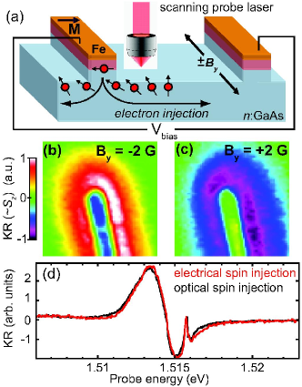
Figure 3 shows measurements of this same device for the case of electrical spin injection. Fig. 3(a) sketches the experiment, wherein a voltage bias is applied across the two Fe fingers. Spin-polarized electrons at the Fermi level of the Fe tunnel through the thin Schottky barrier defined by the :GaAs region and into the n:GaAs epilayer. The initial spin polarization of these injected electrons is in-plane and antiparallel to the Fe magnetization M (corresponding to majority spins in Fe CrookerScience ). A small magnetic field, also in-plane but orthogonal to , is used to precess these injected spins to the out-of-plane direction () so that they can be measured by the polar Kerr effect. Figs. 3(b) and (c) show images of the electrically injected spin polarization, where the injected spins are tipped into the and direction by a positive and negative in-plane magnetic field.
We confirm that these electrically-injected spins induce the same KR spectral ‘fingerprint’ as for the previous case of optically-injected spins in this device. With the probe laser positioned on the n:GaAs near the Fe finger, the KR was measured versus probe energy for both positive and negative in-plane magnetic field. The red line in Fig. 3(d) shows the difference of these two curves, which eliminates any field-independent birefringent offsets that can arise from electrical modulation, and leaves behind only the signal that depends on electron spin precession. This purely spin-dependent signal agrees very well within an overall scale factor with the previous KR signal resulting from optical spin injection (black curve).
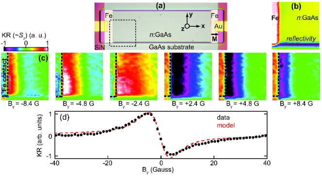
Figure 4(a) shows one of a later series of spin transport devices having rectangular Fe/GaAs source and drain contacts at either end of a long n:GaAs channel. Studies of electrical spin injection, accumulation and transport in these devices were reported in Ref. CrookerScience , and all-electrical detection of spin accumulation was reported in Ref. XiaohuaPRL . In Fig. 4 we show the effect of in-plane magnetic fields on images of electrically-injected spins. We image an m region that includes part of the Fe injection contact and the bottom edge of the n:GaAs channel (dotted square in Fig. 4(a)). A reflectivity image (see Fig. 4b) clearly shows these features. With V, Fig. 4(c) shows a series of KR images of the electrically-injected spins as is varied from -8.4 G to +8.4 G. Injected electrons, spin polarized initially along the direction, precess into the or direction when is oriented along or . These injected electrons flow down the channel with average drift velocity that is the same in all the images. The drifting spins precess at a rate proportional to ; thus, the spatial period of the observed spin precession is short when is large.
This series of images helps to make clear why, when the probe laser is fixed at a point in the n:GaAs channel and is measured as an explicit function of , we obtain “Hanle curves” having the characteristic antisymmetric lineshape shown in Fig. 4(d). The detailed structure of these Hanle curves (i.e., their amplitudes, half-widths, and oscillations) contains considerable information about the dynamics of electron spin transport in these devices including spin lifetime , diffusion constant and drift velocity CrookerScience ; Hruska . For the effectively one-dimensional spin transport realized in this device, an analytic integral solution to the spin drift-diffusion equations is readily derived CrookerScience and these Hanle curves can be accurately modeled (see dotted red line). We verify also that these curves invert when the magnetization M of the Fe contacts is intentionally reversed (compare, e.g., with the Hanle curves in Fig. 5), and confirm that M is not affected by .
Imaging studies also reveal a region of spin accumulation in the n:GaAs channel near the Fe drain contact. Spin accumulation in these devices results from spin-dependent transmission and reflection of electrons at the Fe/GaAs tunnel barrier and was studied in detail in Ref. CrookerScience , and was also investigated in forward-biased MnAs/GaAs structures by Stephens et al Stephens .
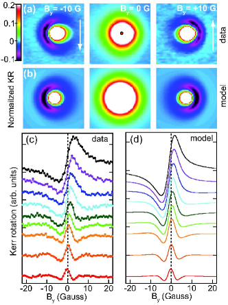
Figure 5 shows how we detect the presence of off-diagonal strain, , in these devices, and shows also how manifests in spin transport studies. The device is the same as that shown in Fig. 4 and – in this case – the strain was inadvertent, resulting most likely from improper mounting and cooldown of the device. Figure 5(a) shows images of spin-polarized electrons, optically injected in the middle of the n:GaAs channel, diffusing radially away from the point of injection. The applied magnetic field in the three images is , 0, and +10 G respectively (see white arrows). The images are clearly asymmetric in the presence of , and this asymmetry inverts when reverses. This asymmetry provides direct evidence for the presence of off-diagonal strain in this device, and arises from the asymmetric net magnetic field ‘seen’ by the electrons, which are diffusing along all momentum directions k in the x-y plane. The net field is the vector sum of both the applied magnetic field and a k-dependent effective magnetic field that is due to spin-orbit coupling to strain OO ; CrookerPRL : . describes an effective field that is always in-plane and orthogonal to k, and is oriented along for spins diffusing to the right or left. When is negative (in Fig. 5(a)), electron spins diffusing to the left ‘see’ a large net magnetic field and precess (giving negative KR), while spins diffusing to the right see little or no net field ( and oppose each other) and do not precess, resulting in an asymmetric image. Carefully remounting the sample eliminated this accidental strain, and subsequent images in the presence of revealed a symmetric annulus of negative KR, as expected. Other methods to detect strain and its influence on electron spins have also been demonstrated, for example, based on the shift of photoluminescence Hanle curves with the device under electrical bias Korenev , or on time-resolved precession of flowing electrons in zero magnetic field KatoNature .
These asymmetric KR images can be modeled by numerically solving a set of strain-dependent spin-drift-diffusion equations, derived in Refs. CrookerPRL ; Hruska . Figure 5(b) shows modeled data using known sample parameters and a small off-diagonal strain: . Note this strain is over two orders of magnitude smaller than typical strains associated with, for example, biaxial strain due to lattice-mismatched growth. These images thus provide a sensitive diagnostic to quantify the presence of in these devices, particularly when is large.
Despite the small value of inferred from the images of Fig. 5(a), this strain manifests directly in studies of electrically-injected spin transport. Figure 5(c) shows Hanle curves ( versus ) acquired in the n:GaAs channel of this device, at increasing distances from the Fe/GaAs source contact. Near the source contact (black curve, 2 m away), is an odd function of , as expected and as discussed above. Moving down the n:GaAs channel, the curves become narrower (reflecting the increasing ‘age’ of the measured electrons CrookerScience ) and, more importantly, they shift to the left. At a distance of 42 m from the source contact, has become an even function (red curve). This shift is due to the presence of and its associated , which augments for electrons flowing down the channel. Again, these Hanle curves can be modeled by numerically solving the spin-drift-diffusion equations in the presence of strain. Figure 5(d) shows the modeled data, again using .
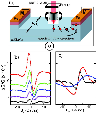
It was also demonstrated in Ref. CrookerScience that these Fe/GaAs Schottky tunnel barriers can function as electrical spin detectors in addition to their role as spin injectors. To demonstrate spin-dependent conductivity through a Fe/GaAs contact, we use the experimental geometry sketched in Fig. 6(a). We optically inject spin polarized electrons into the n:GaAs channel using the circularly polarized pump laser. By current-biasing the device, we cause these spins to flow to and through the Fe/GaAs drain contact. The spin polarization of this current at the drain contact can be tipped parallel or antiparallel to the Fe magnetization M using a small magnetic field . We measure the device conductance, , as a function of . This experiment is the inverse of the Kerr-effect measurements described in the first part of this paper: Instead of optically measuring the component of drifting spins that are electrically injected along , here we electrically measure the component of drifting spins that are optically injected along . The drift-diffusion equations apply equally, and therefore has the same characteristic antisymmetric “Hanle curve” shape. Figure 6(b) shows the normalized conductance change versus for spins that were optically injected 40 m “upstream” from the edge of the Fe/GaAs drain contact, for varying pump powers. The conductance change between spins oriented parallel or antiparallel to M is not large – of order one part in – but the signal-to-noise ratio measured in this way is nonetheless excellent. Lastly, Fig. 6(c) shows versus at three different current biases for spins optically injected 25 m from the drain. At low current the curves are narrow (black), reflecting the long time required for spins to drift from the point of injection to the drain contact. At high current bias the spins drift quickly to the drain and the curve is correspondingly much broader, as expected (blue curve). The data in Fig. 6(c) are inverted compared to Fig. 6(b), reflecting the fact that the magnetization M of the drain contact was reversed between these two data sets. In this device, the conductance is largest when the electron current flowing through the drain is spin polarized parallel to M.
In conclusion we have discussed methods, based on the magneto-optical Kerr effect, to study and image both optically- and electrically-injected spin polarizations in GaAs. These measurements help to characterize spin transport phenomena in lateral Fe/GaAs devices and suggest routes for all-electrical studies of spin-dependent transport in hybrid ferromagnet-semiconductor structures. This work was supported by the DARPA SpinS and Los Alamos LDRD programs, the NSF MRSEC program under grant DMR 02-12302, the Office of Naval Research, and the Minnesota Nanofabrication Center, which is supported by the NSF NNIN program.
References
- (1) M. Johnson and R. H. Silsbee, Phys. Rev. Lett. 55, 1790 (1985).
- (2) F. J. Jedema, H. B. Heersche, A. T. Filip, J. J. A. Baselmans, B. J. van Wees, Nature 416, 713 (2002).
- (3) S. O. Valenzuela and M. Tinkham, Nature 442, 177 (2006).
- (4) G. E. Pikus and A. N. Titkov, in Optical Orientation, F. Meier and B. P. Zakharchenya, Eds. (North-Holland, Amsterdam,1984), pp. 73-131.
- (5) S. A. Crooker and D. L. Smith, Phys. Rev. Lett. 94, 236601 (2005).
- (6) S. A. Crooker, M. Furis, X. Lou, C. Adelmann, D. L. Smith, C. J. Palmstrøm, and P. A. Crowell, Science 309, 2191 (2005).
- (7) M. Hruška, S. Kos, S. A. Crooker, A. Saxena, and D. L. Smith, Phys. Rev. B 73, 075306 (2006).
- (8) M. Furis, D. L. Smith, J. L. Reno, and S. A. Crooker, Appl. Phys. Lett. 89, 102102 (2006).
- (9) X. Lou, C. Adelmann, M. Furis, S. A. Crooker, C. J. Palmstrøm, and P. A. Crowell, Phys. Rev. Lett. 96, 176603 (2006).
- (10) J. M. Kikkawa and D. D. Awschalom, Nature 397, 139 (1999).
- (11) R. I. Dzhioev et al., Phys. Rev. B 66, 245204 (2002).
- (12) A. T. Hanbicki et al, Appl. Phys. Lett. 82, 4092 (2003).
- (13) J. Stephens, J. Berezovsky, J. P. McGuire, L. J. Sham, A. C. Gossard, D. D. Awschalom, Phys. Rev. Lett. 93, 097602 (2004).
- (14) V. K. Kalevich and V. L. Korenev, JETP Lett. 52, 230 (1990).
- (15) Y. Kato, R. C. Myers, A. C. Gossard, and D. D. Awschalom, Nature 427, 50 (2004).