Generation of dc spin current in a narrow channel with Rashba and Dresselhaus spin-orbit interaction
Abstract
We consider a finite range ac-biased front gate acting upon a quantum channel with Rashba and Dresselhaus spin-orbit interaction effects. The ac-biased gate, giving rise to a dynamical Rashba coupling, causes spin-resolved coherent resonant inelastic scattering. A pure dc spin current is subsequently generated without accompanying charge current. In the presence of Dresselhaus effect, the dc spin current is suppressed in the low kinetic energy regime but is assisted in the high kinetic energy regime.
pacs:
73.23.-b, 72.23.Ad, 72.25.Dc, 72.30.+qManipulation of electron spins is achievable with external active control, which is a central requirement of spintronic devices. Of fundamental interest and practical application is the spin current in the emerging field of spintronics.Awschalom02 One of the key issues is how to generate spin current in spintronic devices. The standard way is to inject spin polarized current from a ferromagnetic electrode.Wolf01 However, its efficiency is usually limited by the poor quality of the interface, and it is accompanied by the charge current. Narrow gap semiconductor heterostructures offer an efficient control of spins through intrinsic spin-orbit interaction (SOI). Several approaches utilizing spin Hall effects,Murakami03 ; Kato04 ; Sinova04 ; Bernevig06 ; Valenzuela06 ; Sih06 magnetic fields,Muccio02 ; Brataas02 ; Zhang03 ; Wang03 ferromagnetic materials,Sun03 ; Zeng03 or optical excitationsBhat00 ; Hubner03 ; Stevens03 were proposed.
The success of dc front-gate control for the measurementNitta97 of Rashba coupling strength,Rashba60 inspired proposals for spin current generation by nonmagnetic means.Pras03 ; Governale03 ; Malsh03 ; Tang05 ; Wang06 These proposals include adiabatic quantum pumping in a quantum dot with static SOIPras03 interfaced with a time-dependent barrier and a spatially separated Rashba SOI region,Governale03 and an ac-biased Rashba-type two-dimensional (2D) disorder systemTang05 or quantum channel.Wang06 It is known that the translational invariance is broken in the channel direction due to a spatially localized time-dependent potential, thus allowing us to explore coherent resonant inelastic scattering and time-modulated quasi-bound state features.Tang96
In addition to the Rashba SOI,Rashba60 which is caused by the structure inversion asymmetry (SIA) of the confining potential of the 2D trapping well, there is also a Dresselhaus effectDresselhaus55 caused by the bulk inversion asymmetry (BIA)Dyakonov86 and the interface inversion asymmetry (IIA).Vervoort97 The contributions associated with BIA and IIA are phenomenologically inseparable. The Rashba effect is usually dominant, but the Dresselhaus effect could be also observable.Ganichev04 In this paper, we consider a narrow channel formed in a high-mobility electronic quantum well by applying negative bias on the front split gates. When a finger gate is deposited above the split gate separated by an insulating layer, a local time varying Rashba coupling parameter can be induced by ac-biasing the finger gate.Governale03 ; Wang06 We shall explore how the interplay among the static Rashba, the static Dresselhaus, and the dynamical Rashba SOI effects influences the efficiency of spin current generation in the absence of source-drain bias.
The electron transport in a narrow channel in the presence of SOI can be described by the dimensionless HamiltonianTang96
| (1) |
where the first term denotes the kinetic energy and the third term is a potential that confines the electron in the direction. For a narrow quantum well along [0,0,1] crystallographic direction, the unperturbed SOI term involving Rashba and Dresselhaus interaction effects can be described in terms of -linear form
| (2) | |||||
where ( = {}) are the Pauli matrices and is the 2D electron wave vector. The unperturbed Rashba coupling strength is proportional to the electric field along direction perpendicular to the 2D electron gas. Moreover, the Dresselhaus coupling strength is determined by the semiconductor material and the geometry of the sample.
For a narrow wire,Pereira05 the spin-orbit coupling contributions can be simplified as . The right-going (left-going) eigenfunctions of the unperturbed Hamiltonian in the subband are given by
| (3) |
where labels the two spin branches, is the spinor of branch with two components given by and with . In addition, the wave vectors are defined by and , where is the chemical potential, , and is the subband threshold, which is shifted from the bare subband bottom by . The total Hamiltonian contains a dynamical term, induced by the ac-biased finger gate, which can be written in the form
| (4) |
where is the step function and {,} stands for anti-commutator.
The scattering wave function of the conduction electron incident from the left reservoir in the spin state can be obtained of the form . In the region , the time-dependent wave function along the channel direction is given by
| (5) |
where and denotes the reflection coefficient of the conduction electron in the subband and photon sideband . In the region , the wave function is simply of the form
| (6) |
where indicates the corresponding transmission coefficient. The longitudinal wave function in the time-modulated region is given byTang96
| (7) | |||||
where if is even, and if is odd. Performing the time-dependent mode matching at ,Wang06 one can obtain the reflection and transmission coefficients, and , at the edges of the time-modulated region. Similarly, it is easy to obtain and for the conduction electrons incident from the right reservoir.
Summing over all possible scattered propagating modes from both reservoirs, the net right-going dc spin current can be expressed as , where
| (8) |
with being the Fermi function in the reservoirs. In addition, and , where . The spin current conservation is maintained due to the suppression of spin-flip subband mixing. Since a symmetric marrow channel configuration gives , the net charge current is identically zero, and a pure nonequilibrium spin current is generated.
The calculations presented below are carried out under the assumption that the electron effective mass , which is appropriate to the InGaAs-InAlAs interface. The typical electron density cm-2 and eV m.Nitta97 We select such that the subband level spacing, , is 4.13 meV. Accordingly, the length unit nm, the energy unit meV, and the spin-orbit coupling parameters are in units of m/s.
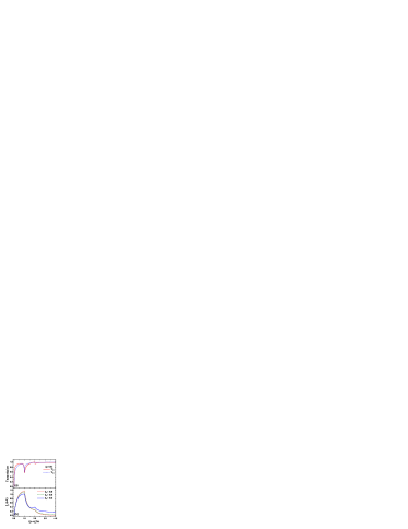
In Fig. 1, we demonstrate how the Dresselhaus spin-orbit coupling strength influence the dc spin current generated by the ac-biased front gate with driving region nm. The other parameters are static Rashba parameter eV m, , and meV. In Fig. 1(a), we see that since in the low kinetic energy regime (), and hence positive spin current is generated. On the other hand, the sharp dip structure at is the one-photon quasibound-state feature.Tang96 For electron energies at , we see clearly leading to positive spin current. The change in sign in the transmission difference across the dip structures, that is, while . Consequently, for electrons with incident energy , the spin current peak is generated with the order of 1 nA, as is shown in Fig. 1(b).
For the cases of zero and weak Dresselhaus SOI such as and , the electrons with energy exhibit small dip structures which is associated with two-photon quasibound-state feature. Since at the current transmission of spin- electron is still less than of the spin- electron, there is no significant contribution to the generation of dc spin current. In Fig. 1(a), we show the current transmission for the case of strong Dresselhaus coupling . The right-going spin- electron manifests Fano-type peak-and-dip line shape in transmission at , which is associated with the two-photon quasibound-state feature. This Fano-type feature enhances to be greater than . Consequently, the pumped dc spin current is thus significantly enhanced.
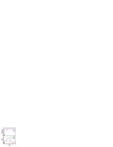
Figure 2 shows the spin-resolved transmission with dynamical Rashba coefficient and the generated dc spin current for cases of , , and . The other parameters are: ac-driven region nm, Rashba strength eV m, Dresselhaus strength , and driving frequency GHz. There are common transport features for the three different dynamical coupling strngth. The overlap of curves for the incident electron energies implies the transport properties is insensitive to the driving strength in the very low kinetic energy regime. The similar plateau features in at are caused by the competition of the current transmission of spin- and spin- electrons.
At incident electron energy , there are kink structure in for , peak structure for , and shoulder structure for . For the case of , the current transmission of the two spin states are almost the same at exhibiting plateau feature while the transmission of the spin- electron is smaller than the spin- at exhibiting strong drop feature in . For the case of , the crossover in the transmission for two spin states leads to the peak structure at . However, for the case of , we see that is greater than until the crossover at leading to the shoulder behavior in . This feature in combination with the broad dip structure, associated with electrons emitting two photons to the subband threshold forming a quasibound state, results in the broad spin current peak nA at . Small hill in at is barely recognized. At , the spin currents are nearly saturated to , , and nA for , , and , respectively.
In this paper we have investigated non-adiabatically how the dc spin current is generated under the mechanism of SOI using a dynamical all electrical control on a split-gate-confined narrow channel. We have demonstrated nontrivial features concerning the spin current generation mechanism caused by different strength of Dresselhaus spin-orbit coupling. These results provide a robust manner of generating spin current without accompanying charge current.
The spin current generating features have been demonstrated and illustrated in detail. It has been found that the Dresselhaus spin-orbit coupling intends to suppress the efficiency of spin current generation in the low kinetic energy regime, while the Dresselhaus effect can enhance the pumped spin current in the high kinetic energy regime. Unlike the parametric quantum pumping, in which two pumping potentials with a phase difference is needed.Muccio02 Our proposed spin current generating device is achievable using a single ac-biased gate, and should be achievable within recent fabrication capability.
The authors acknowledge the financial support by the National Science Council and the Academia Sinica in Taiwan. C.S.T. is grateful to inspiring discussions with L.Y. Wang and C.S. Chu, and the computational facility supported by the National Center for High-Performance Computing of Taiwan.
References
- (1) Semiconductor Spintronics and Quantum Computation, edited by D.D. Awschalom, N. Samarth, and D. Loss (Springer-Verlag, Berlin, 2002).
- (2) S. A. Wolf et al., Science 294, 1488 (2001).
- (3) S. Murakami, N. Nagaosa, and S. C. Zhang, Science 301, 1348 (2003).
- (4) Y. K. Kato, R. C. Myers, A. C. Gossard, D. D. Awschalom, Sceince 306, 1910 (2004).
- (5) J. Sinova et al., Phys. Rev. Lett. 92, 126603 (2004); J. Wunderlich et al., ibid. 94, 047204 (2005).
- (6) B. A. Bernevig and S. C. Zhang, Phys. Rev. Lett. 96, 106802 (2006).
- (7) S. O. Valenzuela and M. Timkham, Nature 442, 176 (2006).
- (8) V. Sih, W. H. Lau, R. C. Myers, V. R. Horowitz, A. C. Gossard, and D. D. Awschalom, Phys. Rev. Lett. 97, 096605 (2006); N. P. Stern, S. Ghosh, G. Xiang, M. Zhu, N. Smarth, D. D. Awschalom, ibid. 97, 126603 (2006).
- (9) E. R. Mucciolo, C. Chamon, and C. M. Marcus, Phys. Rev. Lett. 89, 146802 (2002); S. K. Watson, R. M. Potok, C. M. Marcus, and V. Umansky, ibid. 91, 258301 (2003).
- (10) A. Brataas, Y. Tserkovnyak, G. E. W. Bauer, and B. I. Halperin, Phys. Rev. B 66, 60404 (2002).
- (11) P. Zhang, Q. K. Xue, and X. C. Xie, Phys. Rev. Lett. 91, 196602 (2003).
- (12) B. G. Wang, J. Wang, and H. Guo, Phys. Rev. B 67, 092408 (2003).
- (13) Q. F. Sun, H. Guo, and J. Wang, Phys. Rev. Lett. 90, 258301 (2003).
- (14) W. Zeng, J. L. Wu, B. G. Wang, J. Wang, Q. F. Sun, and H. Guo, Phys. Rev. B 68, 113306 (2003).
- (15) R. D. R. Bhat and J. E. Sipe, Phys. Rev. Lett. 85, 5432 (2000).
- (16) J. Hubner, W. W. Ruhle, M. Klude, D. Hommel, R. D. R. Bhat, J. E. Sipe, and H. M. van Driel, Phys. Rev. Lett. 90, 216601 (2003).
- (17) M. J. Stevens, A. L. Smirl, R. D. R. Bhat, A. Najmaie, J. E. Sipe, and H. M. van Driel, Phys. Rev. Lett. 90, 136603 (2003).
- (18) J. Nitta, T. Akazaki, H. Takayanagi, and T. Enoki, Phys. Rev. Lett. 78, 1335 (1997); D. Grundler, ibid. 84, 6074 (2000).
- (19) E. I. Rashba, Sov. Phys. Solid State 2, 1109 (1960); Y. A. Bychkov and E. I. Rashba, J. Phys. C 17, 6039 (1984).
- (20) P. Sharma and P. W. Brouwer, Phys. Rev. Lett. 91, 166801 (2003).
- (21) M. Governale, F. Taddei, and R. Fazio, Phys. Rev. B 68, 155324 (2003).
- (22) A. G. Mal’shukov, C. S. Tang, C. S. Chu, and K. A. Chao, Phys. Rev. B 68, 233307 (2003).
- (23) C. S. Tang, A. G. Mal’shukov, and K. A. Chao, Phys. Rev. B 71, 195314 (2005); A brief review see C. S. Tang, Int. J. Mod. Phys. 20, 869 (2006).
- (24) L. Y. Wang, C. S. Tang, and C. S. Chu, Phys. Rev. B 73, 085304 (2006).
- (25) C. S. Tang and C. S. Chu, Phys. Rev. B 53, 4838 (1996); C. S. Tang and C. S. Chu, ibid. 60, 1830 (1999); C. S. Tang, Y. H. Tan, and C. S. Chu, ibid. 67, 205324 (2003).
- (26) G. Dresselhaus, Phys. Rev. 100, 580 (1955).
- (27) M. I. D’yakonov and V. Yu. Kachorovskii, Fiz. Tekh. Poluprovodn. 20, 178 (1986) [Sov. Phys. Semicond. 20, 110 (1986)].
- (28) L. Vervoort and P. Voisin, Phys. Rev. B 56, 12744 (1997).
- (29) S. D. Ganichev et al., Phys. Rev. Lett. 92, 256601 (2004).
- (30) R. G. Pereira and E. Miranda, Phys. Rev. B 71, 085318 (2005).