Ferroelectric switched all-metallic-oxide - junctions
Abstract
We report the first formation of the metallic - junctions, the ferroelectric (Ba,Sr)TiO3 (BST) switched optimally electron-doped (-type) metallic T’-phase superconductor, (La,Ce)2CuO4 (LCCO), and hole-doped (-type) metallic CMR manganite (La,Sr)MnO3 (LSMO) junctions. In contrast with the previous semiconductor - (--) junctions which are switched by the built-in field , the present metallic oxides -- junctions are switched by double barrier fields, the built-in field , and the ferroelectric reversed polarized field , both take together to lead the junctions to possess definite parameters, such as definite negligible reversed current ( A), large breakdown voltage (7 V), and ultrahigh rectification () in the bias voltage 1.2 V to 2.0 V and temperature range from 5 to over 300 K. The related transport feature, barrier size effect, and temperature effect are also observed and defined.
pacs:
85.50.-n, 73.40.-c, 73.40.Ei, 74.78.FkFollowing the semiconductor technology, for which the - junctions are the basic devices, the oxide electronics, such as the high- superconductor (HTSC) electronics, spintronics based on the colossal magnetoresistance (CMR) manganites, and so on, the oxide - (--) junctions (oxide diodes) also are the basic devices, and have been studied widely. One route, a hole-doped oxide(s), currently, the -type CMR manganite(s) is used, which is deposited on the -type semiconductor oxide to form the - junctions Tanaka_88_027204_PRL ; Tiwari_APL_83_1773 ; Hu_APL_83_1867 ; Lu_APL_86_2502 ; Xi_APL_61_2353 ; Ramadan_JAP_99_43906 . The other route, the oxide insulator is used to sandwich the semiconductor -type oxide and semiconductor -type oxide (or -type pure semiconductor) to prepare the -- junctions Sugiura_JAP_90_187 ; Mitra_APL_79_2408 ; Lang_APL_87_3502 . It must be noted that the semiconductor functional oxides are usually due to the under doping ,the optimally doped - and -type oxide functional materials are metallic phase oxides with their maximum functions. Therefore, for really developing the oxide electronics and making matchable oxide electronic circuits, exploiting a way to prepare entire new oxide - junctions based on the optimally doped metallic functional oxides is an imperative topic. It is known that the origin of the rectifying function of the conventional semiconductor - junctions is the formation of the potential barrier, called the built-in field in the junction interface based on the energy band structure of - and - type semiconductorsStreetman . For the metallic oxide - junctions, the energy band structure in the interface is entirely different. Because in the metallic state, the Fermi level lies within the conduction band for both sides of the junction, the built-in field can not be formed by -region and -region themselves, since no energy band bending can form, no rectifying function can be induced, so no metallic - junctions are developed so far. Therefore setting up the barrier potential in the interface of the metallic - junction, i.e., making it into the metallic -- junction is a crucial topic. For this the key is the selection of the barrier materials. It has been shown that the conventional insulator, such as SrTiO3 is not the energetic material to build the high and wide enough barrier to get the stable rectifying function even for the semiconductor oxide -- junctionsSugiura_JAP_90_187 ; Mitra_APL_79_2408 ; Lang_APL_87_3502 . In order to solve this problem, the very possibility is to use the perovskite structural ferroelectric as the barrier to form the metallic -- junction, since in the case of zero applied voltage, the ferroelectric can act as an usual insulator, in which a built-in field can from as in the conventional -- junctions; under the external bias voltage, the ferroelectric possesses reversible polarization feature due to its spontaneous polarization nature, resulting in the formation of a reversed polarized field in the junction. Then in contrast to the conventional insulator barrier, the ferroelectric barrier produces double barrier fields, and , which possibly induce the rectifying function for the metallic oxide -- junctions. (Very recently, it is supposed that the ferroelectric reversed polarized field can drive the tunneling junction to have special functionTsymbal ).
In the present work, we developed a kind of metallic -- junctions by using the ferroelectric (Ba0.5Sr0.5)TiO3 (BST) as the barrier layer for its high dielectric constant (1000) and high Curie temperature (300 K), the metallic phase ferromagnetic Sr-doped LaMnO3, (La0.67Sr0.33)MnO3 (LSMO) with Curie temperature 350K as the -region, and the optimally Ce-doped La2CuO4, T’-phase (La1.89Ce0.11)CuO4 (LCCO), which possesses the highest superconducting transition temperature (30 K) in the T’-phase electron-doped cuprate superconductor family Dagotto ; Naito ; Zhao as the -region. Both LSMO and LCCO possess the carrier concentrations of cm-3 order Naito ; Wu ; Zhao ; Salamon . The junctions possess the definite negligible reversed current, large reversed voltage and ultrahigh rectification in the low bias voltage and the temperature range of 5 to 300 K .
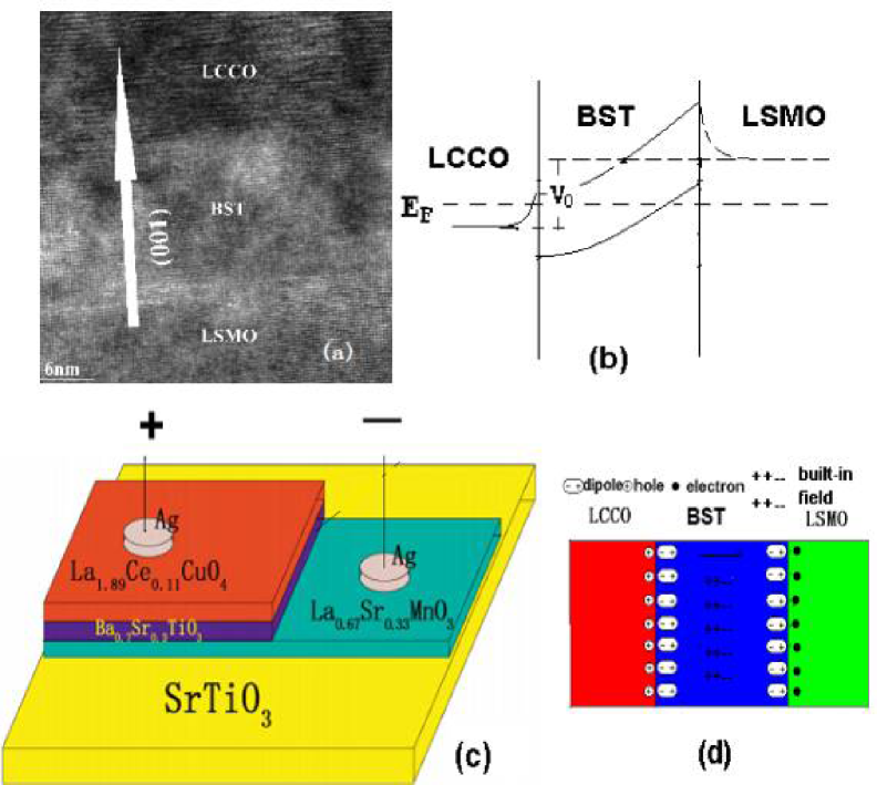
The -- junctions of LCCO/BST/LSMO are prepared by pulsed Laser deposition method on (001) SrTiO3 (STO) substrate basically following the growth conditions of LCCO, BST, and LSMOWu ; Chen ; Zhang . The thickness of each layer is controlled by the number of the pulse of the laser beam. The junctions (with both LSMO and LCCO in 100 nm) with BST with thickness 5, 15, 25, 50, and 100 nm are designed. The whole junction is in perfect epitaxial growth along (001) direction, no structure defects are observed (Fig.2(a)). The intrinsic evidence of ferroelectricity, the - hysteresis loops are observed obviously for BST20 nm in the junction (the inset of Fig. 3 (a)).
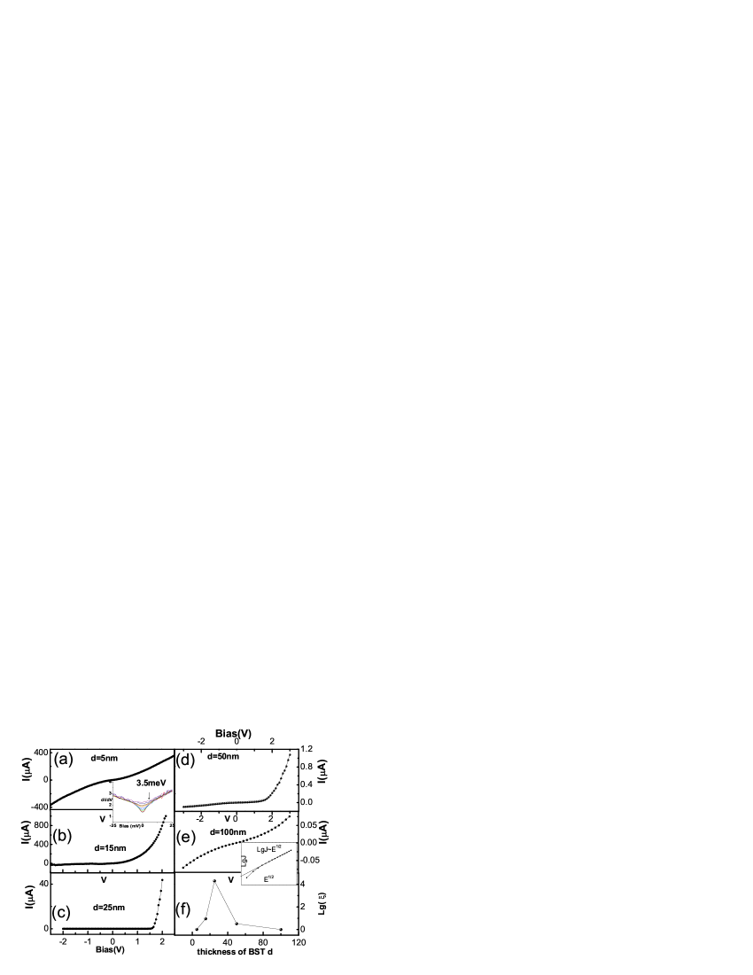
In such nanometer scale of BST, the thickness directly reflects the ferroelectricity, so the shape of - curves of the junction directly depends on the thickness of BST. Fig.1 (a-e) show the - curves of the LCCO/BST/LSMO junctions with various thickness of BST. It is clearly indicated that the ferroelectric plays the key role on the rectifying function of -- junction intrinsically based on and , the always directs from LCCO (n-region) to LSMO (p-region) in the junctionStreetman , and blocks the motion of electrons from the LCCO to LSMO. When we take the external bias voltage to be positive in LCCO relative to LSMO, the reversed polarized field of ferroelectric BST must direct from LSMO to LCCO, and suppresses the , resulting in the occurrence of the forward current from LCCO to LSMO. In the reversed bias case, the direction of of BST is the same as that of , then both and take together to largely block the reversed current. So we can conclude that the promotes the forward current, and the blocks the reversed current of the junction. As shown in Fig.2. By which, we present the high resolution TEM image of the section , the schematic of the energy band structure in the interface, and the schematic of mechanism (and design) of such metallic -- junction. The role of the ferroelectric BST is clearly presented.
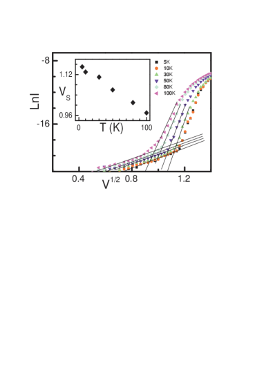
To further understand the current feature in such -- junctions, we make examination of the relation of the forward current and bias voltage for the junction with BST25nm as shown in Fig.1(c). It is shown in Fig.3 that below a bias voltage which is determined by using the , we obtained the relation of , i.e., the current obeys the Schottky modelYang , this critical bias voltage can be considered to be the Schottky barrier , which is descended with increasing temperature (the inset of Fig.3), from 1.15 V at 5 K to 0.98 V at 100 K, i.e., below , the current is limited by the Schottky emission though and exist. In the higher bias voltage, the current deviates from the Schottky model. When the bias voltage is increased till 2 V, the current seems still not to approach the Space-charge-limited model caused in heterostructure with conventional size of BSTYang , the current is completely dominated by and . So that , the BST with thickness of 2025 nm in such junction may not currently form space-charge-limited type current unless in the higher bias voltage region. The -- junction with BST20-25 nm is quite different from that with BST with thickness 50 nm, for which, as shown above the current respectively obeys the Schottky model in the low bias voltage, and Space-charge-limited model in the higher bias voltage. Therefore, based on this aspect, we may make more complete conclusion that for configuring the present -- junction, the BST layer can not be too thin since and can not form when the BST is thinner than a limitation of thickness (10 nm); the BST can not be too thick since the Schottky emission and Space-charge-limited model will dominate the current of the junction when BST is thicker than a limitation of thickness (50 nm). To form the optimal LCCO/BST/LSMO -- junctions, from the experimental data indicated above, the thickness of BST should be 20-25 nm, for which and can form and can play dominated roles in the suitable bias voltage region.
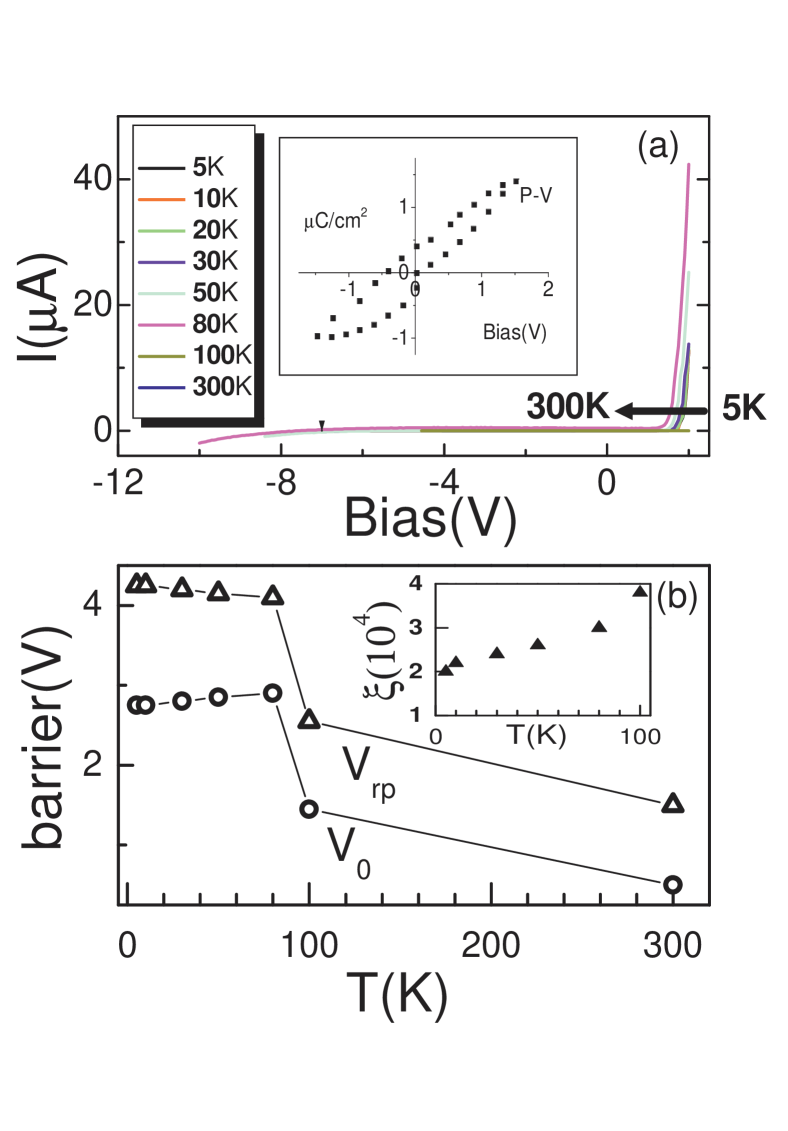
In order to reveal the ferroelectric role on the LCCO/BST/LSMO junction further, we investigated the temperature dependence of the rectifying function. Fig. 4(a) shows the temperature dependence of the - curve shape of the LCCO/BST/LSMO junction with BST 25 nm in the temperature range from 5 K to 300 K. Contrasting with the SrTiO3 switched semiconductor oxide -- junctions Sugiura_JAP_90_187 , it clearly indicates that the shape of these - curves of the present -- junctions is basically independent of the temperature. But the temperature of rectifying function is needed to be investigated carefully for the practical applications. For this kind of -- junctions, the bias voltage is of 1-2 volts, which is much larger than the superconducting energy gap, so these -- junctions all work on the normal state transport of LCCO, which doesn’t show strong temperature dependence. Therefore, the temperature dependence of the - curves of the junction should be basically caused by the temperature dependence of the ferroelectricity of BST. Intrinsically,as indicated above, switches the forward current, blocks the reversed current. So the temperature dependence of the - curve shape should originate from the temperature dependence of and . To define this, we characterize and in the following two critical points: the forward bias at which the forward current starts to occur (the criterion is A at 5 K) is the value of ; the reversed bias at which the reversed current starts to occur(the criterion is A at 5 K) is the value of sum of . Such two points can critically reveal the temperature dependence of and . At 5K, the forward current starts to occur at the forward bias voltage of 1.5V; the reversed current starts to occur at -7 V, and can be estimated by using the relation that = 1.5 V, = 7 V then = 4.25 V, = 2.75 V. By this way, every couple of and at each temperature can be defined and concluded in Fig. 4(b). On the other hand, the rectification of the junction with BST25 nm at various temperatures also can be defined. At 5K, the forward current at the forward bias of 2V is A, the reversed current at the reversed bias (-2 V) is A, the rectification, defined as =forward current at +2 V/reversed current at -2 V is . When the temperature is increased from 10 K to 80 K, the forward current at +2 V increased from 4.6 A to 7.6 A, the reversed current increase from 2 A to 2.5 A. the rectification changes from 2.3 to 3. At 100 K, the rectification has a rather larger increase, up to 3.8. At 300 K, the forward current is more than one order larger than that at 100 K (the reversed current is in A order) the rectification keeps in a high value of . So the rectification of the present -- junctions shows obvious positive temperature dependence in the temperature range up to 300 K (the inset of Fig.4(b)) and the main contributor for this is . The big change of and of the junction at 100 K may come from a phase transition of BST in the junction with such nanometer size. This should be examined further. But this big change does not make a hindrance on the rectifying function of such -- junction. Therefore, the ultrahigh rectification () and its positive temperature dependence makes the present metallic -- junction to have rich power to satisfy the requirements of the practical applications. It also indicates that the BST with wide forbidden band of 3.5 eV Dawber is a very suitable material to make oxide metallic -- junctions.
In conclusion the metallic oxide LCCO/BST/LSMO -- junctions consisting of three main kinds of functional oxides are successfully made for the first time. Due to the switch role of ferroelectric critically realized by double barrier fields and , this kind of -- junctions with BST20-25 nm show definite unique functions. Contrasting to the standard semiconductor - junctions, for which there is no forward bias for starting the forward current, and there is a finite reversed currentStreetman , the present metallic oxide -- junctions possess definite forward bias voltage for starting the forward current and possess the definite negligible reversed current, so they are the real oxide diodes with strict switch function; contrasting to the semiconductor oxide - (--) junctions for which the functions are to be defined, the present metallic oxide -- junctions possess definite ultrahigh rectifying function with positive temperature coefficient, for which the - curve shape is temperature independent. All these functions of the metallic oxide -- junctions maintain in the temperature range of 5 to 300 K, making them to be real basic devices in the field of oxide electronics.
Acknowledgements.
We thank Prof. M. Tachiki, Prof. X. Hu, Prof. X. X. Xi, for their helpful discussions. This work is supported by grants from the State Key Program for Basic Research of China (No. 2004CB619004-1) and the National Natural Science Foundation (No. 10474121).References
- (1) H. Tanaka, J. Zhang, and T. Kawai, Phys. Rev. Lett. 88, 027204 (2002).
- (2) A. Tiwari, , Appl. Phys. Lett. 83, 1773 (2003).
- (3) F. Hu , Appl. Phys. Lett. 83, 1869 (2003).
- (4) H. B. Lu , Appl. Phys. Lett. 86, 032502 (2005).
- (5) X. X. Xi, , Appl. Phys. Lett. 61, 2353 (1992).
- (6) W. Ramadan , J. Appl. Phys. 99, 043906 (2006).
- (7) M. Sugiura , J. Appl. Phys. 90, 187 (2001).
- (8) C. Mitra , Appl. Phys. Lett.79, 2408 (2001).
- (9) P. L. Lang , Appl. Phys. Lett. 87, 053502 (2005).
- (10) B. G. Streetman, Solid state electronic devices, (prentice-hall, Inc., Englewood Cliffs, New Jersy, 1980).
- (11) Y. E. Tsymbal and H. Kohlstedt, Science 313, 181 (2006).
- (12) J. Junquera and P. Ghosez, Nature (London) 422, 506 (2003).
- (13) G. Gerra, A. K. Tagantsev, N. Setter and K. Parlinski, Phys. Rev.Lett. 96, 107603(2006).
- (14) D. D. Fong , Science 304, 1650 (2004).
- (15) E. Dagotto, Rev. Mod. Phys. 66, 763 (1994).
- (16) M. Naito, and M. Hepp, Jpn. J. Appl. Phys. 39, L485-487 (2000).
- (17) L. Zhao , Supercond. Sci. Tech. 17, 1361(2004).
- (18) H. Wu , Phys. Rev. B 73, 104512 (2006).
- (19) B. Chen , Appl. Phys. Lett. 84, 583 (2004).
- (20) F. C. Zhang , Solid State Communications 131, 271 (2004).
- (21) M. B. Salamon, and M. Jaime, Rev. Mod. Phys. 73, 583 (2001).
- (22) H. Yang , Appl. Phys. Lett. 83, 1611 (2003).
- (23) M. Dawber, K. M. Rabe and J. F. Scott, Rev. Mod. Phys. 77, 1083 (2005).