Photoemission study of TiO2/VO2 interfaces
Abstract
We have measured photoemission spectra of two kinds of TiO2-capped VO2 thin films, namely, that with rutile-type TiO2 (r-TiO2/VO2) and that with amorphous TiO2 (a-TiO2/VO2) capping layers. Below the metal-insulator transition temperature of the VO2 thin films, K, metallic states were not observed for the interfaces with TiO2, in contrast with the interfaces between the band insulator SrTiO3 and the Mott insulator LaTiO3 in spite of the fact that both TiO2 and SrTiO3 are band insulators with electronic configurations and both VO2 and LaTiO3 are Mott insulators with electronic configurations. We discuss possible origins of this difference and suggest the importance of the polarity discontinuity of the interfaces. Stronger incoherent part was observed in r-TiO2/VO2 than in a-TiO2/VO2, suggesting Ti-V atomic diffusion due to the higher deposition temperature for r-TiO2/VO2.
pacs:
71.30.+h, 79.60.Dp, 73.20.-r, 73.61.-rI Introduction
Strongly correlated electron systems, especially transition-metal oxides, have been the subjects of numerous studies because of the variety of attractive behaviors including high-temperature superconductivity, giant magnetoresistance and metal-insulator transition (MIT) MIT . Among them, Ti and V oxides are typical systems in which MITs between Mott-Hubbard insulators and Fermi-liquid states have been studied MIT ; fujimori . Recently, high quality interfaces between transition-metal oxides have become available due to the development of epitaxial thin film fabrication techniques. Ohtomo et al. ohtomo have made an atomic-resolution electron-energy-loss spectroscopy study of layers of the Mott insulator LaTiO3 (LTO) embedded in the band insulator SrTiO3 (STO), and found that Ti 3 electrons are not completely confined within the LTO layer but are extended over the neighboring STO layers in spite of the chemically abrupt interfaces. Here, the Ti ion in LTO has the configuration while that in STO has the configuration, i.e., the empty band. Shibuya et al. shibuya reported the metallic behavior of the STO/LTO interfaces by measuring the electrical resistivity of STO/LTO superlattices as a function of temperature. This metallic behavior is caused by the redistribution of electrons from the LTO into STO layers up to several monolayers, making the electronic structure of the interfaces analogous to that of the metallic La1-xSrxTiO3 alloy system tokura . Okamoto and Millis okamoto ; okamoto2 have studied the spectral function of such systems by model Hartree-Fock and dynamical-mean-field-theory calculations and explained the novel metallic behavior at this interfaces between the two insulators, which they call “electronic reconstruction”. Recently, Takizawa et al. takizawa performed a photoemission spectroscopy study of LTO/STO interfaces using superlattice samples, and indeed observed metallic behavior in the interface region. In this work, we have measured photoemission spectra of another series of interfaces formed between a band insulator, TiO2, and a Mott (or Mott-Peierls) insulator, VO2, in order to see whether the metallic behavior of the STO/LTO interfaces is a universal feature of band insulator and Mott insulator interfaces or not and to gain further insight into the mechanism which causes the metallic behavior of these interfaces.
The vanadium dioxide VO2 is a well-known material which undergoes a transition between the high-temperature metallic phase and the low-temperature insulating phase morin . In the high-temperature phase, the crystal has the tetragonal rutile-type structure, while in the low-temperature phase, the V atoms dimerize and twist, distorting the crystal from the tetragonal structure to a monoclinic one. Goodenough goodenough first discussed the MIT based on a multi-band model. Abbate et al. abbate directly observed the splitting of the unoccupied band into the and components in going from the metallic phase to the insulating phase by soft x-ray absorption spectroscopy. It has been debated for many decades whether the metal-insulator transition in VO2 is derived by electron-lattice interaction (Peierls transition) or electron-electron interaction (Mott transition). The electronic structures of the metallic and insulating phase of VO2 have been discussed emphasizing electron-phonon interaction wentzcovitch , electron-electron interaction rice , and orbital degeneracy ld ; tanaka . So far several photoemission studies have been reported sawatzky ; shin ; okazaki02 ; shigemoto ; koethe on bulk VO2 single crystals. Recently, Muraoka et al. prepared VO2/TiO2 thin films which undergo an MIT near room temperature muraoka ; muraokaapl . By using thin films, it has become possible to perform detail-temperature-dependent photoemission spectroscopy (PES) studies utilizing the stability of the thin film surfaces okazaki ; eguchi . In the present work, we have studied three samples; a VO2 thin film capped with rutile-type TiO2 (r-TiO2/VO2), a VO2 thin film capped with amorphous-TiO2 (a-TiO2/VO2), and a VO2 thin film without a TiO2 capping layer. We observed no metallic states at the TiO2/VO2 interfaces region for the low-temperature phase of VO2 in contrast to the STO/LTO case takizawa .
II Experimental
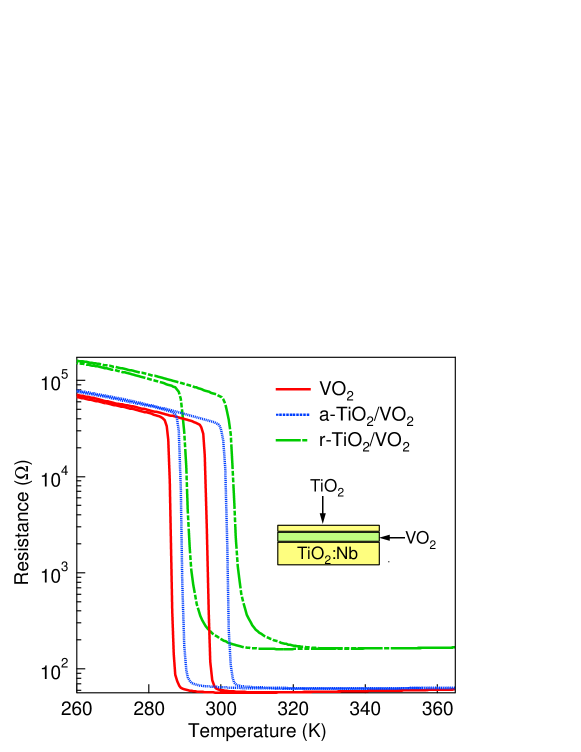
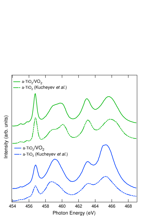
The films were prepared using the pulsed laser deposition (PLD) technique on Nb-doped TiO2(001) substrate muraoka . V2O3 pellet was used as a target to prepare VO2 thin films. During the deposition, the substrate temperature was kept at 733 K and the oxygen pressure was maintained at 1.0 Pa. The film thickness was about 10 -15 nm. The r-TiO2/VO2 sample was prepared by depositing TiO2 at 673 K on the VO2 thin film. The a-TiO2/VO2 sample was prepared by depositing TiO2 at room temperature. The thickness of the TiO2 capping layer was one to two monolayers estimated from the deposition time. Resistivity of these samples are shown in Fig. 1. MIT was clearly observed in all the samples. The atomic structures of the TiO2 capping layer were confirmed by comparing the Ti 2 x-ray absorption spectra with the previous results reported by Kucheyev Ti2pXAS as shown in Fig. 2. Due to the different TiO2 deposition temperatures between r-TiO2/VO2 and a-TiO2/VO2, Ti and V atoms at the r-TiO2/VO2 interface may be more strongly interdiffused than those at the a-TiO2/VO2 interface as we shall see below.
PES measurements in the soft x-ray region were performed at BL-2C of Photon Factory, High Energy Accelerators Research Organization (KEK). The measurements were performed under an ultrahigh vacuum of Torr from room temperature down to 150 K, using a Scienta SES-100 electron-energy analyzer. The total energy resolution was set to about 200 meV. Resonant photoemission spectroscopy (RPES) measurements at the V 2 3 absorption edge were performed to eliminate contributions from the TiO2 capping layers. The Fermi-level () position was determined by measuring gold spectra. X-ray absorption spectroscopy (XAS) was performed in the total-electron-yield mode. The samples were transferred from the PLD chamber to the spectrometers through the air, and no surface treatment was made. During the measurements, the samples were kept at room temperature (RT) to study the metallic phase, or at 220 - 250 K to study the insulating phase.
III Results and discussion
Figure 3 shows the RPES spectra of a-TiO2/VO2 for different photon energies. The V 3 band was most strongly enhanced at 518 eV, due to V 2 3 resonance.
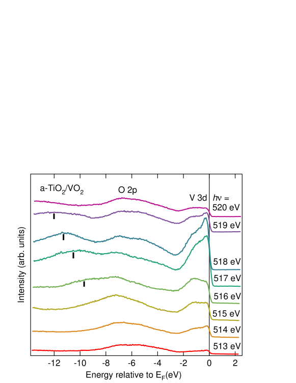
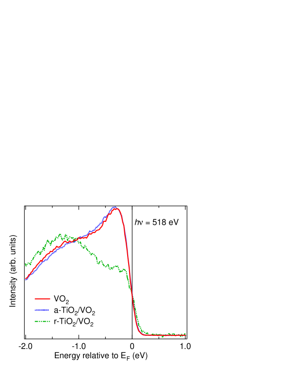
Figure 4 shows the RPES spectra of the VO2, a-TiO2/VO2, and r-TiO2/VO2 samples in the V 3 band region measured at room temperature, i.e, spectra in which VO2 was metallic. Each spectrum consisted of the coherent part (from -0.5 eV to ) and the incoherent part (from -2.0 eV to -0.5 eV). The spectra have been normalized to the integrated area in the V 3 band region. The spectrum of a-TiO2/VO2 was nearly identical to those of the VO2 film. On the other hand, those of r-TiO2/VO2 had stronger incoherent part than those of a-TiO2/VO2. Perhaps the amorphous TiO2 layer did not form chemical bonding with the VO2 surface and did not affect the electronic structure of the VO2 film in the interface region.
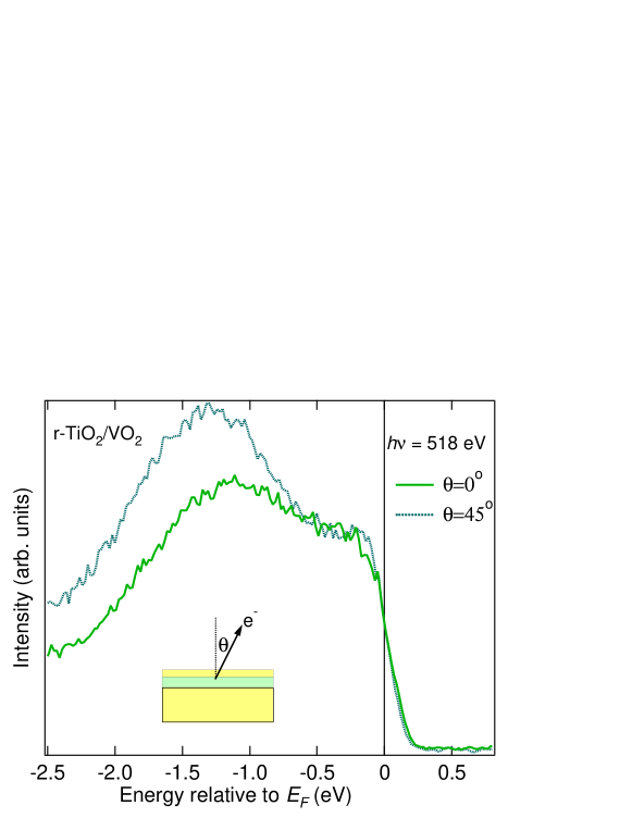
In order to see the origin of the strong incoherent part for r-TiO2/VO2, the sensitivity of the photoemission measurements to the interface was varied by changing the emission angle as shown in Fig. 5. One can see that the incoherent part was enhanced as emission angle was increased, which indicates that the stronger incoherent part came from the interface region of r-TiO2/VO2. The different spectral weight distributions of the coherent and incoherent parts between r-TiO2/VO2 and a-TiO2/VO2 may have been caused by the different temperatures during the TiO2-capping process. In the r-TiO2/VO2 sample, for which the TiO2-capping layer was deposited at a higher temperature, Ti and V atoms may be interdiffused to some extent, and the interface region may become somewhat like V1-xTixO2, which becomes less conducting as the Ti concentration increases Tidope .
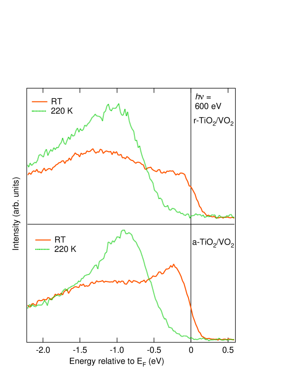
The temperature dependence of the V 3 valence-band spectra for r-TiO2/VO2 and a-TiO2/VO2 is shown in Fig. 6. In both samples, a metallic signature, namely, the Fermi edge was not observed below the MIT temperature of the samples (Fig. 6) at the interface between the insulating TiO2 and the insulating phase of VO2, in contrast with the case of the STO/LTO interface takizawa , although TiO2 and VO2 have and configurations, respectively, like STO and LTO.
Since the metallic behavior of the STO/LTO interfaces comes from the extended distribution of electrons from the LTO to STO layers, the present result indicates that the electrons in VO2 are confined within the VO2 layer and are not redistributed into the TiO2 capping layer. One possible explanation for the confinement of electrons can be made from the view point of atoms constituting the interface: While TiO2/VO2 is composed of different transition-metal atoms, Ti and V, STO/LTO is composed of the same transition-metal atom, Ti. Therefore, the stronger attractive potential of the V atomic core than that of Ti may prevent electrons at the V site from being redistributed into the TiO2 layer. From the crystal structure point of view, on the other hand, TiO2/VO2 has the rutile structure in which the d-band width is narrower than that of the perovskite structure and electrons may be more easily confined across the interface. The dielectric constant of the capping layer may also be important through the screening of electric potential: STO has a much larger dielectric constant than TiO2 vonHippel , and may weaken the attractive potential of the Mott insulating layer compared to TiO2. Moreover, the fact that VO2 is not a simple Mott insulator but is a “Mott-Peierls insulator”, where the Mott transition is accompanied by a crystal distortion, may also be important. Apart from the above various possibilities, we point out the fact that the penetration of electrons from the LTO to STO layers can be triggered by the polarity discontinuity at the interface: In order to avoid the macroscopic electric field generated across the polar LTO layer (TiO2-/LaO+/TiO2-/…), that is, in order to avoid the so-called “polarity catastrophe” nakagawa ; hotta , part of the electronic charges should be transferred from the negatively charged TiO2-layer side to the positively charged LaO-layer side of the LTO layer, causing the fractional occupation of the d band in both interface regions, and hence the metallic state. In the case of the TiO2/VO2 interfaces, since the valence of V in VO2 and that of Ti in TiO2 are the same, such polarity discontinuity would not occur at the interface and the fractional occupancy of the d band would not occur. To confirm this scenario, systematic comparative studies of polarity discontinuous and continuous interfaces are necessary.
IV Summary
We have performed photoemission measurements on TiO2-capped VO2 thin films. All the 3d band spectra showed the coherent and incoherent parts and the coherent part disappeared in the insulating phase of VO2. While a-TiO2/VO2 showed spectra almost identical to uncapped VO2 thin film, the incoherent part was enhanced in r-TiO2/VO2, which we attribute to the interdiffusion of Ti and V atoms across the interfaces. Metallic state was not observed in the interfaces between the band insulator TiO2 and the Mott-Peierls insulator VO2 at low temperature for all the samples in contrast to the STO/LTO interfaces. We suggest that this is originated from the absence of polarity discontinuity at the TiO2/VO2 interface unlike the case of STO/LTO.
Acknowledgments
This work was supported by a Giant-in-Aid for Scientific Research (A16204024) from JSPS and that for Priority Area “Invention of Anomalous Quantum Materials” (16076208) from the Ministry of Education, Culture, Sports, Science and Technology of Japan. The work at KEK-PF was done under the approval of Photon Factory Program Advisory Committee (Proposal No. 2005G101).
References
- (1) M. Imada, A. Fujimori, and Y. Tokura, Rev. Mod. Phys. 70, 1039 (1998).
- (2) A. Fujimori, I. Hase, H. Namatame, Y. Fujishima, Y. Tokura, H. Eisaki, S. Uchida, K. Takegahara, and F. M. F. de Groot, Phys. Rev. Lett. 69, 1796 (1993).
- (3) A. Ohtomo, D. A. Muller, J. L. Grazul, and H. Y. Hwang, Nature 419, 328 (2002).
- (4) K. Shibuya, T. Ohnishi, M. Kawasaki, H. Koinuma, and M. Lippmaa, Jpn. J. Appl. Phys. 43, L1178 (2004).
- (5) Y. Tokura, Y. Taguchi, Y. Okada, Y. Fujishima, T. Arima, K. Kumagai, and Y. Iye, Phys. Rev. Lett. 70, 2126 (1993).
- (6) S. Okamoto and A. J. Millis, Nature 428, 630 (2004).
- (7) S. Okamoto and A. J. Millis, Phys. Rev. B 70, 241104(R) (2004).
- (8) M. Takizawa, H. Wadati, K. Tanaka, M. Hashimoto, T. Yoshida, A. Fujimori, A. Chikamatsu, H. Kumigashira, M. Oshima, K. Shibuya, T. Mihara, T. Ohnishi, M. Lippmaa, M. Kawasaki, H. Koinuma, and S. Okamoto, and A. J. Millis, Phys. Rev. Lett. 97, 057601 (2006).
- (9) F. J. Morin, Phys. Rev. Lett. 3, 34 (1959).
- (10) J. Goodenough, Phys. Rev. 117, 1442 (1971).
- (11) M. Abbate, F. M. F. de Groot, J. C. Fuggle, Y. J. Ma, C. T. Chen, F.Sette, A. Fujimori, Y. Ueda, and K. Kosuge, Phys. Rev. B 43, 7263 (1991).
- (12) R. M. Wentzcovitch, W. W. Schulz, and P. B. Allen, Phys. Rev. Lett. 72, 3389 (1994).
- (13) T. M. Rice, H. Launois, and J. P. Pouget, Phys. Rev. Lett. 73, 3042 (1994).
- (14) M. W. Haverkort, Z. Hu, A. Tanaka, W. Reichelt, S. V. Streltsov, M. A. Korotin, V. I. Anisimov, H. H. Hsieh, H.-J. Lin, C. T. Chen, D. I. Khomskii, and L. H. Tjeng, Phys. Rev. Lett. 95, 196404 (2005).
- (15) A. Tanaka, J. Phys. Soc. Jpn. 73, 152 (2004).
- (16) S. Shin, S. Suga, M. Taniguchi, M. Fujisawa, H. Kanzaki, A. Fujimori, H. Daimon, Y. Ueda, K. Kosuge, and S. Kachi, Phys. Rev. B 41, 4993 (1990).
- (17) K. Okazaki, A. Fujimori, and M. Onoda, J. Phys. Soc. Jpn. 71, 822 (2002).
- (18) A. Shigemoto, S. Suga, A. Sekiyama, S. Imada, A. Yamasaki, A. Irizawa, S. Kasai, T. Muro, Y. Saitoh, Y. Ueda, and K. Yoshimura, J. Electron Spectrosc. Relat. Phenom. 144-147, 837 (2005).
- (19) T. C. Koethe, Z. Hu, M. W. Haverkort, C. Schüßler-Langeheine, F. Venturini, N. B. Brookes, O. Tjernberg, W. Reichelt, H. H. Hsieh, H. J. Lin, C. T. Chen, and L. H. Tjeng, Phys. Rev. Lett. 97, 116402 (2006).
- (20) G. A. Sawatzky and D. Post, Phys. Rev. B 20, 1546 (1979).
- (21) Y. Muraoka, Y. Ueda, and Z. Hiroi, J. Phys. Chem. Solids 63, 965 (2002).
- (22) Y. Muraoka and Z. Hiroi, Appl. Phys. Lett. 80, 583 (2002).
- (23) K. Okazaki, H. Wadati, A. Fujimori, M. Onoda, Y. Muraoka, and Z. Hiroi, Phys. Rev. B 69, 165104 (2004).
- (24) R. Eguchi, S. Shin, A. Fukushima, T. Kiss, T. Shimojima, Y. Muraoka, and Z. Hiroi, Appl. Phys. Lett. 87, 201912 (2005).
- (25) S. O. Kucheyev, T. van Buuren, T. F. Baumann, J. H. Satcher, T. M. Willey, R. W. Meulenberg, T. E. Felter, J. F. Poco, S. A. Gammon, and L. J. Terminello, Phys. Rev. B 69, 245102 (2004).
- (26) F. Beteille, R. Morineau, and J. Livage, Materials Research Bulletin 32, 1109 (1997).
- (27) R. von Hippel, Dielectric materials and applications (The Technology Press of MIT and John Wiley & Sons, 1954).
- (28) N. Nakagawa, H. Y. Hwang, and D. A. Müller, Nature Materials 5, 204 (2006).
- (29) Y. Hotta, H. Wadati, A. fujimori, T. Susaki, and H. Y. Hwang, cond-mat/0607547.