Also at ]Nano Devices Research center, Korea Institute of Science and Technology
Also at ]Nano Devices Research center, Korea Institute of Science and Technology
Local Hall effect in hybrid ferromagnetic/semiconductor devices
Abstract
We have investigated the magnetoresistance of ferromagnet-semiconductor devices in an InAs two-dimensional electron gas system in which the magnetic field has a sinusoidal profile. The magnetoresistance of our device is large. The longitudinal resistance has an additional contribution which is odd in applied magnetic field. It becomes even negative at low temperature where the transport is ballistic. Based on the numerical analysis, we confirmed that our data can be explained in terms of the local Hall effect due to the profile of negative and positive field regions. This device may be useful for future spintronic applications.
pacs:
85.30.F, 74.25.F , 85.70Recently, two-dimensional electron gas (2DEG) systems combined with micromagnets have attracted much attention not only for fundamental physics,R1 but also for device applications.R0 ; R2 ; R3 ; R5 ; SJ In hybrid ferromagnet-semiconductor devices, inhomogeneous magnetic field is generated by micromagnets on top of 2DEG and acts as the magnetic barrier to moving charge carriers. The complex charge build-up in the Hall bar leads to interesting phenomena in longitudinal as well as transverse resistance. This local Hall effect can be used as spintronic devices,R0 magnetic field sensors,R2 non-volatile memory cells,R3 and micromagnetometers.R5 In this paper, we present the hybrid ferromagnet-semiconductor devices in which the longitudinal resistance is a mixture of even and odd contributions in external magnetic field, but the transverse resistance is odd. This interesting feature of our device can be understood in terms of local Hall effect caused by a sinusoidal magnetic field profile.
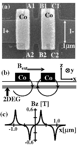
Our device structure is displayed in Fig. 1(a) as a scanning electron microscope image. An InAs 2DEG mesa, with a current channel (from to ) and six voltage probes (denoted as A1, B1, C1, A2, B2, and C2), was patterned by e-beam lithography. The current channel is 1 m wide and the voltage probes are separated about 0.6 m from center to center. Two 300 nm thick micromagnets were deposited on top of the InAs 2DEG mesa by e-beam evaporation of Co. The InAs 2DEG resides 35.5 nm below the surface. Fig. 1(b) is a schematic cross sectional view of the sample and the profile of the fringe field generated near the edges of the micromagnets. The - plane is defined by the 2DEG mesa with the -axis along the current direction ( to ). External magnetic field () aligns the magnetization () of micromagnets along the -axis and the micromagnets generate the fringe field component () normal to the 2DEG plane. Calculated is plotted in Fig. 1(c) as a function of when micromagnets are fully magnetized along the direction. is sinusoidal with two maxima and two minima and is proportional to . The centers of the voltage probes are positioned close to the maximum or minimum . The mobility and the carrier density of the devices are 7.9 m2/Vsec and m-2, respectively, at 2 K and 2.0 m2/Vsec and m-2 at 300 K. Resistance was measured using a standard lock-in technique with low-frequency (98 Hz) ac current of 1 A.
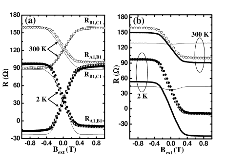
In Fig. 2(a), longitudinal resistances (between A1 and B1) and are plotted as a function of external magnetic field at 2 K and 300 K. Two curves of and are almost symmetric each other with respect to the resistance axis. () was also measured and was nearly the same as (). , defined by the difference between the maximum and the minimum longitudinal resistance, is relatively large. is 60 at 300 K and 107 at 2 K for . The sensitivity of longitudinal resistance to is estimated with at zero field, whose value is /T at 300 K and 178 /T at 2 K. In a uniform magnetic field normal to the 2DEG system, the longitudinal resistance (magnetoresistance) is an even function of the external magnetic field while the transverse (Hall) resistance is an odd function. However, the longitudinal resistance in our device has both even (magnetoresistance) and odd (Hall) contributions as displayed in Fig. 2(b), and becomes even negative in high field at 2 K. This interesting feature in our longitudinal resistance in fact arises from local Hall effect due to a sinusoidal variation of local magnetic field, as we shall explain below.
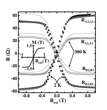
Fig. 3 shows the transverse resistance, and . (not shown) is almost the same as . Taking into account a possible minor misalignment of Hall voltage probes, we may conclude that the transverse resistance is an odd function of external magnetic field, as in a uniform magnetic field. The approximate relation, , means that near A1 and A2 is directed opposite to near B1 and B2, but the field strength is almost equal at both regions. Our data clearly support the sinusoidal variation of local magnetic field on the 2DEG system.
In order to elucidate the origin of our interesting experimental data, we calculated the resistance numerically in the diffusive as well as ballistic transport regimes. The diffusive transport model R7 is adopted at 300 K (the mean free path of electrons, m at 300 K, is shorter than the device size.) The electrostatic potential and the current density were obtained by solving the continuity equation R7 with the spatial dependent conductivity tensor (inhomogeneous magnetic field). We adopted the ballistic Landauer-Bttiker formalism LB1 at 2 K (m is longer than the device size.) Transmission probability was computed particle1 ; particle2 by injecting electrons with Fermi velocity from one lead and by counting the number of electrons exiting the other lead. In the meantime, injected electrons are subject to Newton’s equation of motion particle1 ; particle2 under the magnetic barriers.
In our numerical simulations, we took into account the device geometry including the shape of the voltage probes. The profile of local magnetic field () [see Fig. 1(c)] is obtained from dipole field dpfield of micromagnet magnetization . After computing the resistance as a function of , we tried to fit the experimental transverse resistance with theoretical one (solid lines in Fig. 3), by adjusting the (theory) versus (experiment) curve. The resulting functional form at 2 K (not shown for 300 K) is shown in the inset of Fig. 3 and is similar to the Brillouin function as expected. Other solid lines in Fig. 2(a) and Fig. 3 are theoretical resistance curves with adjusted . To conclude, we were able to reproduce the main features of our resistance curves in terms of local Hall effect due to a sinusoidal magnetic field [Fig. 1(c)].
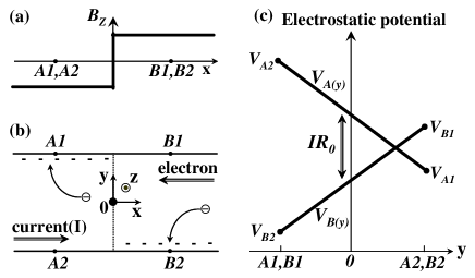
In order to better understand the transport process in the Hall bar, we consider an inhomogeneous field distribution of Fig. 4. This field profile of a step function mimics the profile of in our device [see Fig. 1(c)] from A1 (negative minimum) to B1 (positive maximum). The schematic of the current channel is displayed in the - plane in Fig. 4(b). Moving electrons are deflected by the Lorentz force under magnetic field () and piled up on the side of the device. Because is positive (negative) at the right (left) side, electrons are piled up on the B2 (A1) side as displayed. This local Hall effect explains our resistance data as we shall show below.
The accumulation of negative charges lowers the electrostatic potential at A1 (B2) with respect to A2 (B1). The resulting electrostatic potentials are displayed in Fig. 4(c). [] is the potential along the straight line from A2 to A1 [B2 to B1] in the sample. When is zero, we have = and =, and and will be simply constant functions. In this case, the voltage difference between two curves can be expressed as from Ohm’s law [], where is the current and is the longitudinal resistance in the absence of magnetic field. As magnetic field is introduced, charge piling-up gives rise to and in Fig. 4(c). Due to the symmetry of charge distribution in Fig. 4(b), the voltage difference at [] in Fig. 4(c) remains as , which is denoted by an arrow. Further the Hall voltages and have the same magnitude with an opposite sign, thanks to the symmetry in Fig. 4. Combining the above results, we can express as
| (1) |
where is the transverse (Hall) resistance between probes A2 and A1. This relation explains why the longitudinal resistance curve has a term odd in . Though Eq. (1) is derived from a simple field profile, it is quite amusing to note that is comparable to antisymmetric part of in Fig. 2(b) when is considered as symmetric part.
When electrons are piled up at A1 with respect to B1 sufficiently or is sufficiently strong in the right direction, locally induced Hall field between A1 and B1 can overcome applied current-driven electric field. This local inversion of the electric potential profile leads to the observed negative longitudinal resistance (NLR). We can also explain the NLR in terms of Eq. (1). The mobility increases with lowering temperature, which results in decrease of and increase of (see Fig. 3.) If is strong enough for to be larger than , the NLR occurs.
In summary, we fabricated ferromagnet-semiconductor hybrid devices in which the dipolar field of micromagnets is of a sinusoidal form on the Hall bar. The longitudinal resistance is featured with mixing of even and odd terms in external magnetic field (), while the transverse (Hall) resistance is odd. Due to odd term in , our longitudinal resistance becomes even negative in high field at low temperature. Based on numerical calculations in the diffusive and ballistic transport regimes, we confirmed that our interesting data can be explained in terms of the combined local Hall effect in the positive and negative magnetic field regions. We suggested a simple model which can explain the main results of our experiments. Our result demonstrates that the control of local magnetic field by micromagnets can provide another degree of freedom for device applications.
This work was supported by the Vison21 Program at Korea Institute of Science and Technology, the SRC/ERC program of MOST/KOSEF (R11-2000-071), and the Basic Research Program of KOSEF (R01-2006-000-11391-0).
References
- (1) J. Hong, V. Kubrak, K. W. Edmond, A. C. Neumann, B. L. Gallagher, P. C. Main, M. Henini, C. H. Marrows, B. J. Hickey, and S. Thoms, Physica E 12, 229 (2002).
- (2) J. Wrobel, T. Dietl, A. Lusakowski, G. Grabecki, K. Fronc, R. Hey, K. H. Ploog, and H. Shtrikman, Phys. Rev. Lett. 93, 246601 (2004)
- (3) N. Overend, A. Nogaret, B. L. Gallagher, P. C. Main, M. Henini, C. H. Marrows, M. A. Howson, and S. P. Beaumont, Appl. Phys. Lett. 72, 1724 (1998).
- (4) M. Johnson, B. R. Bennett, M. J. Yang, M. M. Miller, and B. V. Shanabrook, Appl. Phys. Lett. 71, 974 (1997).
- (5) M. Governale and D. Boese, Appl. Phys. Lett. 77, 3215 (2000).
- (6) S. Joo, J. Hong, K. Rhie, K. Y. Jung, K. H. Kim, S. U. Kim, B. C. Lee, W. H. Park, and K.-H. Shin, J. Korean Phys. Soc. 48, 642 (2006).
- (7) I. S. Ibrahim, V. A. Schweigert, and F. M. Peeters, Phys. Rev. B 56, 7508 (1997).
- (8) M. Bttiker, IBM J. Res. Dev. 32, 317 (1988); C. W. J. Beenakker and H. van Houten, Phys. Rev. Lett. 63, 1857 (1989).
- (9) B. J. Baelus and F. M. Peeters, Appl. Phys. Lett. 74, 1600 (1999).
- (10) F. M. Peeters and X. Q. Li, Appl. Phys. Lett. 72, 572 (1998).
- (11) T. Vancura, T. Ihn, S. Broderick, and K. Ensslin, W. Wegscheider, and M. Bichler, Phys. Rev. B 62, 5074 (2000).