Ideal switching effect in periodic spin-orbit coupling structures
Abstract
An ideal switching effect is discovered in a semiconductor nanowire with a
spatially-periodic Rashba structure. Bistable ‘ON’ and ‘OFF’ states can be
realized by tuning the gate voltage applied on the Rashba regions. The
energy range and position of ‘OFF’ states can be manipulated effectively by
varying the strength of the spin-orbit coupling (SOC) and the unit length of
the periodic structure, respectively. The switching effect of the nanowire
is found to be tolerant of small random fluctuations of SOC strength in the
periodic structure. This ideal switching effect might be applicable in
future spintronic devices.
PACS Numbers: 71.70.Ej, 85.35.Be
Spin freedom of electrons in semiconductors can be manipulated efficiently through the mechanism of spin-orbit couplings (SOCs) Lutt ; Dres ; Rash , which has been confirmed in experiments Wund . Among the several types of SOCs in semiconductors, Rashba SOC Rash , which results from asymmetric electric confinement in nanostructures, is the most attractive one, due to its strength tuned easily by external gate voltage Nitt ; Enge . Various spintronic devices, such as the spin filter Koga , spin valve Mats , and spin-field-effect transistor Datt have been brought forward in two dimensional electron gases with Rashba interactions. Since no external magnetic field is required to realize the control of spin of electrons, all-electrical fabrication of practical devices has been expected in such kinds of systems Popescu ; Step .
Very recently, based on Rashba and/or Dresselhaus SOCs, Jiang et al. Jiang and Gong et al. Yang discovered an interesting switching effect of electronic flow in a one-dimensional electron gas sandwiched between two electrodes. The transmission coefficient of electrons in the drain electrode can be varied from 1 to 0 by tuning the SOC strength. However, in both schemes, the behavior of the switching effect is strongly dependent on the height of the scattering potentials at the interfaces between sample and electrodes. With a high interfacial barrier, ‘ON’ state of the switch can not work effectively: the total transmission peak is too sharp to gain a stable ‘ON’ state. While with a relatively low barrier, ‘OFF’ state can not be absolutely reached: there is usually considerable leakage in the ‘OFF’ state even if the SOC strength is tuned to the maximum value permitted in current experiments Nitt ; Enge . And the barrier height, to our knowledge, can not be controlled effectively by experimental tacts. All these reduces the feasibility of the practical application of their switching schemes.
In the present work, an ideal switching effect is found in a one-dimensional semiconductor quantum wire with spatially-periodic Rashba structure, where SOC and non-SOC segments connect in series alternately. The principle of the effect can be rationalized by the transport properties of the electrons in the wire. When an appropriate magnitude of Rashba strength is provided, an energy gap can be formed near the boundaries of Brillouin zone due to the periodic Rashba potential. This causes the incident electrons with energies in the gap reflected totally. If Rashba strength is tuned to be smaller than a critical value, all the incident electrons can be transmitted. Therefore, stable ‘rectangle-type’ switching effect can be obtained by controlling the Rashba SOC. Our further investigation shows that the ideal switching behavior survives from small fluctuations of the Rashba strengths in the periodic structure.
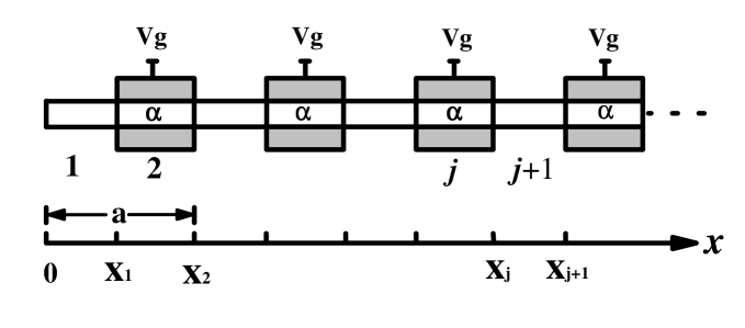
The geometry we consider is a one-dimensional quantum wire Note with periodic Rashba structure illustrated in Fig.1. Each periodic unit consists of one non-SOC segment and one SOC segment with the same length of ( is set at 24 nm in the following calculations except the case in Fig. 2 (b)). The symbol of in the figure expresses the applied gate voltage to control the Rashba strength. Note that in our model the SOC and non-SOC segments are composed of the same semiconductor material. Therefore, if gate voltage is removed (i.e. Rashba SOC is neglected), all the segments unite into a homogeneous structure. In the calculation, an electron wave is injected from the left to the right along direction.
The Hamiltonian in SOC segment can be written as:
| (1) |
where the effective mass of electrons is set as 0.067 is the mass of the free electron), is the vector of the Pauli matrix, and is the -component of the momentum operator. The parameter describes the SOC strength. To determine the final transmission coefficient after propagating through the whole quantum wire, we need consider the transmission process of an electron with energy through one unit, and obtain the transfer matrix. To provide a clear illustration, we lable the segments in series: , as shown in Fig.1. The even stands for SOC segments, and the wave function in it can be expressed as: , where, . The denotions and express the eigenspinor states and , respectively. Similarly, odd stands for the non-SOC segments, where the wave function can be written in the same form as SOC segment with, however, different wave vectors: ().
Using boundary conditions at the interfaces of non-SOC/SOC, i.e. the continuous conditions of wave functions and conservation ones of the current Mats ; Zuli ; Sun , we can get the following transfer matrix for the wave functions at and segments.
| (2) |
where
Note that and are related with the coordinates, while and are not. The transfer matrix for the wave function in the th segment can be deduced as: , from which the coefficients in the th segment can be expressed as:
| (3) |
From Eq. (3), the transmitted wave function in the th segment can be obtained if the incident wave function is known. The total transmission coefficient () of spin up and down states in the th segment is then calculated. In the switch scheme, ‘’ and ‘’ correspond to ideal ‘ON’ and ‘OFF’ states of the outgoing wave, respectively.
In order to understand the switching effect well, we calculate the band structure of the periodic structure by using the plane wave method. The wave function can be expressed as: , where and are expanded in plane waves: , where is the total length of the nanowire, is the reciprocal lattice vector, . The Rashba interaction is modulated periodically along direction (see Fig.1), and expanded as Solving the schrödinger equation in reciprocal space, we get two coupling equations:
| (4) |
| (5) |
For each , there are two equations like above. If the total number of plane waves used is , there will be coupling equations, corresponding to coefficients , . The eigenvalues at each point can be solved by diagonalizing the secular equation.
The transmission coefficient as a function of the incident energy of electrons at different Rashba strengths are shown in Fig.2(a). The striking feature in the figure is the appearance of energy gaps, within which the transmission coefficient . When Rashba strength a.u. ( a.u. eVm), the width of the gap is about meV (roughly from 9.1 to 9.6 meV). That means the incident electrons with the energies in this range will be reflected totally by the periodic structure. The width of the gap is found to be sensitively dependent on the Rashba strength. It is clear that the gap becomes larger with the increase of the Rashba strength. In addition, the gap is also related with the number of the repeated periodic units in the structure (the repeated number is set at in the calculation for the periodic structure). At the same Rashba strength, the gap width will increase with the increase of the number of the periodic units till it reaches a saturated value. A larger number of units and a stronger are expected to produce a wider gap. In the practical case, appropriate value and number of units may be chosen.

To realize the switching effect, we hope that the Fermi energy of the incident electrons is located within the energy gap, so that electrons can not transmit through the quantum wire. This state then corresponds to ‘OFF’ state of a switch. In Fig.2(b), we fix the SOC strength a.u., and pay our attention to the gap position under different lengths of unit cell. It can be seen that the gap shifts toward lower energy region with the increase of , which can be rationalized by the property of band structure (in the following). Therefore, by selecting appropriate lengths of , the position of the energy gap can be modulated according to the position of the Fermi energy.
From Fig.2(a), we also find that only when the incident energy of the electrons is within the energy gap, Rashba SOC has the decisive contribution to the transmission coefficient. Beyond the gap, the contribution of the Rashba SOC is negligible (). The oscillations of transmission varying from to as the energy approaches to the position of the energy gap can be ascribed to the abrupt transition from SOC/non-SOC interface Reyn . To clearly illustrate the contribution of the Rashba SOC, we plot the dependence of transmission coefficient on the Rashba strength in Fig.3, in which the incident energies are given as and meV. All of the energies are located in the transmission gap shown by the case of solid curve in Fig.2(a). Obviously, we obtain a binary “rectangle-type” transmission behavior with values of and by tuning the Rashba strength continuously. For a given energy (for example, meV), we can find a critical value ( corresponds to the peak in the solid curve). When , a nearly total transmission is achieved, corresponding to ‘ON’ state. When no electron can be transmitted, corresponding to ‘OFF’ state. It is found that small incident energy corresponds to large , which can be illustrated by the trends of as a function of at different Rashba strengths shown in Fig.2(a). In reality, the incident energies of the electrons may range from to (suppose we need to find (corresponding to and corresponding to When the switch is ‘OFF’, when the switch is ‘ON’.

To gain a deep insight into the properties of the spintronic switch, we investigate the band structure of the one-dimensional system with periodic Rashba potential. Figure 4(a) shows the band structures without () and with Rashba SOC ( a.u.), respectively. Comparing the solid curve and the dotted one, we find that due to the Rashba spin-orbit interaction, the degenerate band structure splits into two subbands: one is for spin-up and the other for spin-down. Here we emphasize the energy gap near the boundaries of Brillouin Zone. With the same parameters as in the case of solid curve in Fig.2(a), the gap width in Fig.4(a) is also about 0.5 meV from 9.1 to 9.6 meV. There is, in fact, difference in the geometries between Fig.4(a) and Fig.2(a). For the band structure calculation, the one-dimensional system is infinitely long, while the spintronic switch is a quantum wire with finite length. The fact that Fig.4(a) and Fig.2(a) produce almost the same gap demonstrates that the length of the periodic Rashba structure in Fig.2(a) is long enough to be equivalent to the infinite one. With weak Rashba strength, the difference from the two structures can be observed. In Fig.2(a), when Rashba strength is decreased to 0.02 a.u., the energy gap is smeared out. If we increase the number of the periodic unit cell, the gap will be opened.

In a practical case, we usually can not get a perfect periodic structure, for example, may fluctuate from its set value. Here we consider a disordered SOC structure, i.e. the Rashba strengths in SOC segments are randomly given, and investigate its switching effect. Figure 4(b) is the case that Rashba strengths randomly fluctuate from 0.02 a.u. to 0.03 a.u.. Compared Fig.4(b) with the dashed curve of Fig.2(a), whose Rashba strength is set at 0.025 a.u. (the average value of 0.02 a.u. and 0.03 a.u.), it is found that the energy gaps in the two cases show little difference. Therefore, it can be inferred that the switch effect we obtained is tolerant of such disorder. In additional, to our knowledge, in a one-dimensional system, the presence of disorder will induce localized states of electrons, which is a critical difference between periodic and disordered systems. Therefore, the ‘OFF’ state may be achieved due to the localized states in an ideal disordered system. For example, if the number of periodic units in the structure increases from 100 in Fig.4(b) to 1000 in Fig.4(c), the small dips in the energy region of 2.0 to 8.0 meV will become deeper. Some gaps may form with the further increase of the length of the structure.
Conclusion: A perfect switching effect of electronic flow is found in a one-dimensiaonl nanowire with spatially-periodic Rashba spin-orbit coupling. Stable ‘rectangle-type’ switching effect is obtained by controlling the Rashba SOC strength. The switch effect behaves fairly well even if the fluctuations of Rashba strengths destroy the periodic structure to some extent.
The authors are grateful to Prof. R. B. Tao at Fudan University for very helpful discussion. This work was supported by the National Natural Science Foundation of China with grant Nos.10304002 and 1067027, the Grand Foundation of Shanghai Science and Technology (05DJ14003), PCSIRT.
References
- (1) E-mail address: zyang@fudan.edu.cn.
- (2) J. M. Luttinger, Phys. Rev. 102, 1030 (1956).
- (3) G. Dresselhaus, Phys. Rev. 100, 580 (1955).
- (4) Y. A. Bychkov and E. I. Rashba, J. Phys. C 17, 6039 (1984).
- (5) N. P. Stern, S. Ghosh, G. Xiang, M. Zhu, N. Samarth, and D. D. Awschalom, Phys. Rev. Lett. 97, 126603 (2006); J. Wunderlich, B. Kaestner, J. Sinova, and T. Jungwirth, Phys. Rev. Lett. 94, 047204 (2005); Y. K. Kato, R. C. Myers, A. C. Gossard, and D. D. Awschalom, Science 306, 1910 (2004).
- (6) J. Nitta, T. Akazaki, H. Takayanagi, and T. Enoki, Phys. Rev. Lett. 78, 1335 (1997).
- (7) G. Engels, J. Lange, Th. Schäpers, and H. Lüth, Phys. Rev. B 55, R1958 (1997).
- (8) T. Kago, J. Nitta, H. Takayanagi, and S. Datta, Phys. Rev. Lett. 88, 126601 (2002).
- (9) T. Matsuyama, C.-M. Hu, D. Grundler, G. Meier, and U. Merkt. Phys. Rev. B, 65, 155322 (2002).
- (10) S. Datta and B. Das, Appl. Phys. Lett. 56, 665 (1990).
- (11) A. E. Popescu and R. Ionicioiu, Phys. Rev. B 69, 245422 (2004).
- (12) D. Stepanenko and N. E. Bonesteel, Phys. Rev. Lett. 93, 140501 (2004).
- (13) K. M. Jiang, Z. M. Zheng, B. G. Wang, and D. Y. Xing, Appl. Phys. Lett. 89, 012105 (2006).
- (14) S.J. Gong and Z.Q. Yang, cond-mat/0604346.
- (15) For example, the model can describe well a quasi-1DEG system with width less than 20 nm, since the first confinement energy of the geometry is found to be higer than 20 meV and the Fermi energy of a semiconductor 2DEG is generally about or below 20 meV.
- (16) U. Zülicke and C. Schroll, Phys. Rev. Lett. 88, 029701 (2002).
- (17) Q-F Sun and X. C. Xie, Phys. Rev. B 71, 155321 (2005).
- (18) A. Reynoso, G. Usaj, and C. A. Balseiro, Phys. Rev. B 73, 115342 (2006).